 Open Access Article
 This Open Access Article is licensed under a Creative Commons Attribution-Non Commercial 3.0 Unported Licence
Why conductivity is not always king – physical properties governing the capacitance of 2D metal–organic framework-based EDLC supercapacitor electrodes: a Ni3(HITP)2 case study†
Michał Adam
Borysiewicz‡
 ,
Jin-Hu
Dou
,
Ivo
Stassen§
and
Mircea
Dincă
*
,
Jin-Hu
Dou
,
Ivo
Stassen§
and
Mircea
Dincă
*
Department of Chemistry, Massachusetts Institute of Technology, Cambridge, Massachusetts 02139, USA. E-mail: mdinca@mit.edu
First published on 1st April 2021
Abstract
We report a systematic study on the variation of the physical properties of Ni3(HITP)2 (HITP = 2,3,6,7,10,11-hexaiminotriphenylene) in the context of their influence on the capacitive behavior of this material in supercapacitor electrodes prepared using the neat MOF. We find that, for this representative material, the sample morphology has a greater impact on the measured electrode performance than differences in bulk electrical conductivity.
Two-dimensional metal–organic frameworks (2D MOFs) that exhibit high electrical conductivity have seen rising interest in recent years1 because their combination of conductivity and relatively high porosity opens paths to several potential applications ranging from electrocatalysis2 to chemiresistive sensors,3 light emitters,4 thermoelectric devices,5 and electrochromic devices.6 Another area of prospective applications are energy storage devices, in particular supercapacitors, where 2D MOFs have exhibited promising results.7–9 Although the intrinsic ideal properties of MOFs tend to be understood as governing the whole behavior of any device fabricated using them, the real materials are characterized not only by intrinsic material parameters but also by crystal size, shape, agglomerate morphology, and other bulk properties. Additionally, batch-to-batch variation is often a significant, yet rarely commented on, point of concern. Indeed, the physical properties of materials can vary significantly in different batches because common laboratory settings are not nearly as controlled as an industrial or large-scale setting; traditional culprits for batch-to-batch variations have been the use of glassware not exclusively dedicated to a certain process, reagent and solvent variations due to handling and different vendors, or even differences in temperature and humidity in a given lab from season to season or from room to room. Because of these considerations, it is not always easy to determine which parameters should be optimized for ideal device performance.
To shed light on this question, we synthesized several batches of Ni3(HITP)2 in one laboratory using the same starting materials and solvents as far as applicable, and utilized them as supercapacitor electrodes in aqueous KOH electrolytes. The goal was to discern the physical properties of the MOF batches influencing the performance of the device.
Ni3(HITP)2 is characterized by a strongly anisotropic structure. The ligands are made up of aromatic triphenylene units, which display a strong degree of electron delocalization, bound to the nickel centers through imine linkages (more precisely, iminosemiquinonates). The ligands and square-planar Ni2+ ions define graphene-like two dimensional sheets whose stacking gives rise to tubular, cylindrical channels of approximately 1.6 nm in diameter.
Three batches of the Ni3(HITP)2 MOF were synthesized, denoted here by HITP_A, HITP_B and HITP_C. They were prepared taking the previously published approach8 as the starting point for the synthetic conditions, which were then slightly varied as described in the ESI,† yielding the same type of MOF materials but with considerable physical property variation as summarized in Table 1. The electrical conductivity of the three samples spanned two orders of magnitude from 2 × 10⁻⁴ S cm−1 to 4 × 10⁻² S cm−1, for HITP_A and HITP_C, respectively. The BET surface areas, determined by fitting N2 adsorption isotherms measured at 77 K, differ by a factor of three, from 260 m2 g−1 to 825 m2 g−1 for HITP_A and HITP_B, respectively.
| Batch | Conductivity (S cm−1) | BET surface area (m2 g−1) | PXRD I100/I001 | Mean crystal length/width (nm/nm) | Crystal l/w aspect ratio |
|---|---|---|---|---|---|
| A | 2 × 10⁻⁴ | 260 | 13.7 | 202/16 | 12.1 |
| B | 6 × 10⁻³ | 825 | 2.9 | 84/24 | 3.4 |
| C | 4 × 10⁻² | 585 | 1.8 | 78/29 | 2.7 |
The PXRD patterns obtained for the three batches display pronounced (100), (200) and (001) peaks for all samples; as previously determined, the materials are characterized by slipped parallel stacking with a 1.8 Å offset along the a and b directions. Notably, although the intensity ratios of the (100) and (001) reflections for the HITP_B and HITP_C samples are similar, the intensity of the (100) reflection for HITP_A is significantly higher than that of the (001) reflection, suggesting a different, more textured, morphology of the crystallites compared with the other two batches (Fig. 1b), where the crystallites are expected to be more randomly oriented. SEM investigations (Fig. 1c and d) show that the crystallites in HITP_A indeed present as elongated needle-like crystallites (length/width aspect ratio 12.1), whereas the crystallites in HITP_B and HITP_C are shorter and wider (size aspect ratio 3.4 and 2.7, respectively).
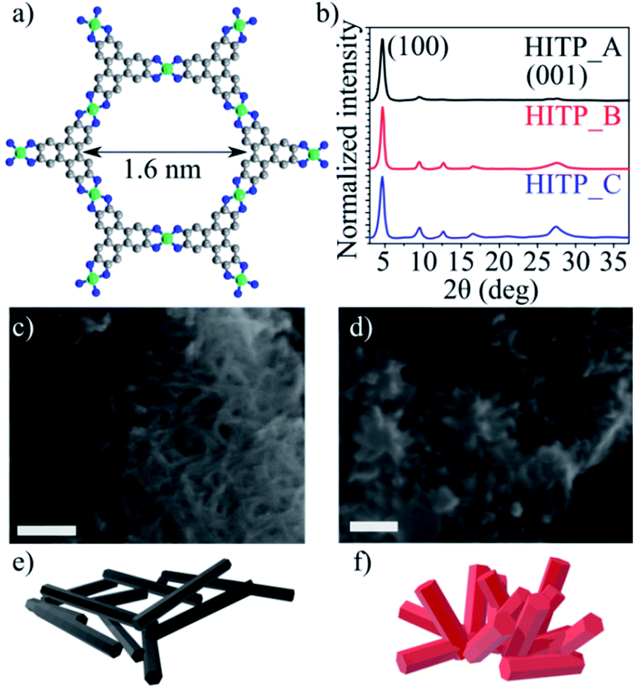 | ||
| Fig. 1 Ni3(HITP)2 molecular structure as a ball-and-stick model, where carbon is grey, nickel is green and nitrogen is blue (a), normalized intensity PXRD patterns of the three Ni3(HITP)2 batches (b), SEM micrographs of HITP_A (c) and HITP_B (d), where the scale bar is 200 nm, 3D schematics of the crystal morphology for HITP_A (e) and HITP_B (f) based on the arrangement seen in the SEM images; HITP_C shows the same morphology as HITP_B (Fig. S1†). | ||
Another notable difference is the aggregation behavior of the crystallites in the three samples. HITP_A presents as bulky agglomerates with diameters ranging from 500 nm to over 2 μm, with intertwined individual crystallites, forming a texture akin to planar intertwined wire segments (Fig. 1e). For both HITP_B and HITP_C, the agglomerates are smaller, on the order of 200–500 nm, and they are more hierarchical, with small crystals branching out of the plane of the agglomerates (Fig. 1f). These differences in morphology may explain why the longer crystallites exhibit a smaller nitrogen-accessible BET surface area then the shorter ones. The hierarchical, branched out morphology is beneficial for penetration of the pores by the gas molecules, whereas the intertwined morphology, in which the only available entrances to the internal pores are at the end faces of the crystallites and the majority of pore entrances are obscured by other crystallites, can yield lower apparent BET surface areas.
In the electrochemical testing of electrodes made from each of the MOF samples, the CV shapes do not show any pronounced redox events (Fig. 2a and b). The retention curves show that for rates lower than 2 mV s−1, the capacitance values saturate. This may be related to fully filling the pores with the electrolyte ions for electrostatic charge storage (Fig. 2c). The 1 mV s−1 values can therefore be regarded as ‘saturation’ values of the capacitance that should not increase substantially when cycling at lower speeds. They can also be regarded as the capacitance values best related to the microstructure and physical properties of the material itself. The measured capacitances reach 21.9, 100.8 and 74.5 F g−1 for HITP_A, HITP_B, and HITP_C, respectively, which when normalized to the BET surface areas equate to 8.4, 12.2 and 12.7 μF cm−2 (see Table 2). Once again, the value for HITP_A diverges significantly from the values for the two other batches, in line with the observations derived from the morphology and PXRD.
 | ||
| Fig. 2 Results of characterization of 3 electrode cells prepared from the three different Ni3(HITP)2 batches. Cyclic voltammetry at 1 mV s−1 (a) and 100 mV s−1 (b). Capacitance retention as a function of the voltage sweep rate (c). Electrochemical impedance spectra (d). | ||
| Sample | Capacitance (F g−1) | Capacitance (μF cm−2) | ESR (Ω) | R CT (Ω) | EDR (Ω) |
|---|---|---|---|---|---|
| HITP_A | 21.9 | 8.4 | 1.6 | 68 | 69 |
| HITP_B | 100.8 | 12.2 | 1.6 | 9.9 | 15 |
| HITP_C | 74.5 | 12.7 | 0.6 | 10.4 | 14 |
The difference in the observed normalized capacitance can be explained by the very large total internal resistance of the electrode made from HITP_A.
A closer look at the CV shapes reveals that the smallest area CV scan (HITP_A) also displays the largest curvature of the current characteristic after the voltage direction switch. For an ideal electrostatic double layer capacitor, the CV plot is a rectangle with immediate current switching following the change in the direction of the voltage sweep. For a real device, the total internal resistance of the device plays a dominant role, slowing down the current switching speed, resulting in a CV trace with rounded corners, which translates to less surface area within the CV trace than there would be for an ideal capacitor. This total internal resistance, RTI, is related to both the electronic electrode resistance and the ionic electrolyte resistance (represented jointly by the equivalent series resistance, ESR) and the resistance related to filling and emptying of the pores during charging and discharging (called the equivalent distributed resistance, EDR).
To determine the ESR and EDR, we recorded electrochemical impedance spectra for all the samples, and all display a qualitatively similar shape, a depressed high frequency semicircle to which an inclined straight line is attached for lower frequencies (Fig. 2d). The ESR values, extracted from the high frequency region of the EIS, are 1.6 Ω for both HITP_A and HITP_B, and 0.6 Ω for HITP_C. The radii of the depressed semicircles evidence the most visible differences between the samples, again showing poorer performance and higher impedance for the HITP_A cell in comparison with the other two. These radii are related to the so-called charge-transfer resistance, RCT, which for EDLC cells can be related to the rate of depolarization of the electrolyte ions inside the electrode upon changing the applied electrical field. The last part of the EIS, the inclined line, is related to the diffusion of ions in the area adjacent to the electrode. The total internal resistance was extracted from the intercept of the interpolation of the low frequency data of the inclined line with the real axis and was used to determine the EDR (see Table 2).
The electrochemical response of the electrodes can be explained based on the material morphology. Because the Ni3(HITP)2 crystals preferentially grow along the c-axis,10 the long, needle-like material has crystallites displaying small facets in the ab plane (needle ends), and large facets in the ac or bc crystallographic planes. On the other hand, the shorter crystals expose larger facets in the ab plane and smaller facets in planes containing the c axis. On the atomic scale, the facets normal to the crystallographic c axis are those that allow access to the 1.6 nm-wide channels, whereas the facets parallel to the c axis have no obvious openings, all displaying closely stacked monolayers of Ni3(HITP)2 that are impermeable to hydrated K+ ions from the electrolyte. The latter is also confirmed by the absence of intercalation peaks in the CV. Taking into account also the general morphology of the powder, with the intertwined, agglomerated structures in HITP_A and the branched out structures in HITP_B and HITP_C, we can surmise that the branched out materials display larger capacitances due to the larger area available for solvated ions to penetrate the pores, in contrast to the longer crystallites where ion penetration is limited.
These observations are borne out by the CV retention data: high voltage sweep rates limit pore penetration, and the CV response is primarily related to the external surface of the crystalline agglomerates and is much lower for HITP_A than for the other batches. The charge transfer resistance also follows the aspect ratio of the crystals available for insertion. The HITP_A![[thin space (1/6-em)]](https://www.rsc.org/images/entities/char_2009.gif) :HITP_B EDR ratio is 4.6, while the HITP_A:HITP_C EDR ratio is 4.9. Both correlate with the actual aspect ratio differences between HITP_A and HITP_B, 3.6, and between HITP_A and HITP_C, 4.5 (see Table 1). The charge transfer resistances are related to the longer crystallites, since it takes a longer time for ions to penetrate the longer slits than the shorter ones.
:HITP_B EDR ratio is 4.6, while the HITP_A:HITP_C EDR ratio is 4.9. Both correlate with the actual aspect ratio differences between HITP_A and HITP_B, 3.6, and between HITP_A and HITP_C, 4.5 (see Table 1). The charge transfer resistances are related to the longer crystallites, since it takes a longer time for ions to penetrate the longer slits than the shorter ones.
Comparing different batches allows us to distinguish the two most significant contributions to the capacitance of a given 2D MOF. Surprisingly, we find that both are related to morphology rather than any intrinsic parameter. The first is related to the shape of the individual crystals, and the second to the agglomerates comprising the batch. The latter significantly affects the observed gravimetric surface area of the material, even though it likely does not indicate differences in intrinsic porosity. Surprisingly, the changes in conductivity over 2 orders of magnitude did not correlate significantly with the observed capacitance. Clearly, the lower the conductivity, the higher the ESR of the electrodes, but the EDR also plays a role in real life devices and is not directly related to the conductivity itself.
Conclusions
Although quantifying the electronic or intrinsic contributions of the material itself, here Ni3(HITP)2, would likely require considerable computational resources and lies outside the scope of our report, the foregoing results allow us to compile a set of general rules which make possible the in-lab optimization of a 2D MOF material or other similarly anisotropic porous materials for electrolytes based on observable quantities such as crystal length, aspect ratio, and agglomeration behavior (e.g. branched-out, intertwined, etc.):(1) A determining factor for the electrochemical behavior of a given 2D MOF is the apparent surface area, which is clearly correlated with the mesostructural morphology. In this sense, a branched out, hierarchical structure is preferred to a globular one;
(2) The longer the individual crystals, the larger the EDR of the electrode, limiting both the observable capacitance and the power available from the full device. The EDR cannot be determined based on the bulk conductivity of the MOF;
(3) Differences in electrical conductivity between batches of up to two orders of magnitude seem inconsequential for capacitance. Importantly, we note that for good electrical polarization, materials should exhibit electrical conductivity of at least ∼10−4 S cm−1.
Finally, we note that the first two points likely do not hold for materials that present three-dimensional pores. For such materials, although agglomeration of crystallites is still likely to impede ion penetration, the effects may be less pronounced.
Conflicts of interest
There are no conflicts to declare.Acknowledgements
This research was funded by Automobili Lamborghini S. P. A. I. S. thanks the Research Foundation Flanders (FWO) for a postdoctoral fellowship. Part of the characterization was performed at the Center for Nanoscale Systems (CNS), a member of the National Nanotechnology Infrastructure Network (NNIN), which is supported by the National Science Foundation under NSF award no. ECS-0335765. CNS is part of Harvard University.Notes and references
- L. S. Xie, G. Skorupskii and M. Dincă, Chem. Rev., 2020, 120, 8536–8580 CrossRef CAS PubMed.
- E. M. Miner, T. Fukushima, D. Sheberla, L. Sun, Y. Surendranath and M. Dincă, Nat. Commun., 2016, 7, 10942 CrossRef CAS PubMed.
- I. Stassen, N. Burtch, A. Talin, P. Falcaro, M. Allendorf and R. Ameloot, Chem. Soc. Rev., 2017, 46, 3185–3241 RSC.
- W. P. Lustig, S. Mukherjee, N. D. Rudd, A. V. Desai, J. Li and S. K. Ghosh, Chem. Soc. Rev., 2017, 46, 3242–3285 RSC.
- K. J. Erickson, F. Léonard, V. Stavila, M. E. Foster, C. D. Spataru, R. E. Jones, B. M. Foley, P. E. Hopkins, M. D. Allendorf and A. A. Talin, Adv. Mater., 2015, 27, 3453–3459 CrossRef CAS PubMed.
- K. AlKaabi, C. R. Wade and M. Dincă, Chem, 2016, 1, 264–272 CAS.
- D. Feng, T. Lei, M. R. Lukatskaya, J. Park, Z. Huang, M. Lee, L. Shaw, S. Chen, A. A. Yakovenko, A. Kulkarni, J. Xiao, K. Fredrickson, J. B. Tok, X. Zou, Y. Cui and Z. Bao, Nat. Energy, 2018, 3, 30–36 CrossRef CAS.
- D. Sheberla, J. C. Bachman, J. S. Elias, C.-J. Sun, Y. Shao-Horn and M. Dincă, Nat. Mater., 2017, 16, 220–224 CrossRef CAS PubMed.
- D. Sheberla, L. Sun, M. A. Blood-Forsythe, S. Er, C. R. Wade, C. K. Brozek, A. Aspuru-Guzik and M. Dincă, J. Am. Chem. Soc., 2014, 136, 8859–8862 CrossRef CAS PubMed.
- R. W. Day, D. K. Bediako, M. Rezaee, L. R. Parent, G. Skorupskii, M. Q. Arguilla, C. H. Hendon, I. Stassen, N. C. Gianneschi, P. Kim and M. Dincă, ACS Cent. Sci., 2019, 5, 1959–1964 CrossRef CAS PubMed.
Footnotes |
| † Electronic supplementary information (ESI) available: Materials and experimental data, additional SEM images of the material from three batches as well as the N2 adsorption isotherms and BET fits for all batches. See DOI: 10.1039/d1fd00028d |
| ‡ Currently at Łukasiewicz Research Network – Institute of Microelectronics and Photonics, Warsaw, Poland. |
| § Currently at ASM Pacific Technology Ltd., Billerica, MA, USA. |
| This journal is © The Royal Society of Chemistry 2021 |