
Insights into interface and bulk defects in a high efficiency kesterite-based device†
Robert
Fonoll-Rubio
a,
Jacob
Andrade-Arvizu
 a,
Javier
Blanco-Portals
bc,
Ignacio
Becerril-Romero
a,
Maxim
Guc
*a,
Edgardo
Saucedo
ad,
Francesca
Peiró
bc,
Lorenzo
Calvo-Barrio
ef,
Maurizio
Ritzer
g,
Claudia S.
Schnohr
gh,
Marcel
Placidi
ad,
Sònia
Estradé
bc,
Victor
Izquierdo-Roca
*a and
Alejandro
Pérez-Rodríguez
af
a,
Javier
Blanco-Portals
bc,
Ignacio
Becerril-Romero
a,
Maxim
Guc
*a,
Edgardo
Saucedo
ad,
Francesca
Peiró
bc,
Lorenzo
Calvo-Barrio
ef,
Maurizio
Ritzer
g,
Claudia S.
Schnohr
gh,
Marcel
Placidi
ad,
Sònia
Estradé
bc,
Victor
Izquierdo-Roca
*a and
Alejandro
Pérez-Rodríguez
af
aCatalonia Institute for Energy Research – IREC, Sant Adrià de Besòs, 08930, Barcelona, Spain. E-mail: vizquierdo@irec.cat; mguc@irec.cat
bLENS-MIND, Departament d'Enginyeria Electrònica i Biomèdica, Universitat de Barcelona, 08028, Barcelona, Spain
cInstitute of Nanoscience and Nanotechnology (IN2UB), Universitat de Barcelona, 08028, Barcelona, Spain
dPhotovoltaic Group, Electronic Engineering Department, Universitat Polytècnica de Catalunya (UPC), 08034, Barcelona, Spain
eCentres Científics i Tecnològics (CCiTUB), Universitat de Barcelona, C/Lluis Solé i Sabaris, 08028 Barcelona, Spain
fDepartament d'Enginyeria Electrònica i Biomèdica, INUB, Universitat de Barcelona, C/Martí i Franqués 1, 08028 Barcelona, Spain
gInstitut für Festkörperphysik, Friedrich-Schiller-Universität Jena, Max-Wien-Platz 1, 07743 Jena, Germany
hFelix-Bloch-Institut für Festkörperphysik, Universität Leipzig, Linnéstraße 5, 04103 Leipzig, Germany
First published on 24th December 2020
Abstract
This work provides a detailed analysis of a high efficiency Cu2ZnSnSe4 device using a combination of advanced electron microscopy and spectroscopy techniques. In particular, a full picture of the different defects present at the interfaces of the device and in the bulk of the absorber is achieved through the combination of high resolution electron microscopy techniques with Raman, X-ray fluorescence and Auger spectroscopy measurements at the macro, micro and nano scales. The simultaneous investigation of the bulk and the interfaces allows assessing the impact of the defects found in each part of the device on its performance. Despite a good crystalline quality and homogeneous composition in the bulk, this work reports, for the first time, direct evidence of twinning defects in the bulk, of micro and nano-voids at the back interface and of grain-to-grain non-uniformities and dislocation defects at the front interface. These, together with other issues observed such as strong absorber thickness variations and a bilayer structure with small grains at the bottom, are shown to be the main factors limiting the performance of CZTSe devices. These results open the way to the identification of new solutions to further developing the kesterite technology and pushing it towards higher performances. Moreover, this study provides an example of how the advanced characterization of emergent multilayer-based devices can be employed to elucidate their main limitations.
Broader contextCurrent cutting-edge environmentally-friendly energy generation devices usually present multi-component and multi-layer complex structures. One example of this type of devices are the new earth abundant generations of chalcogenide-based thin film solar cell concepts like kesterites. Although this technology has already shown a high potential for the fabrication of sustainable solar cell devices, it still suffers from the several limitations that strongly impact device performance and do not allow reaching the commercial state. The complex nature of these devices makes necessary an advanced characterization of the main properties at the macro-, micro- and nano scales for a deep understanding of these limitations. This work represents a reliable demonstration of a combinatorial analysis for compositional and structural study of kesterite solar cells that provides a full picture of the main factors limiting their performance including compositional inhomogeneities, structural defects, and degradation in the interfaces. As such, the results presented in this work open the way to the identification of new solutions that will aid to further develop the kesterite technology and push it towards higher performances contributing in the clean, responsible, and sustainable energy production necessary for a greener future. |
Introduction
Thin film photovoltaic (PV) technologies based on CdTe and Cu(In,Ga)Se2 (CIGS), have reached an advanced degree of maturity with proven efficiencies at the laboratory scale beyond 22%.1,2 These efficiency values combined with the inherent advantages of thin film PV such as low material usage, fabrication versatility or their easy integration (e.g. building integrated photovoltaics, wearables, internet of things, etc.) open the way to the democratization and ubiquity of PV through mass production of cheap and efficient solar cell devices. However, the dependence of these technologies on scarce elements like Te, In and Ga inevitably sets a limit to their future production yield restraining their mass deployment below the TW/year scale.3–5 In this context, Cu2ZnSn(SxSe1−x)4 (CZTSSe) and related compounds, also known as kesterites, represent a promising Earth-abundant alternative for thin film PV with higher potential for a future low cost mass production of PV devices. However, despite the great similarities in composition and crystal structure of CZTSSe and CIGS, the best efficiency achieved for a kesterite-based device at laboratory scale has been stagnated at 12.6% for more than 6 years.6,7 In the case of pure selenide kesterites (CZTSe), on which this work is focused, the best device reported so far exhibits a slightly lower efficiency, just below 12%.8In order to understand the origin of such a large performance gap between CIGS and CZTSSe, it is useful to take a look at the characteristics of comparable devices fabricated with both technologies. The first four rows of Table 1 show the main optoelectronic parameters of the two highest efficiency CuInSe2 (CISe) and CZTSe devices reported in the literature.8–11 Taking a look at the record CZTSe device,8 it can be observed that the main differences with CISe are found in the short-circuit current (Jsc) and open-circuit voltage (Voc) while the fill factor (FF) is similar for both technologies. However, the differences in the Jsc cannot be considered critical since this parameter can be greatly enhanced by optimizing the optical configuration of the solar cell for better light collection (e.g. texturing, choice of window layers, anti-reflective coatings, etc.) as in the case of the second best CZTSe device11 which shows a Jsc value similar to that of CISe. This is not the case for the Voc, which is more intimately related to the intrinsic limitations of the technology. These limitations can be clearly observed by looking at the Voc deficit (defined as Eg/q − Voc) values reported in Table 1. Compared to the highest efficiency CISe device,9 the Voc deficit of the CZTSe devices is around 250 mV higher. Nevertheless, this comparison is not entirely fair since this CISe device was fabricated with a Ga-enriched back interface and a RbF post-deposition treatment at the front interface. A more adequate comparison can be made with the second best CISe device which does not include these additional features.10 The Voc deficit of the CZTSe devices, in this case, is still around 130 mV higher. As such, it is evident that the main limitations of the CZTSe technology arise from this parameter. The origin of such a high Voc deficit in kesterites has been attributed to several issues taking place at different parts of the device. To mention some:
| Technology | V oc (mV) | J sc (mA cm−2) | FF (%) | Efficiency (%) | E g (eV) | E g/q − Voc (mV) | Ref. |
|---|---|---|---|---|---|---|---|
| a With a Ga-enriched back interface and a RbF post-deposition treatment at the front interface. | |||||||
| CISea | 609 | 42.3 | 74.6 | 19.2 | 1.00 | 391 | 9 |
| CISe | 491 | 40.6 | 75.2 | 15.0 | 1.00 | 509 | 10 |
| CZTSe | 432 | 36.3 | 76.2 | 11.9 | 1.07 | 638 | 8 |
| CZTSe | 423 | 41.7 | 66.6 | 11.7 | 1.07 | 647 | 11 |
| CZTSe | 434 | 33.8 (36.8) | 63.0 | 9.2 (10.0) | 1.04 | 606 | This work |
I. At the front interface: non-optimum band alignment with the CdS buffer layer,12–15 Fermi level pinning due to CuZn antisite point defects,16 incomplete CdS coverage,17,18 high density of interface defects,19,20 as well as ZnSe21 and SeO2/Sn(O,Se)x22 secondary phase formation.
II. In the bulk: Cu–Zn disordering leading to bandgap and electrostatic potential fluctuations,23–29 formation of secondary phases that can lead to compositional fluctuations and induce the formation of defects,21,30–32 non-passivated grain boundaries33 and short minority carrier lifetime.27,34
III. At the back interface: defective coupling with the back contact and chemical instability12,13,35–37 as well as an excessive MoSe2 formation that may alter the back band alignment unfavorably.38
Possible solutions of the listed above problems were proposed by several authors. For instance, the use Cu-poor Zn-rich compositions allows minimizing the formation of CuZn antisite point defects at the front interface.23 Although these compositional regime may lead to a more likely formation of ZnSe, selective etchings have been proposed to effectively remove this and other secondary phases from the surface of the kesterite absorber after synthesis.21,30 Front interface recombination can also be reduced through surface passivation treatments11,39 or the use of passivating nanolayers.17,20,40,41 Regarding the back interface, the use of a thin ZnO layer on the Mo back contact has been demonstrated to reduce chemical instability36 and the thickness of the MoSe2 layer can be controlled through multilayer Mo configurations and the use of selenization barriers.37 Finally, in the bulk of the absorber, partial substitution of Cu by Ag or of Zn by Cd has been proposed to reduce Cu–Zn disordering15,16 and Na-doping is commonly regarded as a means of grain boundary passivation.42
Nevertheless, most of the studies of kesterite-based devices typically focus on only one part of the device, i.e. in the bulk or in one of the interfaces, while the most likely explanation for the high Voc deficit of kesterites is a combination of several issues taking place simultaneously in different parts of the device.43,44 In this context, this work aims at providing a complete analysis of a high efficiency CZTSe device using a combination of advanced microscopy and spectroscopy techniques. In particular, the combination of high resolution electron microscopy techniques with Raman, X-ray fluorescence and Auger spectroscopy measurements at the macro, micro and nano scales allows us building a full picture of the different defects present at the front and back interfaces as well as in the bulk of the absorber and of how they affect the optoelectronic characteristics of the device with a focus on the Voc. We are able to show, for the first time, direct proof of the formation of twinning defects in the bulk of the absorber, nano and micro-voids at the back interface as well as grain-to-grain non-uniformity and point and line defects at the front interface within the same high efficiency CZTSe device. The observations made and the results obtained in this work represent an important insight in the complete understanding of the main limitations of CZTSe based devices. Moreover, the present work represents an example of an advanced characterization study of a complex system (thin film solar cell) that may serve as an instructive handbook to help building up the full picture of multilayer-based devices for a broad spectrum of readers and researchers.
Results
Optoelectronic characterization
Using the preparation process described in the Experimental section, a sample with 20 individual solar cells (3 × 3 mm2) was fabricated (Fig. 1c). The illuminated and dark J–V curves as well as the main optoelectronic parameters of the best solar cell obtained in the sample are shown in Fig. 1a. In addition, Fig. 1b shows the external quantum efficiency (EQE), internal quantum efficiency (IQE), and reflectance of the record device. A 9.2% record efficiency device with a 1.04 eV bandgap (calculated from the EQE using the derivative method, see bottom of Fig. 1b) was achieved. Both the Voc (434 mV) and Voc deficit (606 mV) of this device are very close to those reported for the best CZTSe devices shown in Table 1. However, the difference between the EQE and IQE curves indicates that the device presents important reflectance losses, especially in the 500–750 nm region. By correcting these reflectance losses, the gain in Jsc (value in brackets in Table 1 and Fig. 1a) could potentially increase the efficiency of this device up to 10%. In addition, the device was fabricated following the procedure employed for our in-house champion CZTSe solar cell (11.0%)45 but without an optimized structure (i.e. without anti-reflecting coating, metallic grid, etc.). Thus, it is safe to assume that the device studied in this work can be considered inside the state-of-the-art and that the limitations of the Voc identified throughout this work are universal and, thus, relevant for other high efficiency CZTSe devices. On the other hand, the slightly lower efficiency of the device fabricated in this work can be attributed to its lower Jsc and FF. Regarding the former, besides reflectance losses, the main limitation of the Jsc seems to arise from a low collection at the near infrared (NIR) of long wavelength (>750 nm) photons. This could be indicating that the device suffers from either light absorption issues, recombination issues or a combination of both. As for the low FF, it can be directly linked to the high series resistance (Rs) found in the device (2–5 times higher than previously reported values).8,11 However, if long wavelength collection is limited by recombination issues, these would further contribute in lowering the FF of the device. All these issues together with the possible limitations of the Voc of CZTSe solar cells will be explored throughout the upcoming analysis.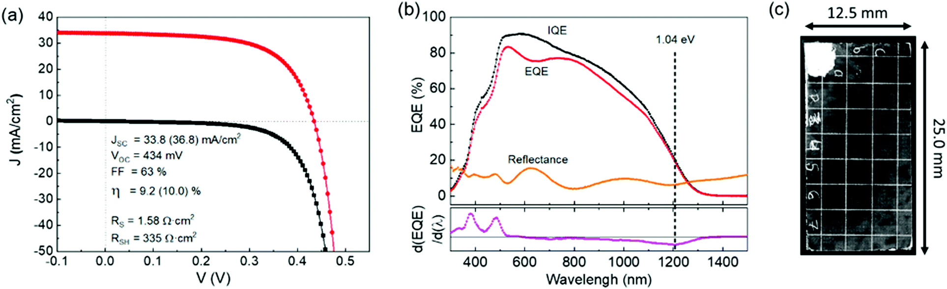 | ||
| Fig. 1 (a) Illuminated (red) and dark (black) J–V curves together with the main optoelectronic parameters of the best CZTSe solar cell fabricated in this work. The values in brackets were calculated by correcting the reflection losses. (b) EQE, IQE and reflectance curves of the same device. The bottom part shows the first derivative of the EQE curve employed to estimate the bandgap of the absorber. (c) Optical image of the CZTSe sample with the individual 3 × 3 mm2 solar cells. | ||
Bulk characterization
The overall morphology of the 9.2% CZTSe device fabricated in this work was studied by means of scanning electron microscopy (SEM) and scanning transmission electron microscopy (STEM) in cross section configuration. Fig. 2 shows a collage of a series of cross-sectional SEM and bright field (BF) STEM images of the full device where the different layers (including the Pt layer added during focused ion beam (FIB) sample preparation) are indicated. The comparison between both techniques allows discarding the presence of artefacts in the STEM image generated during lamella preparation. An irregular CZTSe absorber morphology with thickness variations in the 0.9–1.3 μm range is detected, which generates undulating buffer and window layers and, thus, a rough surface. Besides surface roughness, the varying absorber thickness also influences the thickness of the upper layers (In2O3–SnO2 (ITO) thickness – 100 to 170 nm, i-ZnO thickness – 40 to 130 nm, and CdS thickness – 40 to 90 nm). Another interesting feature that can be spotted in Fig. 2 is the presence of very bright areas that indicate the existence of multiple voids at the back interface. These can also be observed as dark areas in the dark field (DF) image presented in Fig. S1 (ESI†). The origin of these voids and their possible effects on device performance will be studied in more detail later on.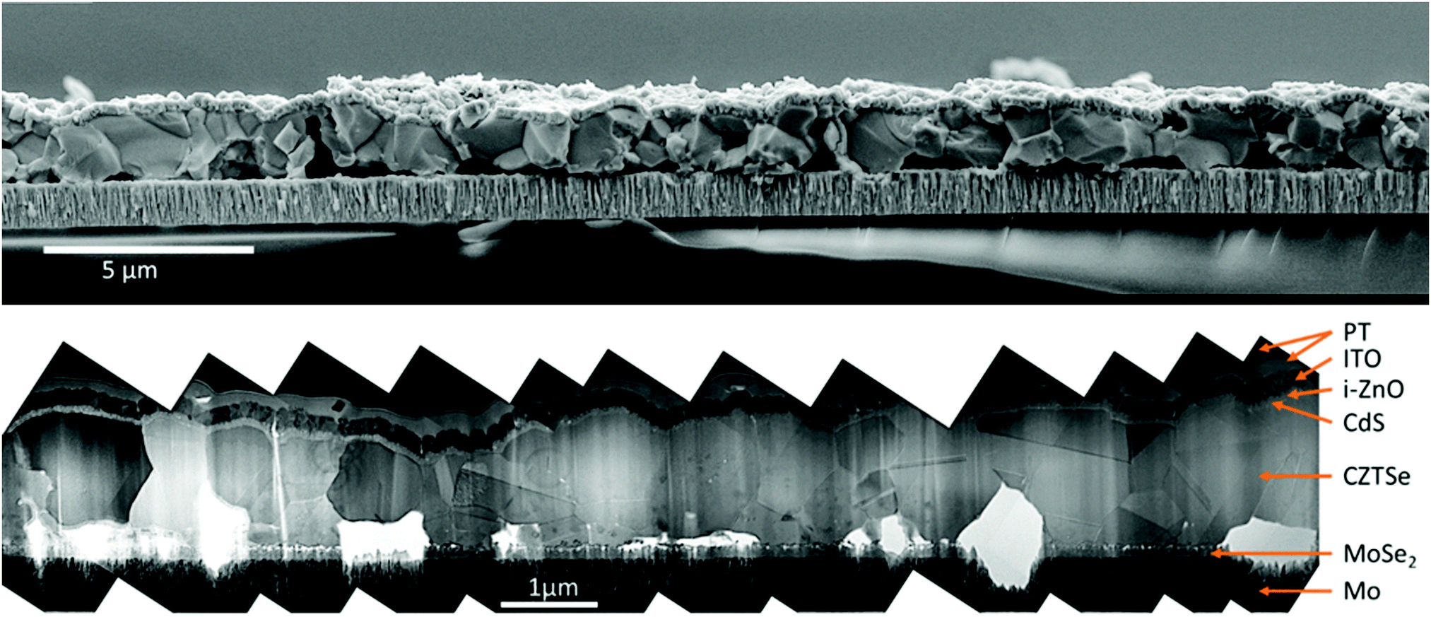 | ||
| Fig. 2 Collage image of a series of cross-sectional SEM (top) and STEM (bottom) images of a CZTSe-based solar cell in bright field configurations. The different observed layers of the device are indicated in the STEM image, including the platinum layer added during FIB sample preparation. | ||
Besides the void-related bright areas, subtler contrast differences can be also detected in Fig. 2 within the CZTSe absorber layer. These can be attributed to two main different effects. First, the different crystalline orientation of the different grains of the absorber results in different contrasts in the image. This contrast difference enables to study the grain boundaries present in the CZTSe absorber in detail. Several columnar grains that extend throughout the whole thickness of the absorber and are formed by vertical grain boundaries with the regular shape can be observed both in SEM and STEM images (Fig. 2). However, a closer look reveals that there exist specific absorber regions with a bilayer structure (Fig. 3a) in which large micron-sized grains (1–2 μm2) occupy the top part of the absorber layer, and smaller submicron grains (∼0.3 μm2) form the bottom part. This can be better observed in Fig. 3a.2 where the grain boundaries are highlighted in red. In order to study the possible distortion of the CZTSe crystal structure around the grain boundaries, a high-resolution high angle annular dark field (HAADF) image of a grain boundary was acquired (Fig. 3b). Fast Fourier transformations (FFTs) were made on the HAADF image at a region completely inside a grain and at a region extending from the grain boundary limit to 5 nm inside the grain (Fig. 3b). The similarity between both FFTs indicates that the grain boundary does not distort the crystal structure noticeably.
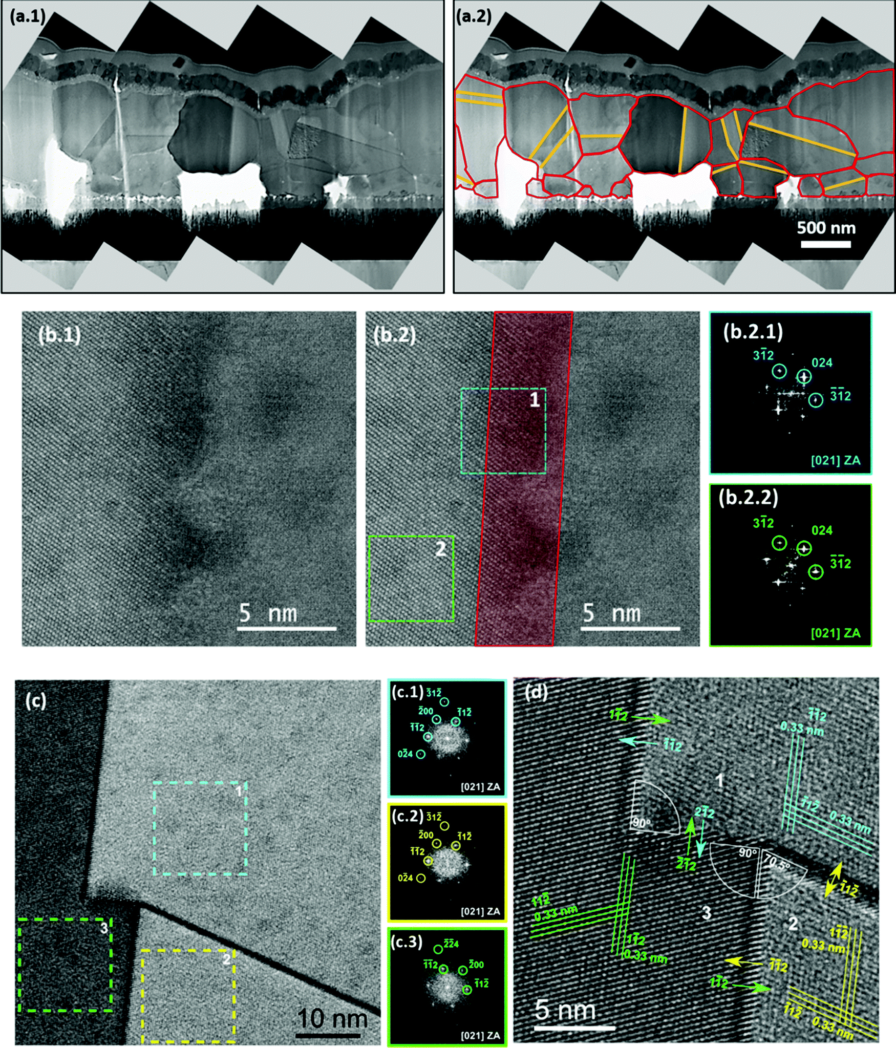 | ||
| Fig. 3 (a) Cross-sectional STEM images of a CZTSe-based solar cell in bright field configuration with indication of different grains (red lines) and twinning (orange lines) in the right image. (b) Cross-sectional HAADF of two different grains and their grain boundary with (b.2.1.–b.2.2) FFTs of corresponding regions indicated by the dashed rectangles. The region in red, indicates the grain boundary. (c) Cross-sectional HRTEM image of the bulk of the CZTSe absorber at a region with twinning defects and (c.1–c.3) FFT of the corresponding regions indicated by dashed rectangles. (d) Magnified spotty patterns of the HRTEM image of the triple junction area shown in in (c). Visual guidelines are included for some of the families of atomic planes resolved in the FFTs. The directions of the families of planes forming the twinning defects and angles between them are also included. | ||
The second effect influencing the contrast in the STEM images, is related to twinning defects inside the grains (highlighted in orange in Fig. 3a.2). These were studied in detail through high-resolution transmission electron microscopy (HRTEM) images and are presented in Fig. 3c. Although at first glance, the HRTEM image seems to correspond to a triple grain boundary, a careful analysis of the atomic planes and the boundaries shows that it is a twinning defective region. FFT analyses were made on the three regions tagged as dashed squares in Fig. 3c and labelled as 1, 2 and 3. The patterns obtained indicate that the three regions analysed are oriented very close to the [021] zone axis (ZA). However, by further magnifying the spotty patterns of the HRTEM image (Fig. 3d), it can be observed that while the crystalline planes are well resolved for region 3, a slightly worse resolution and contrast of the atomic planes is detected in regions 1 and 2. This points out that regions 1 and 2 are slightly deviated from the [021] ZA. Furthermore, the angles of the crystalline planes shown in Fig. 3d indicate that region 3 is rotated with respect to regions 1 and 2 around the axis of observation. This is a usual feature of twinning defects. Nonetheless, the clear and defined spotty patterns indicate that, despite twinning, the grains in the bulk region of the absorber display a good crystalline quality. Although evidences of the formation of twin boundaries in CZTSe have been recently reported,46 to the best of our knowledge, this is the first time that twinning defects are directly observed for this material.
A more detailed analysis of the crystal structure inside a grain of the bulk of the CZTSe absorber was made through a HAADF image and is shown in Fig. 4. The image on the left is a denoised version of the original image, and was obtained by applying a mask to the FFT (red inset in Fig. 4, left) and then carrying out an inverse-FFT (iFFT). The original image can be consulted in Fig. S2 (ESI†). The zoomed region highlighted in green shows that the lateral resolution enables the identification of the dumbbell structure (Fig. 4, right-top). The structure observed is in good agreement with the proposed atomic model for the kesterite type structure (space group I![[4 with combining macron]](https://www.rsc.org/images/entities/char_0034_0304.gif) and space number 82),47 when observed from the [021] ZA (see Fig. 4, right top and bottom). The slight differences that may be observed in the image with respect to the kesterite structure may arise from tiny tilting deviations from the exact [021] ZA during the observation. Finally, some interplanar distances were measured in Fig. 4 and the results obtained are in good agreement with the crystalline structure of kesterite CZTSe (PDF #04-010-6295).
and space number 82),47 when observed from the [021] ZA (see Fig. 4, right top and bottom). The slight differences that may be observed in the image with respect to the kesterite structure may arise from tiny tilting deviations from the exact [021] ZA during the observation. Finally, some interplanar distances were measured in Fig. 4 and the results obtained are in good agreement with the crystalline structure of kesterite CZTSe (PDF #04-010-6295).
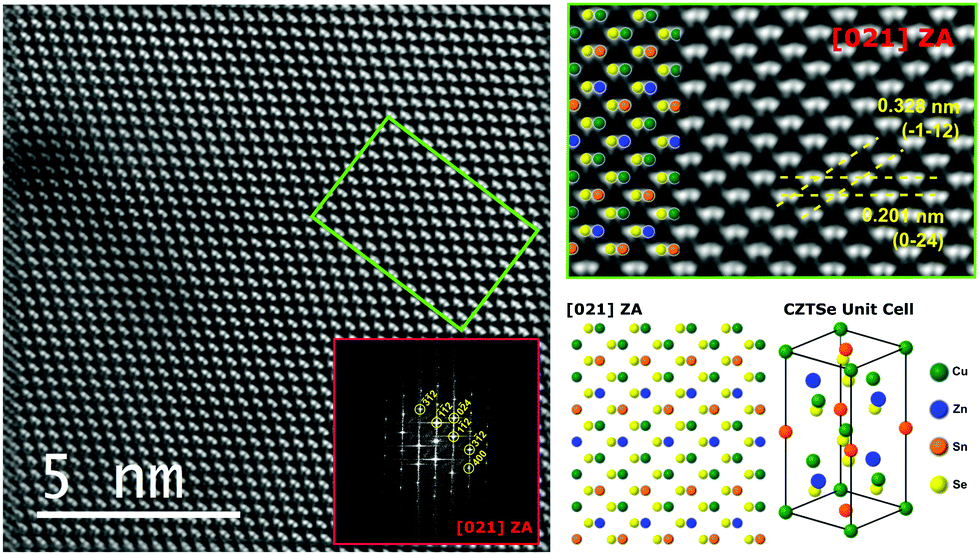 | ||
| Fig. 4 On the left, iFFT of a HAADF filtered image of a CZTSe grain. Red inset: FFT of the whole area of the image. The area in green is zoomed on the right, where an overlay of the atomic structure and the HAADF image is shown at the top with some of the atomic planes resolved in yellow. In the right-bottom image, the atomic structure of the kesterite in [021] ZA is displayed. | ||
In order to complete the study of the bulk of the CZTSe absorber, its chemical composition was analysed by means of a nano-X-ray fluorescence (XRF) mapping performed on a thin cross-section lamella sample (see Fig. 5). The composition of each measuring point was averaged over the whole thickness of the lamella (260 nm) and the region analysed included at least 6 different grains. Despite the strong thickness variation and the presence of relatively large voids at the back interface, the cation ratio deviation maps (Fig. 5d) show a quite homogeneous composition with no noticeable intra-grain or inter-grain differences or variations at the grain boundaries. Note that despite the size of the beam spot of roughly 50 nm, nanoXRF is well capable of resolving compositional variations of nanosized features like grain boundaries as demonstrated for both CZTSe46 and CIGS.48 In order to go in depth into the homogeneity analysis in the nanoXRF mappings, several scanning lines parallel and perpendicular to the absorber surface were selected. The parallel scanning lines show an overall homogeneous composition. Only in some specific points (e.g. at around 4 μm from the left side of the absorber) a decrease of the Zn content is observed. However, the perpendicular scanning lines (in-depth analysis) show a slight increase of the Cu content towards the back region of the absorber (see lines 2 and 3 in Fig. 5d, Δ([Cu]/([Zn] + [Sn])) from −0.04 to +0.04).
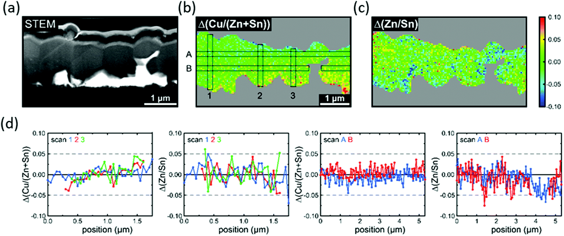 | ||
| Fig. 5 BF-STEM image (a) and mappings of the deviation of the [Cu]/([Zn] + [Sn]) (b) and [Zn]/[Sn] (c) cation ratios (calculated by subtracting the mean value obtained for the whole sample from the value obtained in each individual pixel). The grey regions (b) and (c) mark the areas where no absorber was present. The graphs at the bottom (d) show the cation ratio deviations (averaged over 3 pixels, 150 nm) along the vertical scans 1, 2, 3, and horizontal scans A, B, as indicated in the top middle panel. Scan B is interrupted in the region where the void is present. | ||
Back interface characterization
The CZTSe/back contact interface is characterized by small CZTSe grains (as discussed in the Bulk characterization section), a ∼100 nm MoSe2 layer (resulting from the partial selenization of the Mo back contact during annealing) and the presence of voids.The voids observed at the back interface of the CZTSe absorber in Fig. 2 and Fig. 5, were studied in more detail using cross-sectional STEM and planar view SEM images (Fig. 6). Two different types of voids can be distinguished in Fig. 6: large micrometric voids (orange rectangles) and small nanometric voids (red rectangles). The micrometric voids observed in cross-section SEM and STEM collage images can achieve sizes up to 0.5 μm2 (Fig. 2). This represents around 8% of the cross-section area of the CZTSe absorber layer and 37% of the contact interface length between CZTSe and Mo/MoSe2. A different perspective of the micrometric voids can be obtained from the planar view SEM image of the back interface of the absorber (obtained after mechanical lift-off) presented in Fig. 6b. This figure shows that the presence of large voids spreads over the whole back surface of the CZTSe absorber decreasing the contact area with the back contact. In particular, Fig. 6b shows that the contact area between CZTSe and Mo/MoSe2 back contact is around 40% of the total area of the image (in agreement with the cross-sectional analysis). In the case of the small nanometric voids, the cross-sectional STEM image shown in Fig. 6a allows estimating their size to a radius of some tens of nanometres. The presence of these small voids is also confirmed by the rough texture of the CZTSe grains observed in the planar SEM image of the back interface (Fig. 6b). These nanometric voids can create weak points that enable an easy and clean mechanical exfoliation process of the CZTSe absorber from the back contact layer.
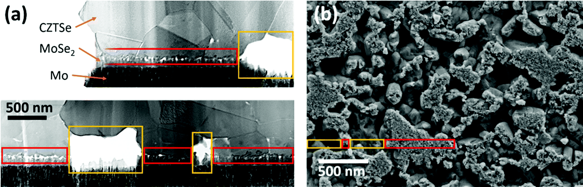 | ||
| Fig. 6 (a) Collage image of a series of cross-sectional STEM images of the CZTSe device. The CZTSe, MoSe2 and Mo layers in the back interface are indicated. (b) Planar view SEM image of the CZTSe back interface after being detached from the substrate by mechanical lift-off. Red squares indicate regions with nano-voids, and orange squares indicate micro-voids. | ||
In order to evaluate the CZTSe crystal quality, confirm the MoSe2 formation, and evaluate the possible formation of residual secondary phases at the back interface region, a detailed analysis of the Raman scattering spectra measured under 532 nm and 325 nm excitation wavelengths was performed on the back interface of the lifted-off CZTSe absorber, and on the substrate from which the absorber was detached. The use of 532 nm excitation wavelength enables the detection and analysis of the CZTSe phase together with possible formation of Cu–Sn–S and Sn–Se secondary phases.49 On the other hand, the 325 nm excitation wavelength shows a high sensitivity to the presence of the SnSe2 secondary phase which has been proven to be detrimental for the Voc of CZTSe devices.31 Likewise, the 325 nm excitation wavelength can also be used for analysing defect types and concentration in the CZTSe phase, which have strong impact on the optoelectronics properties of the device.49–52 The Raman spectra obtained under 532 and 325 nm excitation wavelengths are presented in Fig. 7a and b, respectively. Both spectra show mainly the CZTSe phase with some peaks of the MoSe2 phase on the back interface of the lifted-off absorber, while only MoSe2 peaks can be observed in the spectra obtained from the substrate. No additional peaks related to any secondary phases were observed in the spectra. The presence of MoSe2 peaks in the back side of the lifted-off absorber arises from the not perfect exfoliation process in which some MoSe2 remains attached to the absorber. These MoSe2 peaks are more intense under UV excitation due to its lower penetration depth (it does not typically exceed 10 nm in the case of CZTSe) which results in an analysed volume with a high proportion of MoSe2. This, in turn, results in a high overlapping of the CZTSe and MoSe2 peaks. In order to perform an analysis of the defects present in the CZTSe phase, the spectrum acquired from the substrate (pure MoSe2 phase) was mathematically subtracted from the spectrum acquired from the back side of the absorber for the 325 nm excitation wavelength. The different relative intensity of the MoSe2 peaks in the spectra acquired at back side of absorber and at the substrate indicates a different preferential structural orientation of MoSe2 on substrate and the absorber sides.53 Taking this into account, the Raman spectrum measured on the back side of the CZTSe absorber was corrected by recalculating the intensities in accordance to the texture53 (more details in Fig. S3 (ESI†)). The resulting spectrum was compared to a spectrum of a close-to-stoichiometric CZTSe absorber measured under the same excitation conditions (Fig. 7c). A clear variation in the peaks related to VCu and ZnSn were observed.50 These differences indicate that the CZTSe back region is Cu-poor (with higher concentration of the of the VCu point defect) and Zn-rich (with higher concentration of the ZnSn point defect).
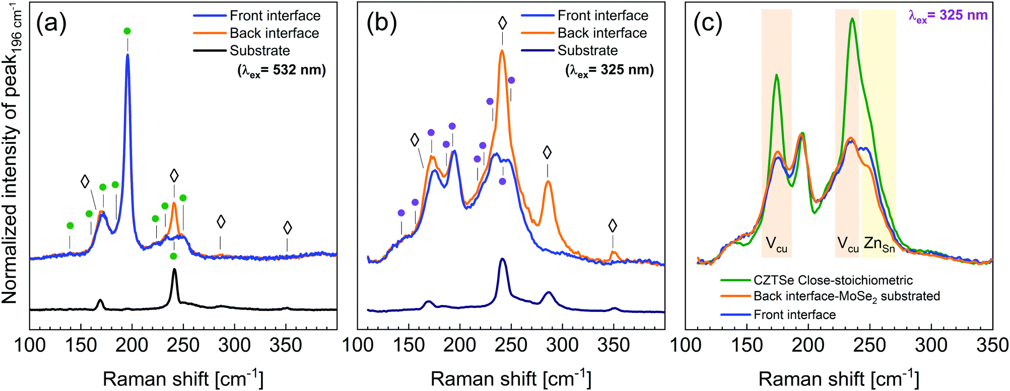 | ||
| Fig. 7 Raman spectra measured at CZTSe surface and back interface from CZTSe and MoSe2 sides under green (a) and UV (b) excitation wavelength. The dots (●) and diamonds (◊) indicates the position of the CZTSe47 and MoSe250 peaks, respectively. (c) Raman spectra of the close to stoichiometric CZTSe, measured on the absorber surface, and obtained from the back interface of the CZTSe after the MoSe2 subtraction. The shadow areas indicate the spectral regions related to VCu and ZnSn punctual defects in the CZTSe.47 | ||
Front interface characterization
The front interface of the record CZTSe device was analysed after chemically removing the CdS/i-ZnO/ITO top layer. Fig. 7a and b include the Raman spectra acquired at the front interface of the CZTSe absorber with 532 and 325 excitation wavelengths, respectively. Both spectra indicate that the main phase is the CZTSe kesterite type compound and no presence of the secondary phases can be detected. Similarly to the case of the back interface, the spectrum measured under UV excitation wavelength was employed to analyse defect formation in the CZTSe surface by comparing it to a reference stoichiometric CZTSe spectrum (Fig. 7c). The spectrum of the front interface shows a reduced relative intensity of the peaks at 175 and 250 cm−1 in comparison to the reference spectrum as in the case of the back interface. This is associated to the formation of the VCu and ZnSn point defects expected for the Cu-poor and Zn-rich composition of the absorber.50 However, a detailed comparison between the spectra of the CZTSe front and back interfaces reveals a different intensity of the VCu and ZnSn associated peaks. These differences are related to a slightly reduced VCu defect concentration and slightly increased ZnSn defect concentration at the CZTSe back interface region. These variations are in agreement with the small increase of the Cu content at the back interface observed by nanoXRF.In order to delve into the inhomogeneities in defect formation at the front interface of the absorber, that can have strong influence on the Jsc and Voc of the solar cell, a 20 × 20 μm2 micro-Raman mapping was performed (Fig. 8a). In the previous Raman measurements, a 70 μm spot was used and information was gathered from several grains in one measurement. Here, micro-Raman measurements, with a spot size <1 μm, allow analysing single grains of the absorber, thus providing information about phase and defect distribution along different grains. The micro-Raman mappings presented in Fig. 8a show a clear difference in the relative intensity of the peaks at 175 and 250 cm−1 measured under UV excitation wavelength. As mentioned above, the changes in the relative intensity of these peaks can be directly correlated to the changes in concentration of VCu and ZnSn point defects. The micro-Raman mappings were compared with AES compositional measurements carried out in a similar area of the absorber (Fig. 8b). The AES measurements show similar inhomogeneities in the [Cu]/([Zn] + [Sn]) and [Zn]/[Sn] cationic ratios between the different grains in agreement with the micro-Raman mappings while intragrain variations did not exceed the measurement error. AES is a highly sensitive technique for chemical composition measurements that provides information about the first 1–3 nm of the layer. Taking into account the relative penetration depth of the 325 nm laser used for the Raman analysis, the inhomogeneities detected in the distribution of defects can be directly associated to the compositional inhomogeneities detected by AES in line with reported results.49,50,54 On the other hand, both Raman and AES suggest a preferential composition in most grains analysed with just slightly different compositions in small regions of the grains. This is in agreement with the nanoXRF results, where only one of the six analysed grains showed small difference in the [Zn]/[Sn] ratio.
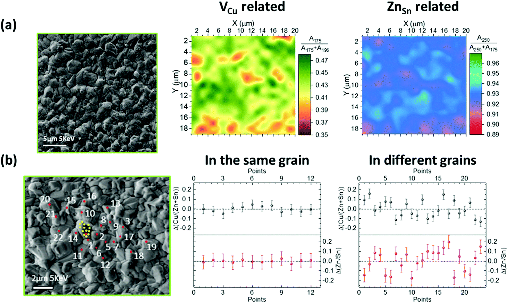 | ||
| Fig. 8 (a) Micro-Raman mappings of the defects distributions and (b) cations ratios estimated by AES in the CZTSe surface. SEM images of the absorber surface where micro-Raman and AES were carried out are presented on the left side. | ||
In order to exclude possible interlayer diffusion of elements, a compositional characterization of the interfaces between the window and buffer layers, and between the buffer and absorber layers was performed by EELS (Fig. 9). No interlayer diffusion is observed from the elemental maps shown in the figure. It should be noted that although the energy windows were carefully selected for the analysis, the influence of the preceding edge produces artefacts on the elemental maps in some cases, like the O signal detected in the CZTSe region or the Sn signal in i-ZnO region. Moreover, no residual signal of Ge has been detected at the front interface of the analysed device in agreement with ref. 46.
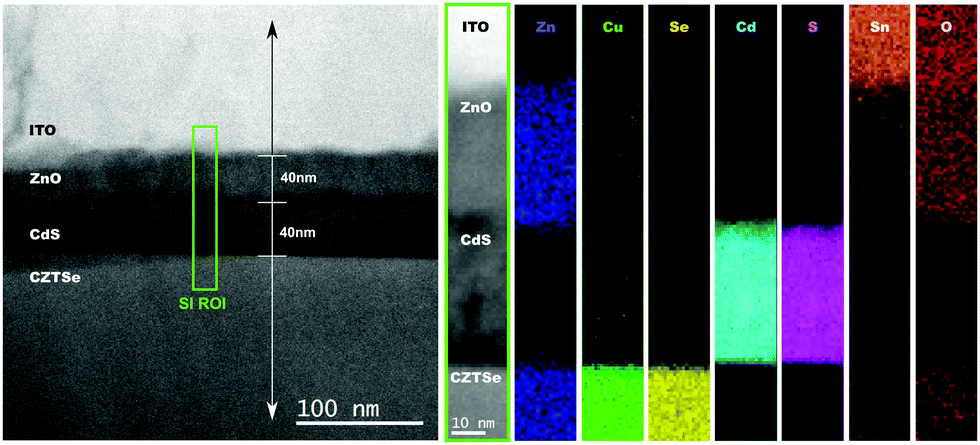 | ||
| Fig. 9 HAADF image of the front ITO/i-ZnO/CdS/CZTSe interfaces. Green box: region of the EELS scanning image. First stripe on the right: HAADF image of the area in the green box. Rest of stripes: elemental maps extracted from the EELS edges displayed in the top images. | ||
The front interface of the CZTSe device was further investigated by HRTEM images in cross-sectional and planar view configuration. Fig. 10a shows a cross-sectional image of the front interface between the CdS buffer layer and the CZTSe absorber in which both layers can be distinguished by the differences in contrast. FFTs (Fig. 10a.1–a.4) were performed to study the crystallinity of the sample on four different regions tagged as dashed squares in Fig. 10a: the CdS buffer layer, the CZTSe absorber, the CdS/CZTSe interface and the CdS/CZTSe interface area but displaced a few nanometres towards the CZTSe absorber. The distorted FFT pattern obtained for the CdS region is indicative of a very defective structure (Fig. 10a.1), expectable from a CBD-deposited thin film. The distortion spans down to the interface between the CdS and the CZTSe (Fig. 10a.2), which points out the presence of structural defects in this region as well. By displacing the area of the FFT analysis towards the absorber layer a few nanometres, a well-defined pattern arises in the [021] ZA (Fig. 10a.3). This pattern is almost identical to the one of the bulk of the absorber (Fig. 10a.4). The magnification of the HRTEM images covering the CdS/CZTSe interface reveals the existence of structural point and line defects both in the buffer layer and within the first nanometres of the front interface towards the CZTSe absorber (Fig. 10b and c).
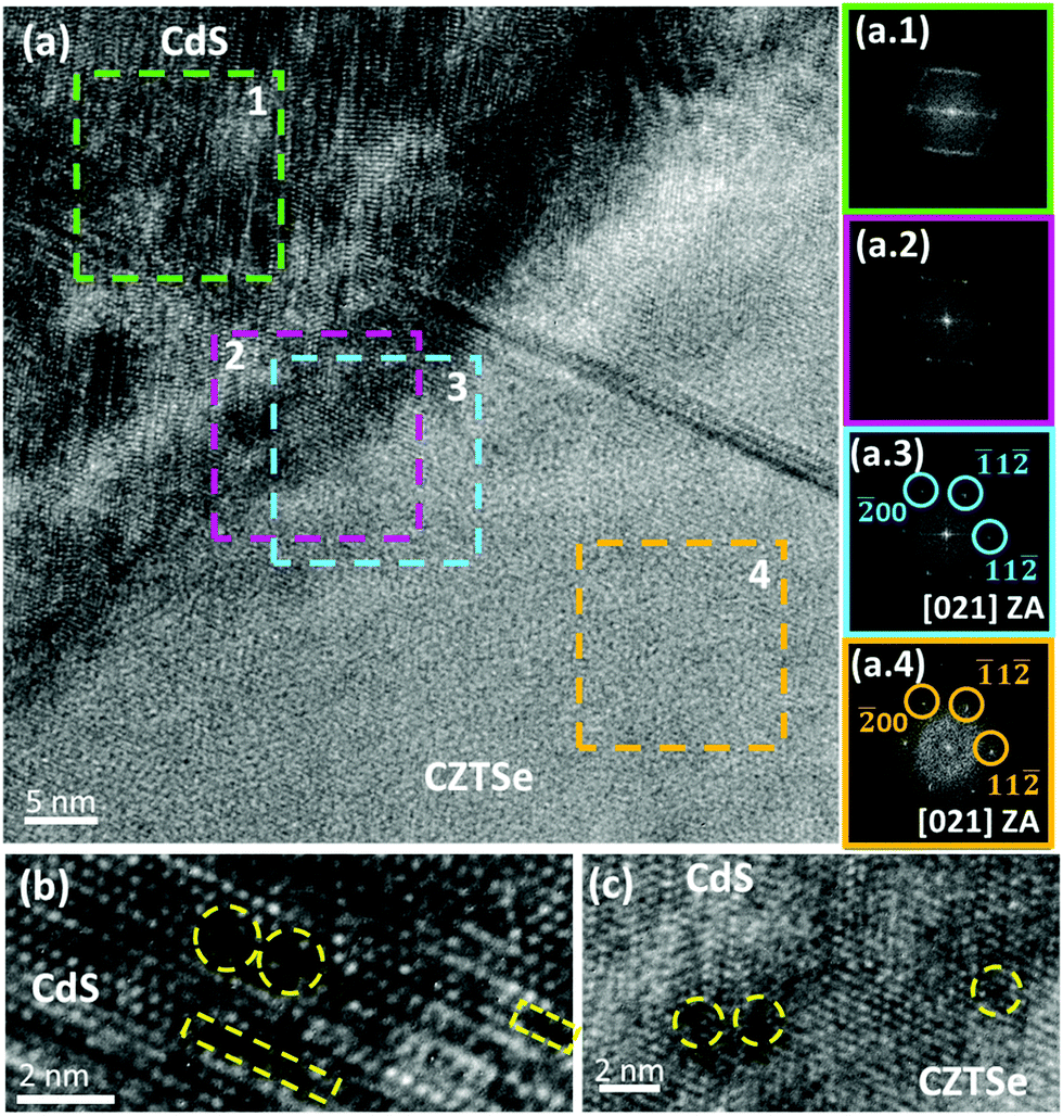 | ||
| Fig. 10 (a) Cross-sectional HRTEM image of the front interface between the CdS buffer layer and the CZTSe absorber. (a.1)–(a.4) FFT of the corresponding regions indicated by dashed rectangles in (a). ZA and three atomic planes are indicated in FFT with well-defined patterns. (b) Magnified cross-sectional HRTEM image of the CdS layer with highlighted point (dashed circles) and line defects (dashed rectangles). (c) Magnified cross-sectional HRTEM image of front interface between CdS and CZTSe with highlighted point defects. | ||
Planar view HRTEM images of the surface of the front interface of CZTSe absorber were acquired after removing the ITO/i-ZnO window layer and the CdS buffer layer by HCl etching and are shown in Fig. 11. Under high enough magnification, the images present multiple short narrow white lines distributed periodically over the surface. They can be attributed to line defects (one-dimensional defect). The periodicity of these defects indicates that they are not a by-product of sample preparation. Similar FFT patterns of areas containing these line defects and areas free of defects (Fig. 11a.1 and a.2) suggest that the line defects do not affect the crystal structure of the surrounding area. In addition, both patterns present the [021] ZA of the CZTSe structure, which means that the observed surface corresponds to CZTSe and, thus, that the ITO, i-ZnO and CdS layers were effectively removed. It can also be observed that the preferred orientation of the observed line defects is parallel to the (![[1 with combining macron]](https://www.rsc.org/images/entities/char_0031_0304.gif) 2) atomic plane. Magnified planar view HRTEM images of one line defect (Fig. 11b) reveal that the average length of all the observed line defects is about 9 nm. The orientation of the clearly resolved atomic planes does not change before and after the defect, in agreement with the similarity of the FFT patterns. However, some point defects can be observed in the area surrounding the line defect (marked with the dashed circle in Fig. 11b.2). These observations confirm the high density of defects at the front interface between CdS buffer layer and CZTSe absorber observed before in cross-sectional configuration. Fig. 11c shows planar view HRTEM images of the same area but obtained with different focus. The line defects almost disappear as the focus is changed towards the interior of absorber in depth so it can be concluded that these line defects are mainly concentrated at the surface (the remaining traces of the lines are probably related to the artefacts during the measurements). All these observations represent the first direct evidence of defect formation at the front interface of the absorber of kesterite-based PV devices measured in planar view configuration.
2) atomic plane. Magnified planar view HRTEM images of one line defect (Fig. 11b) reveal that the average length of all the observed line defects is about 9 nm. The orientation of the clearly resolved atomic planes does not change before and after the defect, in agreement with the similarity of the FFT patterns. However, some point defects can be observed in the area surrounding the line defect (marked with the dashed circle in Fig. 11b.2). These observations confirm the high density of defects at the front interface between CdS buffer layer and CZTSe absorber observed before in cross-sectional configuration. Fig. 11c shows planar view HRTEM images of the same area but obtained with different focus. The line defects almost disappear as the focus is changed towards the interior of absorber in depth so it can be concluded that these line defects are mainly concentrated at the surface (the remaining traces of the lines are probably related to the artefacts during the measurements). All these observations represent the first direct evidence of defect formation at the front interface of the absorber of kesterite-based PV devices measured in planar view configuration.
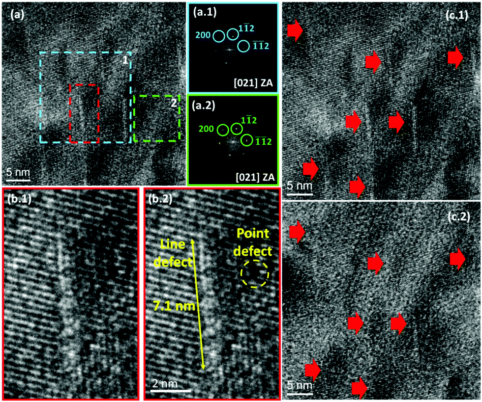 | ||
| Fig. 11 (a) Planar view HRTEM image of the front interface of the CZTSe device. A lower magnification image with the analysed area highlighted with a dashed rectangle can be found in Fig. S5 (ESI†). (a.1) and (a.2) FFT of the regions indicated by dashed rectangles in (a). The ZA and three atomic planes are indicated. (b) Magnified HRTEM image of the region indicated by a red dashed rectangle in (a), with (b.2) indication of dimensions of a line defect and highlighted point defect. (c) Planar view HRTEM images of the same area of the front interface obtained at different focus. The red arrows indicate dislocation defects. | ||
Finally, to complete the above presented analysis of the front interface of the absorber, impedance measurements were performed to estimate the carrier distribution throughout the space charge region (SCR). The measurements were performed in the solar cell with the highest efficiency and the data were treated by applying the equivalent circuit model consisting of a series resistor, a parallel resistor and a parallel capacitor55–57 (details on the capacitance derived from the impedance data analysis are presented in Fig. S4 (ESI†)). As a result, the dependence of the density of trapped and free carriers with the applied bias voltage was estimated (Fig. 12). It should be noted that an increase of the bias voltage results in a decrease of the width of the SCR. In these conditions, and considering that the SCR mainly lies in the absorber region of the solar cell, it is possible to assume that, at bias voltages >0 V, the carrier concentration will be more strongly influenced by the carriers present at the CdS/CZTSe interface. In these conditions, the drop of the density of free carriers and the increase of the density of trapped carriers at the bias voltage >0 V suggest the there is a higher density of trapping centres at the interface than in the bulk of the absorber. This finding is in accordance with the Raman and HRTEM observations, where a greater concentration of point and line structural defects was detected at the CdS/CZTSe interface.
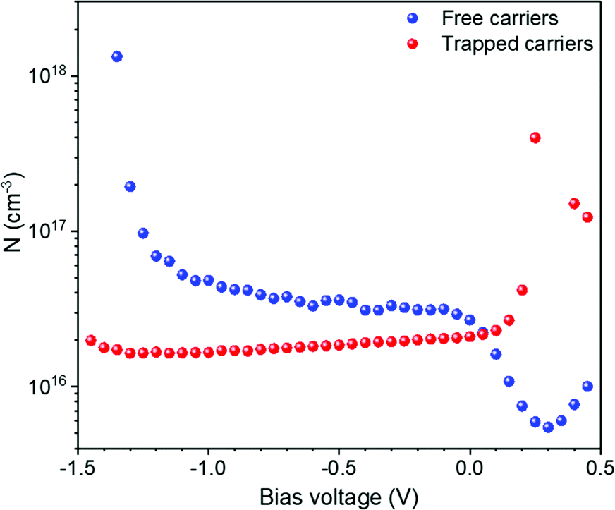 | ||
| Fig. 12 Dependencies of free and trapped carriers’ concentrations from the bias voltage. | ||
Discussion
In this section, the main results obtained in the different regions of the CZTSe device are discussed and employed to construct a full picture of possible factors that influence the performance of high efficiency kesterite devices with a focus on their Voc.The analysis of the CZTSe device has revealed that there is a considerable amount of voids, both micrometric and nanometric, at the back interface. Regarding the nanometric voids, they are not expected to have a noticeable influence on the performance of kesterite devices as their small size (< 50 nm) is significantly lower than the expected diffusion length of minority and majority carriers (>500 nm according to reported values).58,59 Oppositely, the large micrometric holes have been shown to decrease the contact area between the CZTSe absorber and the back contact by ∼40%. Consequently, the low diffusion length in CZTSe combined with these large voids undoubtedly hinders charge extraction at the back interface and lies at the origin of the large series resistance observed in the CZTSe device analysed in this work (see Fig. 2a). Although the large series resistance results in a low Jsc and FF in the analysed device,60 which is discussed in the Optoelectronic characterization section, it is not expected to have a significant influence in the Voc. However, besides affecting the back interface, the presence of holes has also been observed to lead to inhomogeneities in the thickness of the CZTSe absorber layer. Additionally, the thickness homogeneity of the active layer, and as result of the upper layers, is suffering from the relatively high roughness of the surface. A high surface roughness can increase the Jsc in PV devices since it increases the effective SCR of the device and, thus, increases light absorption and carrier generation.61 However, in this case, any possible benefit of an increased roughness is shadowed by the strong thickness variation of the absorber layer that results in a low effective thickness impeding an efficient absorption of NIR photons. This effect is in agreement with the observed low IQE of the device at the NIR region (Fig. 1b) and contributes, in addition to the series resistance, to its low Jsc. Similar effects in the Jsc and the IQE have been reported in absorber thinning studies in CIGS devices.62–65 In addition, the combination of large voids and thickness variations can produce fluctuations of the SCR width up to appearance of shunt paths that would limit the Voc of the device. The presence of areas with thickness below the width of the SCR can be clearly observed in the SEM image presented in Fig. 2. Finally, in the case of wider band gap kesterite absorbers, the variation in thickness and increased roughness can result in a higher front interface area that may aggravate CdS/CZTSe alignment-related interface recombination issues lowering the Voc and FF of the device.66 However, this should not affect the device analysed in this work since a favourable spike-like band alignment is expected between CZTSe and CdS.67
Regarding the origin of such large holes and thickness inhomogeneities, different possibilities can be considered. The first one is related to the well-known volatility of SnSe that, if formed at the back, would left voids behind after evaporation at the high temperatures employed for the synthesis of CZTSe.68 Another possibility would be that the voids originate upon the reaction of CZTSe with Mo as previously reported.36 However, the cross sectional images presented in this work suggest that the formation of voids may be somehow related to the observed bilayer absorber structure with small grains towards the back interface (see Fig. 2 and 3a). More specifically, it seems that some of the voids observed at the back interface arise from the absence of small grains at the bottom (Fig. 3a). This implies that the origin of the voids could be more fundamentally linked to the crystallization process and formation pathway of the CZTSe phase itself than to an “external cause”.
The combination of different transmission electron microscopy techniques for the analysis of bulk of the absorber has revealed that the analysed CZTSe device has a good crystalline quality, with kesterite type structure, very regular and well defined grain boundaries and without element inter-diffusion. These observations hint that the crystalline structure of the absorber bulk region is not the main origin of the Voc deficit in high efficiency CZTSe devices. However, despite the good crystal quality, both small grains in some back interface regions (as explained above) and twinning defects have been observed in the bulk of the absorber (see Fig. 3). Although the grain boundaries are generally considered as benign in CZTSe,69,70 a large density of horizontal grain boundaries and twinning defects could act as barriers that shorten the diffusion length of carriers and increase recombination in the bulk of the absorber. This would be reflected in the device as an increased series resistance, impacting the FF and Jsc.
The presence of voids and small grains at the back interface is not usually discussed or reported for high efficiency CZTSe devices.7,8,45,71,72 However, it seems that they are universal features of the kesterite technology since they can be observed even in kesterite devices with efficiencies beyond 12%.6,73 As such, it is difficult to come to a solid conclusion about and their real limiting effect on the optoelectronic properties of kesterite solar cells.
All the compositional measurements performed in this work point towards an overall Cu-poor Zn-rich homogeneous absorber composition. Nevertheless, the use of advanced spectroscopy techniques at the micro- and nanoscale has revealed slight inter-grain compositional variations. In particular, these were observed in cross-sectional configuration nanoXRF analysis and at the top interface of the absorber from AES and micro-Raman studies. All these slight compositional variations translate into changes in the intrinsic defect concentration and the preferential point defects in the CZTSe49,54 which, in turn, may cause grain-to-grain non-uniformity of the electrical and optical properties of the absorber. These changes may cause finally inhomogeneity in the performance of each individual grain and band fluctuation effects resulting in overall decrease of mainly Voc that is directly related to the intrinsic properties of the absorber. In addition, a slight inhomogeneity was observed in-depth by nanoXRF and UV-Raman. This indicates an increase of the Cu content in the bottom region and a reduction of the VCu defects. This gradient affects charge carrier mobility and recombination at the back interface. On the other hand, it should be noted that no evidence of secondary phases (except for MoSe2 at the back interface) has been found throughout the device so the compositional variations observed can be attributed solely to the kesterite phase. Finally, the inclusion of a Ge nanolayer in our standard process is a particularity of the present device (it is not the general procedure for the state of the art devices). Although the presence of residual Ge in the bulk of the absorber grains, mainly aggregated in the form of GeO2, has been proposed to contribute to recombination mechanisms,46 the reduced Ge layer thickness employed in our process results in a negligible effect in device performance. Furthermore, analyses of the influence of the Ge nanolayer on the bulk of the absorber concluded that it mainly affects the kesterite formation pathway leading to an improved crystalline properties and no effect in the interfaces has been observed.45,46,74 As such, the effect of the Ge nanolayer was mostly excluded from the evaluation and discussions presented in this work.
The formation of MoSe2 at the back interface has been confirmed by Raman and STEM. The latter has shown that the thickness of this layer is around 100 nm which can be considered to be in the optimum range and not have a detrimental effect on the device.38 However, Raman spectroscopy has revealed a difference in the relative intensity of the peaks of this layer in the absorber and substrate sides of the lifted-off samples. This is an indication of a different preferential structural orientation of MoSe2 on each side,53 and implies that this layer is really formed by two staked MoSe2 layers with different textures: one close to the back region of the absorber and the other one close to the Mo contact. Changes in the orientation of the c-axis (perpendicular or parallel to the substrate) of MoSe2 have been reported to have a relevant impact on the electrical and electronic properties of the back interface both for CuIn(S,Se)275 and CZTSe37 devices having a profound impact in the FF and Voc. Therefore, the double texture observed in the device analysed in this work is likely to be causing a strong anisotropy of the electrical and electronic properties of the back interface and, consequently, influencing the FF and Voc of the device.
The study of the front interface by HRTEM has revealed that there is a transitional region at the front interface of about 6 nm which is not so defective as the CdS buffer layer, but that has a worse crystalline quality than the bulk of the CZTSe absorber with a high density of line and point defects. These defects cover the full surface of the absorber and their appearance is in a great accordance with the presented Raman scattering results, which also showed a higher concentration of VCu and ZnSn point defects at the front interface of the absorber, and with the reduced concentration of free charge carriers observed by admittance spectroscopy. The line defects have been found to have a periodicity and a preferred orientation which implies that they are dislocations generated by stress relaxation. This means that there is an important stress at the front interface that is not present in the bulk of the absorber, which generates dislocations of the atomic planes that can act as recombination centres and affect the Voc of the device. The clear presence and higher density of defects encountered at the front interface suggests that this interface may be the main limitation for the Voc of the analysed device. The use of passivation layers at the front interface, or an etching technique to remove superficially these defects, could mitigate this issue. This has already been suggested in previous reports by applying a passivation Al2O3 layer,20,40,41 sulfurizing the CZTSe surface,39 and performing a surface oxygen plasma treatment.11
Finally, Cu–Zn disordering, usually pointed out as the main cause of the Voc deficit in kesterites27,76,77 was not described in the present study. Unfortunately, the EELS measurements carried out in this work did not allow an atomic-resolved analysis. Thus, it was not possible to determine which specific element corresponds to each atom resolved in the HAADF images (Fig. 4). As such, Cu–Zn disordering is likely to have a significant influence in the Voc deficit of the device analysed in this work although no concluding proof of this can be provided.
Based on the presented findings and their possible influence on kesterite devices, it is possible to point out several issues that could be addressed as a general roadmap to overcome the existing efficiency limitations of the kesterite technology. Firstly, the development of a strict fabrication process focused on a high reproducibility would minimize some of the well-known and widely discussed problems typically found in kesterite absorbers such as secondary phases, low crystalline quality and compositional inhomogeneities as well as those observed in this work such as the twining defects, and double layer structure of the grains. However, at the current level of development of the technology, the appearance of inhomogeneity problems is mostly unavoidable and seems a fundamental property of kesterites due to their high compositional flexibility that allows a high degree of stoichiometric and structural fluctuations.49 Nevertheless, we strongly believe that slight compositional and structural inhomogeneities may just have a residual effect on device performance at the current level of development of the technology in comparison to the problems located at the interfaces. Regarding the back interface, the development of strategies that ensure a good element intermixing and favor a formation pathway that avoids the formation of volatile phases (see ref. 42, 74 and 78) could minimize the appearance of large voids. As for the front interface, the distorted region with increased amount of point and line defects found in this work could be eliminated employing specific passivation or etching strategies (see ref. 17 and 40) as well as by researching on alternative materials and deposition techniques for the buffer layer that have better band and structural alignment with the kesterite absorber.
Conclusions
The combination of advanced electron microscopy and spectroscopy techniques at the macro, micro and nanoscale has enabled to carry out a deep analysis of defect formation in a high efficiency CZTSe device. The work has tackled the simultaneous investigation of the bulk and the front and back interfaces to assess the impact on the performance of the defects found in each part of the device. Table 2 summarizes the main findings identified in this work as potential issues, their location within the device, the technique employed to detect them and their possible influence on device performance. The study of the bulk has revealed large absorber thickness variations that reduce NIR photon absorption and increase the probability of shunting. On the other hand, a good crystalline quality, homogeneous composition and well-defined grain boundaries have been observed in the bulk of the absorber. However, the analysis has also revealed the formation of a bilayer structure with small grains at the bottom and of twinning defects that could act as barriers leading to recombination. Voids have been observed at the back interface decreasing the contact area between CZTSe and Mo and leading to a high series resistance in the device. Finally, a high density of defects and grain-to-grain non-uniformities have been observed at the front interface. The defective area covers the full surface of the absorber and extends from the CdS/CZTSe interface towards the first 6 nm of the absorber with a high presence of line and point defects. These results point towards the front interface being the main source of Voc deficit of the device. Nevertheless, the issues observed in the bulk and back interface also represent important and comparable drawbacks for device performance. This work has provided, for the first time, direct evidence of twinning defects in the bulk, micro and nano-voids at the back interface and of the widely-suspected high density of defects at the front interface. This represents a step forward in the comprehension of the main limitations of the kesterite solar cells and opens the way to the identification of new solutions to further developing this technology and pushing it towards higher performances.| Device layer | Findings | Technique | Main possible influence on device performance |
|---|---|---|---|
| a Issues of the kesterite absorbers found or clearly observed for the first time. | |||
| CZTSe/CdS front interface | VCu and ZnSn point defects | Macro-Raman spectroscopy | Control P-type doping, act as recombination centres and affect Voc device |
| Grain-to-grain non-uniformitya | Micro-Raman spectroscopy, AES | Contribution in band fluctuations impacting in the Voc | |
| ∼6 nm depth distorted regiona, point and line structural defectsa | Cross-sectional & planar view HRTEM | Recombination in the space charge region, reduction of Voc | |
| Decrease of the density of free charge carriers | Admittance spectroscopy | Reduction of Jsc | |
| CZTSe bulk | Good crystalline quality grains & well defined grain boundaries | Cross-sectional HRTEM | Good carrier mobility |
| Twinning defectsa | Cross-sectional HRTEM | Bulk recombination centres affecting FF and Jsc | |
| Thickness inhomogeneity | Cross-sectional HRTEM and SEM | Space charge region fluctuation, shunting, decrease Jsc due to reduce absorption of NIR photons | |
| Bilayer structure (small grains in the bottom) | Cross-sectional HRTEM and SEM | Bulk recombination centres affecting FF and Jsc | |
| Slightly in-depth compositional inhomogeneity | nanoXRF | Impact in the mobility and recombination of charge carriers | |
| Mo/MoSe2/CZTSe back interface | ∼100 nm MoSe2 thickness | Cross-sectional TEM | Favourable thickness for ohmic back contact |
| Bilayer structure of MoSe2 layera | Raman spectroscopy | Influences in electrical properties in the back contact, FF and Voc | |
| Voids | Planar view SEM & cross-sectional TEM | Shunting, decrease back contact area, reduction of FF and Jsc, reduction of the NIR photon absorption, decrease Jsc | |
Experimental
The high-efficiency CZTSe solar cell device analysed in this work was fabricated through a sequential process. First, a Cu/Sn/Cu/Zn metallic stack precursor was deposited by DC magnetron sputtering (Alliance Concept Ac540) onto a Mo coated soda lime glass (SLG) substrate. The thickness of the different layers of the stack was selected to obtain a Cu-poor Zn-rich composition with [Cu]/([Zn] + [Sn]) = 0.73 and [Zn]/[Sn] = 1.11 as measured macroscopically by XRF (Fisherscope XDV-SDD). A 10 nm Ge nanolayer was evaporated (Oerlikon Univex 250) on top of the precursor mainly to control the formation pathway as previously described in ref. 45 and 74. The metallic precursor was then reactively annealed under a Se + Sn atmosphere to form the CZTSe absorber, and several chemical etching treatments were applied to remove selectively secondary phases and to passivate the surface as reported elsewhere.74 The solar cell was completed with a CdS buffer layer deposited by chemical bath deposition with reduced layer growth kinetics based on the use of cadmium nitrate precursor salts as described elsewhere.67 The deposition of the buffer layer was followed by pulsed DC magnetron sputtering (Alliance Concept CT100) deposition of i-ZnO and In2O3–SnO2 (ITO) window layers. The different layers composing the complete device are depicted in Fig. 13 (left). Individual 3 × 3 mm2 solar cells were mechanical scribed employing a manual microdiamond scriber (OEG MR200).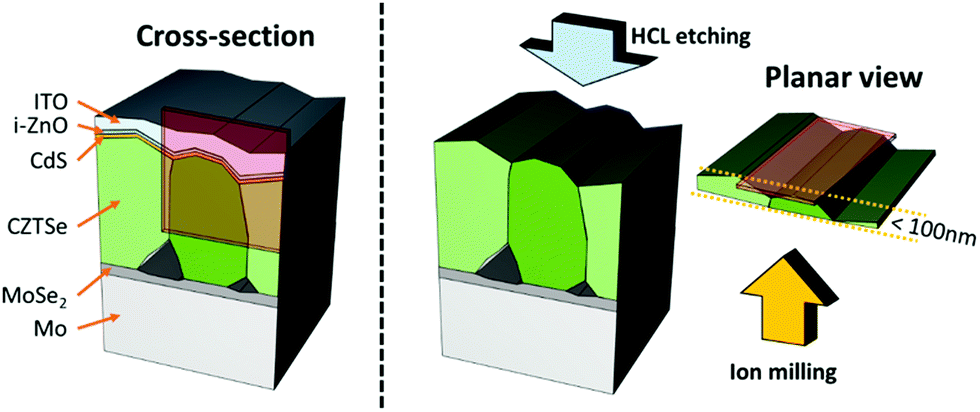 | ||
| Fig. 13 Schematic representation of the sample preparation for cross-section (left) and planar (right) view STEM geometries. The observation planes are highlighted with red rectangles. For planar view geometry, the direction of HCl etching to remove CdS, i-ZnO and ITO layers, and of the ion milling to thin down the CZTSe absorber are indicated with a blue and yellow arrow, respectively. | ||
The J–V characteristics of the devices were obtained under simulated AM1.5 illumination using a pre-calibrated Sun 3000 Class AAA solar simulator (Abet Technologies). The EQE, IQE and reflectance of the solar cells were measured using a spectral response system (Bentham PVE300) calibrated with Si and Ge photodiodes. The electronic properties of the solar cells were characterized by impedance spectroscopy using a Keysight E4990A Impedance Analyzer. Impedance measurements were carried out at room temperature in dark conditions with a 50 mV alternating current (AC) signal over 40 AC frequency steps (from 20 Hz to 10 MHz), and 41 bias voltage steps (from −1.5 V to 0.5 V). The frequency range was stablished in accordance to the limitations of the system, while the voltage range was determined by the Voc of the device and signal-to-noise ratio criteria. The number of steps was selected to allow a proper calculation of the first derivatives of capacitances C(ω) and C(V).
The morphology at the micro and nanoscales was investigated by SEM, and several configurations of TEM: STEM, HRTEM and HAADF. The use of different electron microscopy techniques and imaging modes allows focusing on different characteristics of the absorber at different scales. In this way, SEM and STEM images were mainly used for an overall view of the device at a microlevel, for investigation absorber grains and voids, and for selecting interesting regions for further deeper analysis. Subsequently, HRTEM and HAADF provided results about the structural and compositional properties of the absorber and the interfaces at the nanoscale. All these techniques were used both in cross-sectional and planar view configuration as presented in Fig. 13. Regarding the cross-sectional sample preparation for TEM, FIB was used. A platinum nanolayer was deposited onto the sample to protect its surface from the aggressive FIB etching process. On the other hand, the planar view required a carefully adjusted sample preparation (see Fig. S6 (ESI†)) that, to the best of our knowledge, has not been previously reported for kesterite based devices. This preparation started with the removal of the ITO, i-ZnO and CdS layers by submitting the sample to a chemical etching in HCl (5% v/v). Then, the etched sample was cut with a filament diamond saw into 3 mm thick (including the SLG substrate) 2.5 × 2.5 mm2 pieces. These pieces were then polished from the substrate side to preserve the front interface surface (see Fig. 13, right). A first polishing was carried out with a series of diamond abrasive films with decreasing grain sizes (30, 15, 6, 1 and 0.5 μm), a until the samples were thinned down to 30–70 μm. Then, a final thinning (down to a thickness < 50 nm) was performed by ion milling tripod polisher kit (model 590, South Bay Technologies) and a 12′′ metallographic manual polisher (NANO 1200T, Pace Technologies) using a Fischione 1010 Precision Ion Polishing System with the upper source working at 5.0 kV and 5.0 mA. Although the mechanical polishing approach was successfully implemented for the planar view preparation, some difficulties are worth mentioning. For instance, the CZTSe multilayer overall thickness complicated the thinning process down to the electron transparency range. Furthermore, the observable area was small since, being a granular sample, the CZTSe thin foil resulted extremely brittle and some sections were easily damaged when handling, but without affecting the remaining electro-transparent regions.
SEM images were obtained with a ZEISS Series Auriga microscope using 5 kV accelerating voltage. The HRTEM planar view images were acquired in a JEOL-2100 with a LaB6 filament at 200 keV. The HRTEM and low magnification DF-BF cross-sectional images were acquired in a JEOL-2010F with a field emission gun at 200 keV. The high resolution HAADF (STEM) images and EELS spectrum images were acquired in a JEOL-ARM-F with field emission gun at 200 keV (FEG electron source and Cs aberration correction in the condenser lens system). The obtained images were analysed through a combination of Gatan Digital Micrograph proprietary software and Hyperspy (Python-based) free software. CaRIne Crystallography and TEM-UCA EJE-Z79 were also used to identify the crystalline structures.80
Raman spectroscopy was employed to analyse the presence of secondary phases and point defects in the macro scale at the front (after a chemical removing the top layers with an etching in 5% v/v HCl) and back (after detaching the absorber from the substrate through a mechanical lift-off process, see Fig. S7 (ESI†)) interfaces. A FHR640 Horiba Jobin Yvon spectrometer coupled to a Raman probe developed at IREC and a CCD detector cooled to −70 °C was used. Laser excitation wavelengths of 325 and 532 nm were employed in backscattering configuration. A laser power density of about 50 W cm−2 was used to prevent thermal effects on the samples and the diameter of the laser macro-spot was around 70 μm. The Raman shift was calibrated using a monocrystalline Si reference by imposing the position of its main peak to be at 520 cm−1. An unpolarised laser beam was used to minimize the impact of the crystalline orientation in the Raman spectra.
Mappings of the defect distribution at the microscale were performed at the front interface of the absorber by micro-Raman spectroscopy using a LabRam spectrometer (Horiba Jobin Yvon) coupled with a CCD. The measurements were performed in a backscattering configuration under a 532 nm excitation wavelength. An Olympus metallographic microscope was used to allow the concentration of the measurement spot down to 1 μm. The laser power did not exceed 1 mW. A high precision XY-stage was used to manipulate the sample and enable mapping a 20 × 20 μm2 area. Auger electron spectroscopy (AES) was performed at the front interface of the absorber in similar area to study the compositional homogeneity at the nanoscale using a PHI 670 Scanning Auger Microscope from Physical Electronics. The Auger spectra were acquired using a FE electron source working at 10 keV and 10 nA. The mappings were performed in UHV (below 10−10 Torr) and measurements were done using a point spot (diameter around 50 nm) with an estimated penetration depth in the range of 1 to 3 nm. To remove the signal corresponding to adventitious carbon and native surface oxidation that occurs on a surface exposed to air, a 3.5 keV light Ar+ ion surface sputtering of ∼2 nm was performed previously to the measurements. Multipak version 9.9.08 software from ULVAC-PHI was used for data treatment of the signal for the different cations.
The composition throughout the bulk of the absorber was analyzed by nanoXRF on a cross-sectional lamella prepared using a FIB. The nanoXRF measurements were performed in spot analysis and mapping mode at the nano-analysis beamline ID16B of the European Synchrotron Radiation Facility (ESRF) in Grenoble, France.81 The X-ray energy was set to 29.6 keV in “pink-beam” mode with a focal spot size of 54 × 52 nm2 and an average flux of 2.5 × 10¹⁰ photons per s. The lamella was raster scanned through the nano-beam with a step size of 50 nm in the vertical and horizontal directions. Detecting the emitted X-ray fluorescence radiation for each position by two 3-element silicon drift detectors, and fitting the respective spectra, provides compositional information for each individual spot.46 Finally, electron energy-loss spectroscopy (EELS) (GIF Quantum EF spectrometer attached to JEOL-ARM-F) was used to study interlayer element diffusion at the front interface.
Conflicts of interest
There are no conflicts to declare.Acknowledgements
The authors acknowledge the ESRF for provision of synchrotron radiation (experiment: MA-3564). This research was partially supported by the H2020 Programme under the project INFINITE-CELL (H2020-MSCA-RISE-2017-777968), by the In4CIS project from the SOLAR-ERA.NET International program (subproject ref. PCIN-2018-48), and by the Spanish Ministry of Science, Innovation and Universities under the FOTOSENS project (RTC-2017-5857-3). Part of this work was financially supported by the German Federal Ministry of Education and Research under the nano@work project (contract number: 05K16SJ1) and by the Deutsche Forschungsgemeinschaft (DFG, German Research Foundation) under the project number SCHN 1283/2-1. Authors from IREC and the University of Barcelona belong to the SEMS (Solar Energy Materials and Systems) Consolidated Research Group of the “Generalitat de Catalunya” (Ref. 2017 SGR 862), and acknowledge the support of the European Regional Development Funds (ERDF, FEDER Programa Competitivitat de Catalunya 2007–2013). Other UB authors belong to the Consolidated Research Group of the “Generalitat de Catalunya” MIND (Micro-nanotechnology and nanoscopies for electronic and photonic devices) (Ref. 2017 SGR 776) and acknowledge funding from the Spanish Ministery through the research project MAT2017-79455-P and research network RED2018-102609-T. M. P. and M. G. thanks the Government of Spain for the Ramon y Cajal (RYC-2017-23758) and Juan de la Cierva (IJC2018-038199-I) Fellowships, respectively.References
- First Solar, First Solar Achieves Yet Another Cell Conversion Efficiency World Record, http://www.pes.eu.com/renewable-news/first-solar-achieves-yet-another-cell-conversion-efficiency-world-record/, accessed June 2020.
- Solar Frontier, Solar Frontier Achieves World Record Thin-Film Solar Cell Efficiency of 23.35%, http://www.solarfrontier. com/eng/news/2019/0117_press.html, accessed June 2020.
- C. Candelise, M. Winskel and R. Gross, Prog. Photovoltaics, 2012, 20, 816–831 Search PubMed.
- A. Feltrin and A. Freundlich, Renewable Energy, 2008, 33, 180–185 CrossRef CAS.
- G. Phipps, C. Mikolajczak and T. Guckes, Indium and Gallium: long-term supply, http://www.renewableenergyfocus.com/view/3322/indium-and-gallium-long-term-supply/, accessed June 2020.
- W. Wang, M. T. Winkler, O. Gunawan, T. Gokmen, T. K. Todorov, Y. Zhu and D. B. Mitzi, Adv. Energy Mater., 2014, 4, 1301465 CrossRef.
- Z. Su, G. Liang, P. Fan, J. Luo, Z. Zheng, Z. Xie, W. Wang, S. Chen, J. Hu, Y. Wei, C. Yan, J. Huang, X. Hao and F. Liu, Adv. Mater., 2020, 32, 2000121 CrossRef CAS.
- X. Li, D. Zhuang, N. Zhang, M. Zhao, X. Yu, P. Liu, Y. Wei and G. Ren, J. Mater. Chem. A, 2019, 7, 9948–9957 RSC.
- T. Feurer, R. Carron, G. Torres Sevilla, F. Fu, S. Pisoni, Y. E. Romanyuk, S. Buecheler and A. N. Tiwari, Adv. Energy Mater., 2019, 9, 1901428 CrossRef.
- J. AbuShama, R. Noufi, S. Johnston, S. Ward and X. Wu, in Conference Record of the Thirty-first IEEE Photovoltaic Specialists Conference, 2005, IEEE, pp. 299–302.
- H. Tampo, S. Kim, T. Nagai, H. Shibata and S. Niki, ACS Appl. Mater. Interfaces, 2019, 11, 13319–13325 CrossRef CAS.
- O. Gunawan, T. K. Todorov and D. B. Mitzi, Appl. Phys. Lett., 2010, 97, 233506 CrossRef.
- D. A. R. Barkhouse, O. Gunawan, T. Gokmen, T. K. Todorov and D. B. Mitzi, Prog. Photovoltaics, 2012, 20, 6–11 CAS.
- J. J. Scragg, T. Ericson, X. Fontané, V. Izquierdo-Roca, A. Pérez-Rodríguez, T. Kubart, M. Edoff and C. Platzer-Björkman, Prog. Photovoltaics, 2014, 22, 10–17 CAS.
- Y. Zhao, X. Han, B. Xu, W. Li, J. Li, J. Li, M. Wang, C. Dong, P. Ju and J. Li, IEEE J. Photovolt., 2017, 7, 874–881 Search PubMed.
- Z.-K. Yuan, S. Chen, H. Xiang, X.-G. Gong, A. Walsh, J.-S. Park, I. Repins and S.-H. Wei, Adv. Funct. Mater., 2015, 25, 6733–6743 CrossRef CAS.
- H. Xie, Y. Sáncheza, P. Tang, M. Espíndola-Rodríguez, M. Guc, L. Calvo-Barrio, S. López-Marino, Y. Liu, J. R. Morante, A. Cabot, V. Izquierdo-Roca, J. Arbiol, A. Pérez-Rodríguez and E. Saucedo, Sol. RRL, 2019, 3, 1800279 Search PubMed.
- Y. Sánchez, M. Espíndola-Rodríguez, H. Xie, S. López-Marino, M. Neuschitzer, S. Giraldo, M. Dimitrievska, M. Placidi, V. Izquierdo-Roca, F. A. Pulgarín-Agudelo, O. Vigil-Galán and E. Saucedo, Sol. Energy Mater. Sol. Cells, 2016, 158, 138–146 CrossRef.
- L. Yin, G. Cheng, Y. Feng, Z. Li, C. Yang and X. Xiao, RSC Adv., 2015, 5, 40369–40374 RSC.
- M. E. Erkan, V. Chawla and M. A. Scarpulla, J. Appl. Phys., 2016, 119, 194504 CrossRef.
- S. López-Marino, Y. Sánchez, M. Placidi, A. Fairbrother, M. Espindola-Rodríguez, X. Fontané, V. Izquierdo-Roca, J. López-García, L. Calvo-Barrio, A. Pérez-Rodríguez and E. Saucedo, Chem. – Eur. J., 2013, 19, 14814–14822 CrossRef.
- Y. Zhao, X. Han, L. Chang, J. Li, C. Dong, Y. Fang and J. Li, Sol. Energy Mater. Sol. Cells, 2018, 179, 427–434 CrossRef CAS.
- S. Chen, A. Walsh, X.-G. Gong and S.-H. Wei, Adv. Mater., 2013, 25, 1522–1539 CrossRef CAS.
- S. Schorr, Sol. Energy Mater. Sol. Cells, 2011, 95, 1482–1488 CrossRef CAS.
- M. Paris, L. Choubrac, A. Lafond, C. Guillot-Deudon and S. Jobic, Inorg. Chem., 2014, 53, 8646–8653 CrossRef CAS.
- G. Rey, G. Larramona, S. Bourdais, C. Choné, B. Delatouche, A. Jacob, G. Dennler and S. Siebentritt, Sol. Energy Mater. Sol. Cells, 2018, 179, 142–151 CrossRef CAS.
- T. Gokmen, O. Gunawan, T. K. Todorov and D. B. Mitzi, Appl. Phys. Lett., 2013, 103, 103506 CrossRef.
- M. Neuschitzer, Y. Sanchez, T. Olar, T. Thersleff, S. Lopez-Marino, F. Oliva, M. Espindola-Rodriguez, H. Xie, M. Placidi, V. Izquierdo-Roca, I. Lauermann, K. Leifer, A. Pérez-Rodriguez and E. Saucedo, Chem. Mater., 2015, 27, 5279–5287 CrossRef CAS.
- G. Rey, A. Redinger, J. Sendler, T. P. Weiss, M. Thevenin, M. Guennou, B. El Adib and S. Siebentritt, Appl. Phys. Lett., 2014, 105, 112106 CrossRef.
- H. Xie, Y. Sánchez, S. López-Marino, M. Espíndola-Rodríguez, M. Neuschitzer, D. Sylla, A. Fairbrother, V. Izquierdo-Roca, A. Pérez-Rodríguez and E. Saucedo, ACS Appl. Mater. Interfaces, 2014, 6, 12744–12751 CrossRef CAS.
- I. Becerril-Romero, L. Acebo, F. Oliva, V. Izquierdo-Roca, S. López-Marino, M. Espíndola-Rodríguez, M. Neuschitzer, Y. Sánchez, M. Placidi, A. Pérez-Rodríguez, E. Saucedo and P. Pistor, Prog. Photovoltaics, 2018, 26, 55–68 CAS.
- T. Schwarz, O. Cojocaru-Mirédin, P. Choi, M. Mousel, A. Redinger, S. Siebentritt and D. Raabe, J. Appl. Phys., 2015, 118, 095302 Search PubMed.
- K. Sardashti, R. Haight, T. Gokmen, W. Wang, L.-Y. Chang, D. B. Mitzi and A. C. Kummel, Adv. Energy Mater., 2015, 5, 1402180 CrossRef.
- I. L. Repins, H. Moutinho, S. G. Choi, A. Kanevce, D. Kuciauskas, P. Dippo, C. L. Beall, J. Carapella, C. DeHart, B. Huang and S. H. Wei, J. Appl. Phys., 2013, 114, 084507 CrossRef.
- J. J. Scragg, J. T. Wätjen, M. Edoff, T. Ericson, T. Kubart and C. Platzer-Björkman, J. Am. Chem. Soc., 2012, 134, 19330–19333 CrossRef CAS.
- S. López-Marino, M. Placidi, A. Pérez-Tomás, J. Llobet, V. Izquierdo-Roca, X. Fontané, A. Fairbrother, M. Espíndola-Rodríguez, D. Sylla, A. Pérez-Rodríguez and E. Saucedo, J. Mater. Chem. A, 2013, 1, 8338–8343 RSC.
- S. Lopez-Marino, M. Espíndola-Rodríguez, Y. Sánchez, X. Alcobé, F. Oliva, H. Xie, M. Neuschitzer, S. Giraldo, M. Placidi, R. Caballero, V. Izquierdo-Roca, A. Pérez-Rodríguez and E. Saucedo, Nano Energy, 2016, 26, 708–721 CAS.
- B. Shin, Y. Zhu, N. A. Bojarczuk, S. Jay Chey and S. Guha, Appl. Phys. Lett., 2012, 101, 053903 CrossRef.
- S. Wang, S. Gao, D. Wang, Z. Jiang, J. Ao, Z. Zhou, S. Liu, Y. Sun and Y. Zhang, Sol. RRL, 2019, 3, 1800236 CrossRef.
- E. Ojeda-Durán, K. Monfil-Leyva, J. Andrade-Arvizu, I. Becerril-Romero, Y. Sánchez, R. Fonoll-Rubio, M. Guc, Z. Jehl, J. A. Luna-López, A. L. Muñoz-Zurita, J. A. D. Hernández-de la Luz, V. Izquierdo-Roca, M. Placidi and E. Saucedo, Sol. Energy, 2020, 198, 696–703 CrossRef.
- J. Kim, S. Park, S. Ryu, J. Oh and B. Shin, Prog. Photovoltaics, 2017, 25, 308–317 CAS.
- T. Gershon, B. Shin, N. Bojarczuk, M. Hopstaken, D. B. Mitzi and S. Guha, Adv. Energy Mater., 2015, 5, 1400849 CrossRef.
- L. Grenet, M. A. A. Suzon, F. Emieux and F. Roux, ACS Appl. Energy Mater., 2018, 1, 2103–2113 CrossRef CAS.
- S. Giraldo, Z. Jehl, M. Placidi, V. Izquierdo-Roca, A. Pérez-Rodríguez and E. Saucedo, Adv. Mater., 2019, 31, 1806692 CrossRef.
- S. Giraldo, E. Saucedo, M. Neuschitzer, F. Oliva, M. Placidi, X. Alcobé, V. Izquierdo-Roca, S. Kim, H. Tampo, H. Shibata, A. Pérez-Rodríguez and P. Pistor, Energy Environ. Sci., 2018, 11, 582–593 CAS.
- M. Ritzer, S. Schönherr, P. Schöppe, W. Wisniewski, S. Giraldo, G. Gurieva, A. Johannes, C. T. Plass, K. Ritter, G. Martínez-Criado, S. Schorr, E. Saucedo, C. Ronning and C. S. Schnohr, ACS Appl. Energy Mater., 2020, 3, 558–564 CrossRef CAS.
- S. Chen, X. G. Gong, A. Walsh and S.-H. Wei, Appl. Phys. Lett., 2009, 94, 041903 CrossRef.
- P. Schöppe, S. Schönherr, P. Jackson, R. Wuerz, W. Wisniewski, M. Ritzer, M. Zapf, A. Johannes, C. S. Schnohr and C. Ronning, ACS Appl. Mater. Interfaces, 2018, 10, 40592–40598 CrossRef.
- S. Schorr, G. Gurieva, M. Guc, M. Dimitrievska, A. Pérez-Rodríguez, V. Izquierdo-Roca, C. S. Schnohr, J. Kim, W. Jo and J. M. Merino, J. Phys. Energy, 2020, 2, 012002 CrossRef CAS.
- M. Dimitrievska, F. Oliva, M. Guc, S. Giraldo, E. Saucedo, A. Pérez-Rodríguez and V. Izquierdo-Roca, J. Mater. Chem. A, 2019, 7, 13293–13304 RSC.
- M. Dimitrievska, S. Giraldo, P. Pistor, E. Saucedo, A. Pérez-Rodríguez and V. Izquierdo-Roca, Sol. Energy Mater. Sol. Cells, 2016, 157, 462–467 CrossRef CAS.
- M. Dimitrievska, A. Fairbrother, E. Saucedo, A. Pérez-Rodríguez and V. Izquierdo-Roca, Sol. Energy Mater. Sol. Cells, 2016, 149, 304–309 CAS.
- T. Sekine, M. Izumi, T. Nakashizu, K. Uchinokura and E. Matsuura, J. Phys. Soc. Jpn., 1980, 49, 1069–1077 CrossRef CAS.
- L. E. Valle Rios, K. Neldner, G. Gurieva and S. Schorr, J. Alloys Compd., 2016, 657, 408–413 CrossRef CAS.
- H.-S. Kim, D. B. Patel, H. Kim, M. Patel, K. R. Chauhan, W. Park and J. Kim, Sol. Energy Mater. Sol. Cells, 2017, 164, 7–12 CAS.
- R. Bodeux, J. Rousset, F. Tsin, F. Mollica, E. Leite and S. Delbos, Appl. Phys. A: Mater. Sci. Process., 2018, 124, 22 CrossRef.
- J. T. Heath, J. D. Cohen and W. N. Shafarman, J. Appl. Phys., 2004, 95, 1000–1010 CrossRef CAS.
- H. Hempel, A. Redinger, I. Repins, C. Moisan, G. Larramona, G. Dennler, M. Handwerg, S. F. Fischer, R. Eichberger and T. Unold, J. Appl. Phys., 2016, 120, 175302 Search PubMed.
- C. J. Hages, A. Redinger, S. Levcenko, H. Hempel, M. J. Koeper, R. Agrawal, D. Greiner, C. A. Kaufmann and T. Unold, Adv. Energy Mater., 2017, 7, 1700167 CrossRef.
- V. Karade, A. Lokhande, P. Babar, M. G. Gang, M. Suryawanshi, P. Patil and J. H. Kim, Sol. Energy Mater. Sol. Cells, 2019, 200, 109911 CrossRef CAS.
- Z. Jehl, M. Bouttemy, D. Lincot, J. F. Guillemoles, I. Gerard, A. Etcheberry, G. Voorwinden, M. Powalla and N. Naghavi, J. Appl. Phys., 2012, 111, 114509 CrossRef.
- E. Leonard, L. Arzel, M. Tomassini, P. Zabierowski, D. Fuertes Marrón and N. Barreau, J. Appl. Phys., 2014, 116, 074512 CrossRef.
- Z. Jehl, F. Erfurth, N. Naghavi, L. Lombez, I. Gerard, M. Bouttemy, P. Tran-Van, A. Etcheberry, G. Voorwinden, B. Dimmler, W. Wischmann, M. Powalla, J. F. Guillemoles and D. Lincot, Thin Solid Films, 2011, 519, 7212–7215 CrossRef CAS.
- H. Heriche, Z. Rouabah and N. Bouarissa, Int. J. Hydrogen Energy, 2017, 42, 9524–9532 CrossRef CAS.
- L. Grenet, F. Emieux, O. Dellea, A. Gerthoffer, G. Lorin, F. Roux and S. Perraud, Thin Solid Films, 2017, 621, 188–194 CrossRef CAS.
- K. Beom Cheon, S. K. Hwang, S. W. Seo, J.-H. Park, M.-A. Park and J. Y. Kim, ACS Appl. Mater. Interfaces, 2019, 11, 24088–24095 CrossRef.
- M. Neuschitzer, Y. Sanchez, S. López-Marino, H. Xie, A. Fairbrother, M. Placidi, S. Haass, V. Izquierdo-Roca, A. Perez-Rodriguez and E. Saucedo, Prog. Photovoltaics, 2015, 23, 1660–1667 CAS.
- J. J. Scragg, P. J. Dale, D. Colombara and L. M. Peter, ChemPhysChem, 2012, 13, 3035–3046 CrossRef CAS.
- J. B. Li, V. Chawla and B. M. Clemens, Adv. Mater., 2012, 24, 720–723 CAS.
- G. Y. Kim, A. R. Jeong, J. R. Kim, W. Jo, D.-H. Son, D.-H. Kim and J.-K. Kang, Sol. Energy Mater. Sol. Cells, 2014, 127, 129–135 CrossRef CAS.
- T. Taskesen, J. Neerken, J. Schoneberg, D. Pareek, V. Steininger, J. Parisi and L. Gütay, Adv. Energy Mater., 2018, 8, 1703295 CrossRef.
- Y. S. Lee, T. Gershon, O. Gunawan, T. K. Todorov, T. Gokmen, Y. Virgus and S. Guha, Adv. Energy Mater., 2015, 5, 1401372 CrossRef.
- S.-Y. Kim, S.-H. Kim, S. Hong, D.-H. Son, Y.-I. Kim, S. Kim, K. Ahn, K.-J. Yang, D.-H. Kim and J.-K. Kang, ACS Appl. Mater. Interfaces, 2019, 11, 23160–23167 CrossRef CAS.
- S. Giraldo, M. Neuschitzer, T. Thersleff, S. López-Marino, Y. Sánchez, H. Xie, M. Colina, M. Placidi, P. Pistor, V. Izquierdo-Roca, K. Leifer, A. Pérez-Rodríguez and E. Saucedo, Adv. Energy Mater., 2015, 5, 1501070 CrossRef.
- C. M. Ruiz, A. Pérez-Rodríguez, J. Arbiol, J. R. Morante and V. Bermúdez, Phys. Status Solidi, 2015, 212, 61–66 CAS.
- J. J. S. Scragg, J. K. Larsen, M. Kumar, C. Persson, J. Sendler, S. Siebentritt and C. Platzer Björkman, Phys. Status Solidi, 2016, 253, 247–254 CrossRef CAS.
- S. Bourdais, C. Choné, B. Delatouche, A. Jacob, G. Larramona, C. Moisan, A. Lafond, F. Donatini, G. Rey, S. Siebentritt, A. Walsh and G. Dennler, Adv. Energy Mater., 2016, 6, 1502276 CrossRef.
- A. Hernández-Martínez, M. Placidi, L. Arqués, S. Giraldo, Y. Sánchez, V. Izquierdo-Roca, P. Pistor, M. Valentini, C. Malerba and E. Saucedo, ACS Appl. Energy Mater., 2018, 1, 1981–1989 CrossRef.
- TEM-UCA, EJE-Z – TEM-UCA development software for Electron Microscopy, http://www2.uca.es/dept/cmat_qinor/catalisis/tem-uca-server.htm, accessed June 2020.
- S. Bernal, F. Botana, J. Calvino, C. López-Cartes, J. Pérez-Omil and J. Rodríguez-Izquierdo, Ultramicroscopy, 1998, 72, 135–164 CrossRef CAS.
- G. Martínez-Criado, J. Villanova, R. Tucoulou, D. Salomon, J.-P. Suuronen, S. Labouré, C. Guilloud, V. Valls, R. Barrett, E. Gagliardini, Y. Dabin, R. Baker, S. Bohic, C. Cohen and J. Morse, J. Synchrotron Radiat., 2016, 23, 344–352 CrossRef.
Footnote |
| † Electronic supplementary information (ESI) available. See DOI: 10.1039/d0ee02004d |
| This journal is © The Royal Society of Chemistry 2021 |