
 Open Access Article
 This Open Access Article is licensed under a Creative Commons Attribution-Non Commercial 3.0 Unported Licence
Two-dimensional conjugated metal–organic frameworks (2D c-MOFs): chemistry and function for MOFtronics
Mingchao
Wang
 ,
Renhao
Dong
* and
Xinliang
Feng
*
,
Renhao
Dong
* and
Xinliang
Feng
*
Center for Advancing Electronics Dresden (cfaed) & Faculty of Chemistry and Food Chemistry, Technische Universität Dresden, 01062 Dresden, Germany. E-mail: xinliang.feng@tu-dresden.de; renhao.dong@tu-dresden.de
First published on 19th January 2021
Abstract
The 21st century has seen a reinvention of how modern electronics impact our daily lives; silicon-electronics and organic electronics are currently at the core of modern electronics. Recent advances have demonstrated that conductive metal–organic frameworks (MOFs), as another unique class of electronic materials, are emerging to provide additional possibility for multifunctional electronic devices that brings us “MOFtronics”. Typically, two-dimensional conjugated MOFs (2D c-MOFs) are a novel class of layer-stacked MOFs with in-plane extended π-conjugation that exhibit unique properties such as intrinsic porosity, crystallinity, stability, and electrical conductivity as well as tailorable band gaps. Benefiting from their unique features and high conductivity, 2D c-MOFs have displayed great potential for multiple high-performance (opto)electronic, magnetic, and energy devices. In this review article, we introduce the chemical and synthetic methodologies of 2D c-MOFs, intrinsic influences on their electronic structures and charge transport properties, as well as multifunctional applications of this class of materials for MOFtronics and potential power sources for MOFtronics. We highlight the benefits and limitations of thus-far developed 2D c-MOFs from synthesis to function and offer our perspectives in regard to the challenges to be addressed.
 Mingchao Wang | Mingchao Wang is a PhD student under the supervision of Prof. Xinliang Feng in Technische Universität Dresden (TUD). He received his BSc from Shandong University in 2013 and MSc from TUD in 2016 in chemistry. His current research interests focus on the synthesis of novel two-dimensional conjugated metal–organic frameworks and covalent organic frameworks as well as their applications in electronics and energy storage devices. |
 Renhao Dong | Renhao Dong is a TUD Young Investigator and leads an independent research group in Technische Universität Dresden. He received his Bachelor degree in chemistry in 2008 and then doctor degree in physical chemistry in 2013 from Shandong University. After that, he joined Max Planck Institute for Polymer Research and then TUD for postdoctoral research. In 01/2017, he was appointed as a group leader at TUD. His current scientific interests focus on chemistry of organic 2D materials such as 2D conjugated polymers, 2D covalent organic frameworks, and 2D metal–organic frameworks as well as their functions in electronics and energy storage/conversion. |
 Xinliang Feng | Xinliang Feng is a full professor and has been the head of the Chair for Molecular Functional Materials at Technische Universität Dresden since 2014. His current scientific interests include organic synthetic methodology, organic synthesis, and supramolecular chemistry of π-conjugated systems, bottom-up synthesis of graphene and graphene nanoribbons, electrochemical exfoliation of 2D crystals, 2D polymers, and supramolecular polymers as well as 2D carbon-rich conjugated polymers for optoelectronic applications, energy storage and conversion, and new energy devices and technologies. He has published more than 480 research articles which have attracted more than 52 |
1. Introduction
Metal–organic frameworks (MOFs) represent crystalline coordination polymers,1–4 which are a class of porous materials with high surface area that were developed three decades ago. Chemical tunability in the porous structures5–7 allows various applications in gas storage,8,9 separation,10,11 catalysis,12,13 proton conduction,14 sensor,15,16etc. The majority of traditional MOFs are electrical insulators which limit their utilization in multifunctional electronic devices.17,18 Two-dimensional conjugated MOFs (2D c-MOFs) refer to layer-stacked MOFs comprising ortho-substituted conjugated building blocks (e.g. benzene, triphenylene) and square-planar linkages with high in-plane conjugation and weak out-of-plane van der Waals interactions. The synthesis of 2D c-MOFs has been reported accompanied by intrinsic charge transport since 2012.19 The extended π-conjugation in the 2D plane is capable of facilitating the delocalization of charge carriers within the network that is beneficial to high mobility and conductivity.20 Currently, over ten types of 2D c-MOFs have been developed based on conjugated ligands and linkages.21,22Fig. 1 shows the timeline of the contribution to the synthesis of 2D c-MOFs and the discovery of key properties from the community. Besides the preserved characteristics of traditional MOFs, such as tunable porosity, versatile structures and well-defined active sites, 2D c-MOFs have exhibited unique chemical and physical features such as high stability, electrochemical activity, photoactivity, tailorable band gaps, superior electrical conductivity, ferromagnetic ordering and topological state,23–27 thereby enabling 2D c-MOFs for broad applications in MOFtronics, such as (opto)electronics28–31 and spintronics,32–34 as well as the potential power sources for MOFtronics including battery35,36 and supercapacitor devices.37,38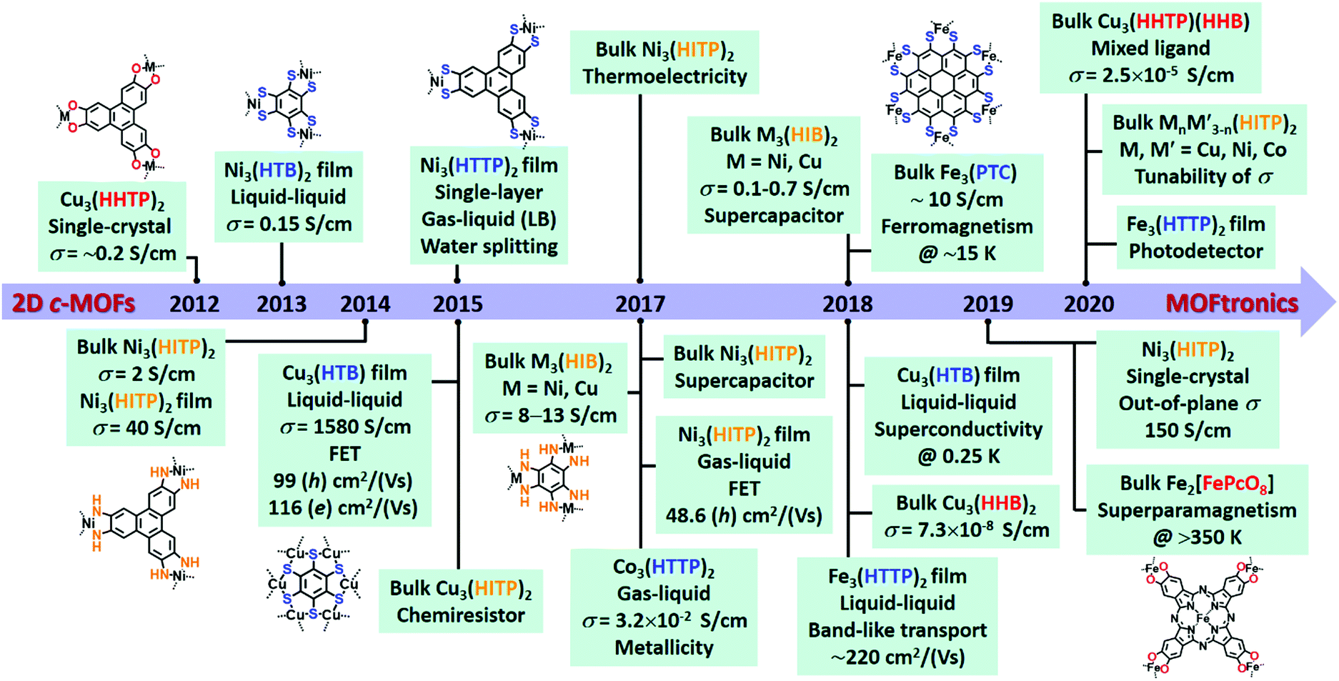 | ||
| Fig. 1 Timeline in the development of 2D c-MOFs from synthesis to MOFtronics. The ligands containing –OH, –NH2, and –SH are marked in red, orange, and blue colour, respectively. The Cu3(HHTP)(HHB) 2D c-MOF is also denoted as Cu3(HHTP)(THQ) (THQ = tetraoxyquinone in 2D c-MOFs). For 2D c-MOFs, HHTP represents 2,3,6,7,10,11-hexaoxytriphenylene instead of 2,3,6,7,10,11-hexahydroxytriphenylene for the monomer. | ||
This review article covers the chemistry and charge transport of 2D c-MOFs by consideration of structural diversity and structure–electronic property relationship based on the influence of molecular design (type and geometry of ligand, metal) and material structure (redox-activity in linkage, layer stacking and arrangement) on intrinsic charge transport properties. An overview of the synthetic methodologies including hydro-/solvothermal methods and wet-interface-assisted strategies is further offered. Next, device fabrications and the applications of 2D c-MOFs for MOFtronics are presented covering (opto)electronics (e.g. field-effect transistors, superconductors, chemiresistors, photodetectors), spintronics, thermoelectrics, and energy storage devices with the discussion of their achievements and existing challenges. Critical directions for future research are proposed towards MOFtronics within the community.
2. Chemical methodologies of 2D c-MOFs
After the first 2D c-MOF reported by Yaghi group in 2012,19 various ortho-substituted benzene- and triphenylene (TP)-based building blocks have been developed/employed for the formation of 2D c-MOFs, such as 1,2,3,4,5,6-hexahydroxybenzene (HHB),39 1,2,3,4,5,6-hexaaminobenzene (HAB),40 1,2,3,4,5,6-benzenehexathiol (BHT, also denoted asHTB),41 1,2,3,4,5,6-benzenehexaselenol (HSeB),42 2,3,6,7,10,11-hexahydroxytriphenylene (HHTP),19 2,3,6,7,10,11-hexaaminotriphenylene (HATP),43,44 2,3,6,7,10,11-triphenylenehexathiol (THT, also denoted as HTTP),45 2,3,6,7,10,11-triphenylenehexaselenol (HSeTP).46 Larger conjugated monomers have been developed and explored for the synthesis of 2D c-MOFs as well (Fig. 2), e.g. 2,3,8,9,14,15-hexahydroxytrinaphthylene (HHTN),47 2,3,7,8,12,13-hexahydroxytruxene (HHTX),48 metal(II) 2,3,8,9,14,16-hexaaminohexaazatrinaphthylene (HAHATNM′3, M′ = Cu, Ni, Co),49 1,2,3,4,5,6,7,8,9,10,11,12-perthiolated coronene (PTC),32 metal(II) 2,3,9,10,16,17,23,24-octahydroxyphthalocyanine (M′Pc(OH)8, M′ = H2, Cu, Fe, Ni, Zn),33,50–53 metal(II) 2,3,9,10,16,17,23,24-octaaminophthalocyanine (M′Pc(NH2)8, M′ = Cu, Ni),54,55 metal(II) 3,4,12,13,21,22,30,31-octahydroxynaphthalocyanine (M′NPc(OH)8, M′ = Ni).51 Besides, a non-planar conjugated ligand, 2,3,6,7,10,11,14,15-octahydroxydibenzo[g,p]chrysene (DBC(OH)8),56 was included into the 2D c-MOF family recently.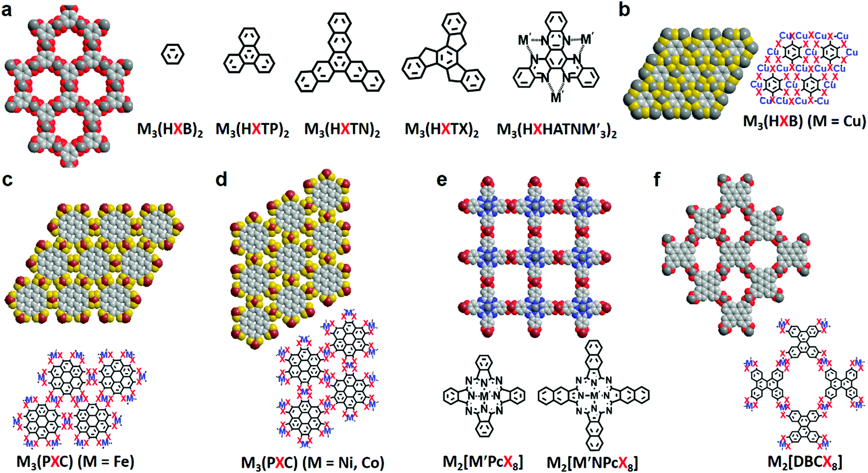 | ||
| Fig. 2 Structure of various 2D c-MOFs. (a) 2D c-MOFs with honeycomb lattice. M3(HXB)2, M3(HXTP)2, M3(HXTN)2, M3(HXTX)2, M3(HXHATNM′3)2. (b–d) Non-porous 2D c-MOFs. M3(HXB) (M = Cu; X = S, Se) and M3(PXC) (M = Fe, Ni, Cu; X = S). (e) 2D c-MOFs with square lattice. M2[M′PcX8] (M = Fe, Co, Ni, Cu, Zn; M′ = Fe, Ni, Cu, Zn; X = O, NH) and M2[M′NPcX8] (M = Ni, Cu; M′ = Ni; X = O). (f) Non-planar 2D c-MOF. M2[DBCX8] (M = Cu; X = O). | ||
In fact, the ligands in most of the thus-far constructed 2D c-MOFs are partially oxidized to form charge-neutral frameworks, instead of the generally displayed structures which correspond to negatively charged linkages (e.g. Cu3(HHTP)2, Fig. 10 in Section 4.1).19,23,25,40,55–58 Meanwhile, negatively charged 2D c-MOFs are also present in this emerging field, such as Cu3(HHB)2 (Section 3.4).39,59 Among the reported 2D c-MOFs, three types of linkages containing chelating functional groups were usually adopted: metal-bis(dioxolene) (abbreviated as MO4), metal-bis(diimine) (MN4, also termed as metal-bis(iminobenzosemiquinoid)), and metal-bis(dithiolene) (MS4) complexes (M = Fe, Co, Ni, Cu, Zn, Pd, or Pt). Due to the presence of both neutral and charged MO4-linked networks, the term of dioxolene instead of the normally applied semiquinoid is likely more reasonable.25,60 In addition, metal-diimine-dithiolene (MN2S2) mixed linkage and metal-bis(diselenolene) (MSe4) linkage were also investigated in few reports.42,46,61–63 Among these various linkages, Cu and Ni represented the majority of metal nodes, while Fe and Co were widely utilized for the construction of MS4. By contrast, the utilization of Zn, Pd, and Pt remains very limited.53,64–67
Due to the increasing ligand library and the diverse compositions, a uniform description shall be helpful for the development of 2D c-MOF families. Based on the mostly accepted style, we label the benzene- and triphenylene-based 2D c-MOFs as Mn(HXL)m (Fig. 2a), in which M and L represent the type of metal node and abbreviation of the building block (B for benzene, TP for triphenylene) respectively for a smallest repeating unit in their chemical structures, while H and X correspond to six substituent X in each ligand (X = O, NH, S, and Se). This can be also applied to trinaphthylene (TN)-, truxene (TX)- and hexaazatrinaphthylene (HATN)-based systems as Mn(HXTN)m, Mn(HXTX)m, and Mn(HXHATNM′3)m (Fig. 2a). Among all these systems, n and m—the number of metal nodes and ligands—are confirmed to be 3 and 2 respectively in general, except for rare instances including Ni9(HHTP)4, Co9(HHTP)4 (Fig. 10c),19 Cu3(HTB), and Cu3(HSeB) (n = 3, m = 1, Fig. 2b).31,42,68 For a non-porous 2D c-MOF based on the fully substituted coronene,32 M3(PXC) is adopted (Fig. 2c and d), in which P and C represent full substitution in the ligand, and the abbreviation of coronene, respectively. However, the octa-substituted metallophthalocyanine (M′Pc) and dibenzo[g,p]chrysene (DBC) are complicated systems. Instead of a scientific abbreviation for the ligands, the visualized one (M′PcX8 for M′Pc,33,50–52,54,55 DBCX8 for DBC56) is applied, thus leading to M2[M′PcX8] (Fig. 2e) and M2[DBCX8] (Fig. 2f) 2D c-MOFs, respectively. This address is also applicable to the larger metallonaphthalocyanine (M′NPc) system (Fig. 2e).51 Notably, three-dimensional (3D) MOFs without layer-stacked structures could be also constructed based on planar ligands (e.g. HHTP, CoPc(OH)8) through metal-catecholate linkages.69–72 Therefore, the structure of 2D c-MOFs highly depends on the employed ligands, metal centers and synthetic conditions.73
3. Chemical structure and electronic property relationship in 2D c-MOFs
Conductivity (σ) represents the transport of carriers of electrons (e) and holes (h), which can be quantified with mobility (μ) and density (n): σ = e(neμe + nhμh). Free charge carriers in 2D c-MOFs can be generated through thermal/photo-population or charge carrier injection through redox reactions.23,74,75 In this context, both the metal nodes (Frontier orbitals) and the ligands can serve as the sources. The potential charge transport pathways in 2D c-MOFs were ascribed as: through-bond, extended conjugation, through-space, and hopping.25 Particularly, through-bond or extended conjugation pathways in the 2D plane and through-space channel (strong π–π stacking and weak metal–metal interactions) dominate the intrinsic conductivity of 2D c-MOFs, while hopping stems from the charge carrier migration through grain boundaries, defects, etc. Many inspiring review articles have provided in-depth understanding on the above transport mechanism as well as the description of current characterization methods toward conductivity measurement, such as two-probe and four-probe (linear four-probe or van der Pauw) configurations.17,20,22–25,60,76Table 1 lists the currently reported 2D c-MOFs and the related studies on charge transport, including the sample form, characterization method, conductivity and mobility. Hereby, we would like to discuss the influence of molecular design (type and geometry of ligand, metal) and material structure (redox-activity in linkage, layer stacking and arrangement) as well as crystallinity on the charge transport properties for thus-far reported materials.| 2D c-MOF | Building block | Type | Method | σ (S cm−1) | μ (cm2 V−1 s−1) | Ref. |
|---|---|---|---|---|---|---|
| a Electrical conductivity at room temperature. b Van der Pauw. c Nanosheets. d Hall effect. e Device based on single-crystal. f a = 2.47, b = 0.53. g Field-effect transistor. h Reduced 2D c-MOF with charge state of −1. i Oxidized 2D c-MOF with charge state of 0. | ||||||
| Metal-bis(dioxolene) linked 2D c-MOFs | ||||||
| Cu3(HHB)2 | B | Pellet | vdPb | 7.8 × 10⁻⁸ | 39 | |
| Pellet | — | 2.2 × 10⁻⁹ | 87 | |||
| Pelletc | vdP | 1.5 × 10⁻⁷ | 2.4 (Hall, hd) | 88 | ||
| Cu3(HHTP)2 | TP | Pellet | 2-Probe | 1.0 × 10⁻² | 89 | |
| Pellet | 2-Probe | 3.0 × 10⁻³ | 90 | |||
| Pellet | 2-Probe | 2.0 × 10⁻³ | 91 | |||
| Pellet | 4-Probe | 2.0 × 10⁻² | 92 | |||
| Pellet | vdP | 4.5 × 10⁻² | 93 | |||
| Pellet | vdP | 2.7 × 10⁻² | 94 | |||
| Pellet | — | 0.09-0.1 | 95 | |||
| Film | 2-Probe | 2.0 × 10⁻² | 96 | |||
| Film | 4-Probe | 0.29 | 97 | |||
| Film | — | 10−4 | 98 | |||
| Nanorode | 4-Probe | 0.21 | 19 | |||
| Nanorode | 4-Probe | 1.5 | 95 | |||
| Nanoflakee | 2-Probe | 0.5 | 95 | |||
| Ni9(HHTP)4 | TP | Pellet | 2-Probe | 6.0 × 10⁻³ | 99 | |
| Pellet | 4-Probe | 1.0 × 10⁻² | 100 | |||
| Pellet | 4-Probe | 0.1 | 92 | |||
| Pellet | 4-Probe | 0.26 | 101 | |||
| Pellet | vdP | 6.8 × 10⁻³ | 94 | |||
| Film | vdP | 1.1 × 10⁻³ | 94 | |||
| Hybrid | 2-Probe | 1.6 × 10⁻⁴ | 102 | |||
| Co9(HHTP)4 | TP | Pellet | 2-Probe | 2.0 × 10⁻³ | 99 | |
| Pellet | 4-Probe | 2.7 × 10⁻⁶ | 92 | |||
| Pellet | vdP | 3.2 × 10⁻² | 94 | |||
| Film | vdP | 3.3 × 10⁻³ | 94 | |||
| Cu3(HHTP)(HHB) | TP/B | Pellet | 2-Probe | 2.5 × 10⁻⁵ | 59 | |
| Cu3(HHTN)2 | TN | Pellet | 2-Probe | 9.6 × 10⁻¹⁰ | 47 | |
| Cu3(HHTX)2 | TX | Pellet | 2-Probe | 8.3 × 10⁻⁴ | 48 | |
| Cu2[DBCO8] | DBC | Pellet | — | 1 × 10⁻² | 56 | |
| Cu2[CuPcO8] | Pc | Pellet | 2-Probe | 9.4 × 10⁻⁸ | 50 | |
| Pellet | 2-Probe | 1.6 × 10⁻⁶ | 50 | |||
| Cu2[NiPcO8] | Pc | Pellet | 4-Probe | 1.4 × 10⁻² | 51 | |
| Ni2[NiPcO8] | Pc | Pellet | 4-Probe | 7.2 × 10⁻⁴ | 51 | |
| Fe2[FePcO8] | Pc | Pellet | vdP | ∼1 × 10⁻⁵ | ∼0.1 (Hall, h) | 33 |
| Pellet | — | — | 15 (TRTS) | 33 | ||
| Cu2[NiNPcO8] | NPc | Pellet | 4-Probe | 3.1 × 10⁻² | 51 | |
| Ni2[NiNPcO8] | NPc | Pellet | 4-Probe | 1.8 × 10⁻² | 51 | |
| Metal-bis(diimine) linked 2D c-MOFs | ||||||
| Cu3(HIB)2 | B | Pellet | 4-Probe | 0.1 | 38 | |
| Pellet | vdP | 13 | 40 | |||
| Ni3(HIB)2 | B | Pellet | 4-Probe | 0.7 | 38 | |
| Pellet | vdP | 8 | 40 | |||
| Co3(HIB)2 | B | Pellet | 4-Probe | 0.1–1.57 | 35 | |
| Cu3(HITP)2 | TP | Pellet | 2-Probe | 0.2 | 28 | |
| Pellet | 4-Probe | 0.75 | 58 | |||
| Ni3(HITP)2 | TP | Pellet | 2-Probe | 2 | 57 | |
| Pellet | 4-Probe | 39 | 101 | |||
| Pellet | 4-Probe | 1.896 | 103 | |||
| Pellet | — | 0.5 | 104 | |||
| Pellet | vdP | 50 | 37 | |||
| Pellet | 4-Probe | 55.4 | 58 | |||
| Pellet | vdP | 58.8 | 105 | |||
| Film | — | 37.2 | 104 | |||
| Film | 2-Probe | 8.5 × 10⁻³ | 106 | |||
| Film | 2-Probe | 0.23 | 106 | |||
| Film | vdP | 40 | 57 | |||
| Hybrid | 2-Probe | 2.6 × 10⁻³ | 102 | |||
| Nanorode | 4-Probe | 150 | 95 | |||
| Film | FET g | — | 48.6 (h) | 29 | ||
| Film | FET g | — | 45.4 (h) | 107 | ||
| Co3(HITP)2 | TP | Pellet | 4-Probe | 8 × 10⁻⁴ | 103 | |
| Pellet | 4-Probe | 0.024 | 58 | |||
| CoaCub(HITP)2f | TP | Pellet | 4-Probe | 5.8 × 10⁻³ | 58 | |
| Ni3(HXHATNNi3)2 | HATN | Pellet | 4-Probe | 2 | ||
| Ni2[NiPc(NH)8] | Pc | Film | 4-Probe | 0.2 | 54 | |
| Ni2[CuPc(NH)8] | Pc | Pelletc | vdP | ∼1 × 10⁻⁴ | 1.6 (Hall, h) | 55 |
| Metal-bis(dithiolene) linked 2D c-MOFs | ||||||
| Cu3(HTB) | B | Pellet | 4-Probe | 48–280 | 108 | |
| Film | 4-Probe | 1580 | 31 | |||
| Film | FET g | — | 116 (e), 99 (h) | 31 | ||
| Film | 4-Probe | 2500 | 68 | |||
| Ni3(HTB)2 | B | Pellet | 2-Probe | 0.15 | 74 | |
| Pellet | 2-Probe | 6.7 × 10⁻³ | 74 | |||
| Pellet | 2-Probe | 2.8 | 75 | |||
| Pellet | 2-Probe | 160 | 75 | |||
| Pd3(HTB)2 | B | Film | 4-Probe | 2.8 × 10⁻² | 65 | |
| Cu3(HTTP)2 | TP | Pellet | — | 2.4 × 10⁻⁸ | 109 | |
| Ni3(HTTP)2 | TP | Pellet | — | 3.6 × 10⁻⁴ | 109 | |
| Co3(HTTP)2 | TP | Pellet | — | 2.4 × 10⁻⁹ | 109 | |
| Pellet | vdP | 1.4 × 10⁻³ | 79 | |||
| Film | vdP | 3.2 × 10⁻² | 79 | |||
| Fe3(HTTP)2 | TP | Film | vdP | 3.4 × 10⁻² | 229 (Hall, h) | 78 |
| Film | — | — | 211 (TRTS) | 78 | ||
| Film | vdP | 0.2 | 80 | |||
| Pt3(HTTP)2 | TP | Pellet | 2-Probe | 3.9 × 10⁻⁶ | 64 | |
| Fe3(PTC) | C | Pellet | vdP | 10 | 32 | |
| Ni3(PTC) | C | Pellet | 4-Probe | 9 | 110 | |
| Co3(PTC) | C | Pellet | 4-Probe | 45 | 111 | |
| Metal-diimine-dithiolene linked 2D c-MOFs | ||||||
| Ni3(TITTB)2 | B | Pellet | vdP | 0.1 | 63 | |
| Pellet | vdP | 3 × 10⁻⁶ | 62 | |||
| Metal-bis(diselenolene) linked 2D c-MOFs | ||||||
| Cu3(HSeB) | B | Pellet | 4-Probe | 110 | 42 | |
| Co3(HSeTP)2 | TP | Pellet | 2-Probe | 10−6 | 46 | |
3.1 Effect of ligand type
The current ligands utilized for the construction of 2D c-MOFs have been mainly based on the planar conjugated building blocks with symmetrical functional groups of –OH, –NH2, and –SH. Varying the functional groups results in increased bond strength between metals and linkers from MO4 to MN4 to MS4,25 thus leading to the apparent enhancement of the in-plane charge transport along the 2D network. Density functional theory (DFT) calculations indicated that the linker substitution in MX4 (X = O, NH, and S) also affects the dynamic stability of the frameworks; Zn3(HTB) is more stable than Zn3(HSeB) whilst Zn3(HHB) is the most unstable one.77 In addition, energy matching of the d orbitals of different transition metals with the π-conjugated ligands generally generates the difference in π–d hybridization, hence tuning the delocalization of carriers in the 2D plane to a different extent (Section 3.3). Among these 2D c-MOFs, MO4-linked ones exhibited apparently inferior charge transport to the related 2D c-MOFs linked by the MN4 coordination complex. For instance, charge-neutral MO4-linked Cu3(HHTP)2 could display broad conductivity values in the range of 10−4 to 1 S cm−1 measured by 2-/4-probe measurement in their pellet form at room temperature. By contrast, the pellet samples of MN4-linked Cu3(HITP)2 could exhibit higher conductivity values in the range of 0.2–0.75 S cm−1. Regarding Pc-based M2[M′PcX8] 2D c-MOFs, the MN4-linked samples also showed superior conductivity than the MO4-linked ones. The MS4 complex presents the highest π–d hybridization among these linkages, and therefore thus-far reported MS4-linked 2D c-MOFs have been demonstrated to exhibit excellent conductivity and mobility. For example, the Ni3(HTB)2 film showed a conductivity of ∼160 S cm−1 and the non-porous Cu3(HTB) film could even exhibit a conductivity as high as ∼2500 S cm−1 (shown in Table 1). Besides the conductivity, another typical MS4-linked sample, Fe3(HTTP)2, was observed to present a notable band-like transport with record high charge mobility >200 cm2 V−1 s−1 amongst the reported 2D c-MOFs due to the high π–d conjugation.78 The Co3(HTTP)2 2D c-MOF was recorded to possess a negative temperature–resistivity relationship in the high temperature region and a positive trend at low temperature for semiconducting and metallic behavior, respectively.79,80 Recently, MSe4-linked bulk 2D c-MOFs have been developed and displayed lower conductivity (e.g. Cu3(HSeB): 110 S cm−1, Co3(HSeTP)2: 10−6 S cm−1) than those of MS4-linked bulk 2D c-MOFs (Table 1).42,46Varying the functional groups will also vary the coordination bond length between metal nodes and linkers in the MX4-linkages due to the difference of the atom radius of the O, N, S, and Se (Se > S > O > N), which plays also an important role in the charge transport and other physical properties. For instance, for some selected square-planar Ni-coordinated complexes (Fig. 3A–C), the bond lengths are 1.866, 1.822–1.826, and 2.132–2.170 Å for Ni–O, Ni–N, and Ni–S bonds, respectively.81–83 While for 2D c-MOFs, Ni3(HITP)2 and Ni3(HTTP)2, powder X-ray diffraction (PXRD) indicated prominent (100) peak (Cu-Kα radiation) with 2θ = 4.7° (1.88 nm) and 4.5° (1.96 nm) respectively, indicative of larger lattice constant of Ni3(HTTP)2 than Ni3(HITP)2 due to the presence of its longer Ni–S bond.29,45,57 A similar phenomenon was revealed by the DFT calculations: ∼0.1 nm smaller lattice constant of Mn3(HIB)2 than Mn3(HTB)2.84,85 In a monolayer of Mn3(HIB)2, the shorter distance between Mn2+ ions is expected to enhance the magnetic coupling; compared with MS4, N atoms in the MN4 linkage are more effective at mediating the magnetic couplings. As a result, the monolayer of Mn3(HIB)2 is predicted to possess a transition temperature for ferromagnetic coupling at ∼450 K, which considerably surpasses that of 212 K for a single-layer of Mn3(HTB)2.84 Nevertheless, it remains not sufficient to quantitatively compare the influence of the MX4-linkages on conductivity, due to the few examples and the heterogeneous sample morphologies, potential doping, as well as the lack of unique features of chemical composition and structural geometry for individual samples.
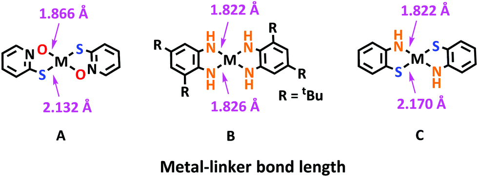 | ||
| Fig. 3 The bond length of metal-linkers (O, NH, S) in the MX4 linkage. Selected structures of A,75 B,74 and C76 refer to reported metal-complex small molecules. | ||
3.2 Effect of ligand geometry
Ligand geometry and symmetry are of key significance for the construction of regular frameworks of 2D c-MOFs. Currently, three types of networks have been developed for 2D c-MOFs, including hexagonal, square, and honeycomb lattices with polygons of triangles, squares, and hexagons, respectively (Fig. 4). For the construction of hexagonal, square, or honeycomb frameworks, symmetric ligands with C6 (e.g. PTC), C4 (e.g. M′PcX8), or C3 (e.g. HXTP) geometry respectively are required. Importantly, the resulting framework geometry is relevant to the electronic structure of the achieved 2D c-MOF. For example, the hexagonal and square geometries correlate with a structure, where only one type of vertex exists in each unit cell with six neighboring triangles or four neighboring squares (Fig. 4a and b, unit cells are marked red in the middle figures). DFT calculations indicated that only one type of band is presented in the band structures for both geometries.86 On the other hand, each unit cell contains two vertices in different environments in a honeycomb network (Fig. 4c). As a result, two bands appear in the energy band diagram forming the Dirac point.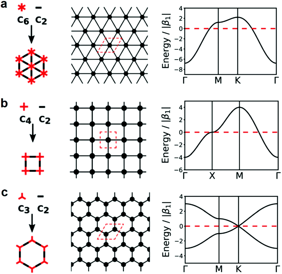 | ||
| Fig. 4 Topological diagrams of the networks and 2D representations with different geometries (unit cells are marked in red) as well as corresponding band structures. (a) Hexagonal. (b) Square. (c) Honeycomb. C2 monomer refers to metal ions here ref. 86. Copyright 2020, the Royal Society of Chemistry. | ||
Though a dual-porous kagome network (Fig. 5a, left) is not presented among thus-far reported 2D c-MOFs, the metal atoms in the honeycomb frameworks (e.g. M3(HXB)2, M3(HXTP)2) are arranged in the kagome lattice (Fig. 5a, middle), which exhibits a band structure including a Dirac point and a flat band above the Dirac bands (Fig. 5a, right).86 The framework with extended π-conjugation in a kagome lattice is predicted to exhibit nontrivial physical properties. For instance, first-principles calculations indicated that a single-layer of Ni3(HTB)2 possesses the typical kagome bands: a flat band above two Dirac bands (Fig. 5b and c). The local density of state of a semi-infinite Ni3(HTB)2 framework for spin-up and spin-down components indicated nontrivial topological edge states (Fig. 5d and e), indicative of the possible existence of an organic topological insulator.112 Besides, a monolayer of Ni3(HITP)2 (Fig. 8b) or Cu3(HITP)2 also exhibited Dirac bands near the Fermi level.113
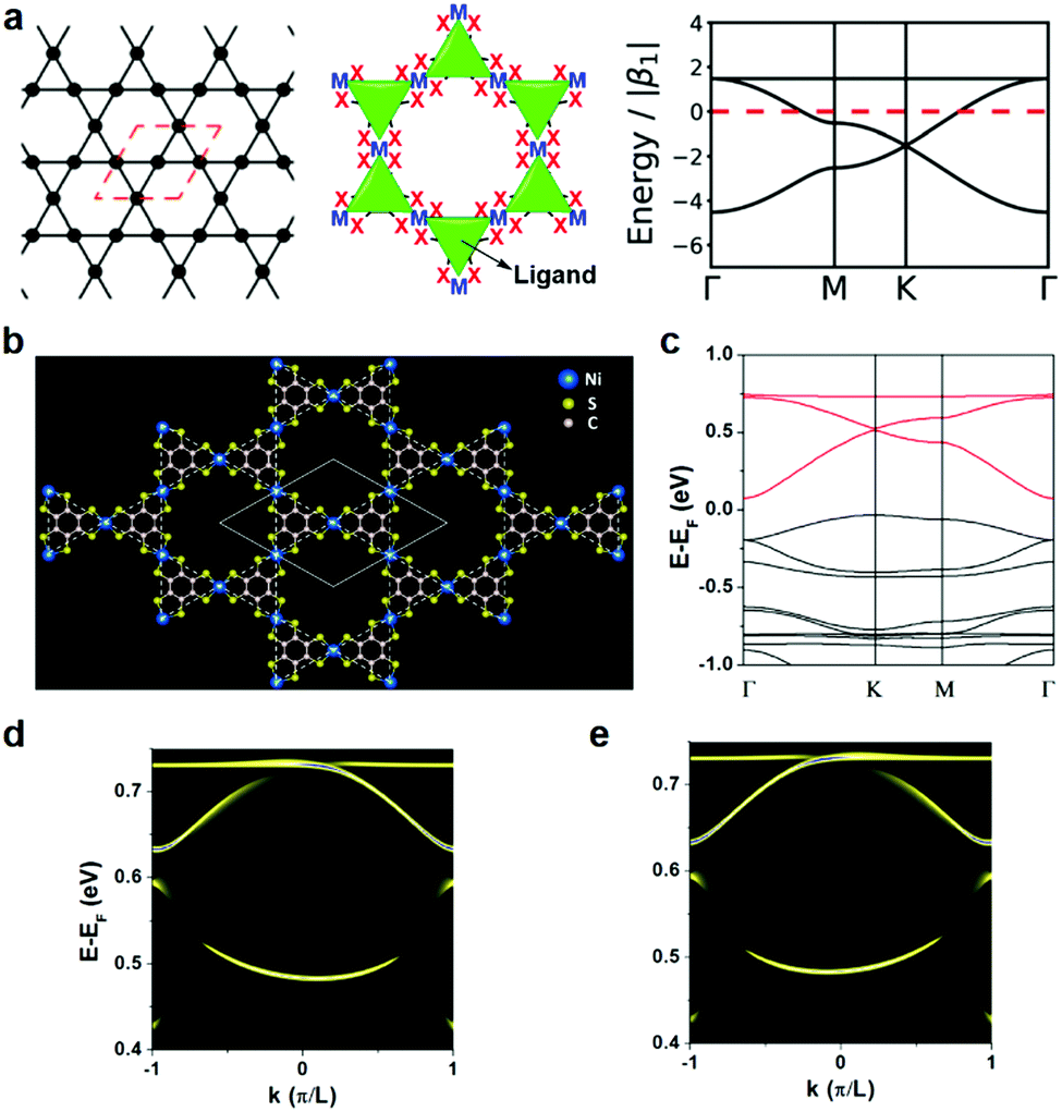 | ||
| Fig. 5 Kagome lattice in 2D c-MOFs. (a) Topological diagram of the kagome network (left), the kagome lattice of metal atoms in a honeycomb network (middle), and the band structure for a kagome network (right).86 Copyright 2020, the Royal Society of Chemistry. (b) Kagome lattice of the Ni3(HTB)2 monolayer. The dashed lines outline the kagome lattice. (c) The band structure of the Ni3(HTB)2 monolayer. (d and e) The semi-infinite edge states of the spin-up and spin-down components for the Ni3(HTB)2 monolayer, respectively. Reproduced with permission ref. 112. Copyright 2013, American Chemical Society. | ||
In addition to the type and geometry of the ligand, the ligand size (e.g. benzene, triphenylene, trinaphthylene), which correlates with diverse densities of building blocks and linkages as well as the π-conjugation degree in the network, is also an important parameter for the electronic structures. However, accompanied by other factors, such as the lattice, layer distance, porous density, etc., the influences of ligand size remain elusive. Besides, the control of π-conjugation degree in the building blocks (e.g. benzene, triphenylene, trinaphthylene, coronene, phthalocyanine) is expected to efficiently vary the conductivity and mobility of 2D c-MOFs in both in-plane and cross-plane directions. Nonetheless, because of the differences in the geometry and size of the ligand, a proper relationship between π-conjugation and conductivity has been so far elusive.
3.3 Effect of metals
The metal centers have been demonstrated to play an important role in the electronic properties of the 2D c-MOFs. It is already known that the conductive 3D MOFs with mixed valence Fe atoms (Fe2/3+) show superior electrical conductivity to the pure Fe2+-bridged ones.114–117 For instance, fractional reduction of Fe3+ atoms in Fe2(BDP)3 (BDP = 1,4-benzenedipyrazolate) to access mixed valence state of Fe2/3+ in the framework resulted in a nearly four orders of magnitude higher conductivity along a single crystallographic axis.115 For 2D c-MOF systems, many examples possess mixed valence as well, such as Fe2/3+, Co2/3+, and Cu1/2+.33,39,56,80,118 Nevertheless, the valence influence on the electronic properties has not been systematically investigated due to the lack of control on the metal valence. For the moment, we would assume a similar conclusion in 2D c-MOFs compared with conductive 3D MOFs.On the other hand, the metal type also plays an important role in the charge transport performance of 2D c-MOFs.58,119 For instance, first-principles calculations indicated that the band gaps of M3(HTB) (M = Mg, Ca, Zn, Cd, Ge, and Sn) ranged from 1.7 to 3.2 eV.120 Besides, the π–d hybridization between d (metal) and π (HTB) bands can considerably delocalize the wave function of band edge states and is of importance in determining their hole effective masses. More specifically, as the π–d coupling increases from the elements of group IIA (Mg, Ca) to IVA (Ge, Sn) to IIB (Zn, Cd), the hole effective masses decrease significantly. While for electron transport, from group IIB (Zn, Cd) to IIA (Mg, Ca) to IVA (Ge, Sn), the electron effective masses increase.120 Nonetheless, these 2D c-MOFs have so-far not been constructed in the laboratory. In addition, great efforts from DFT calculations have been also devoted to the well-known M3(HITP)2 (M = Ni, Cu) 2D c-MOFs regarding the metal substitution. The substitution from Ni to Cu in this system will change both the geometries and the electronic band structures (Fig. 6a). The Ni atoms in Ni3(HITP)2 adopt the dsp2 hybridization in a square-planar geometry, thus forming a planar 2D framework.113 Nevertheless, for Cu3(HITP)2, the Cu atoms adopt the sp3 hybridization leading to a distorted network in a specific square-grid coordination geometry. In addition, a single-layer of Cu3(HITP)2 is metallic whilst the monolayer of Ni3(HITP)2 is an indirect semiconductor.113
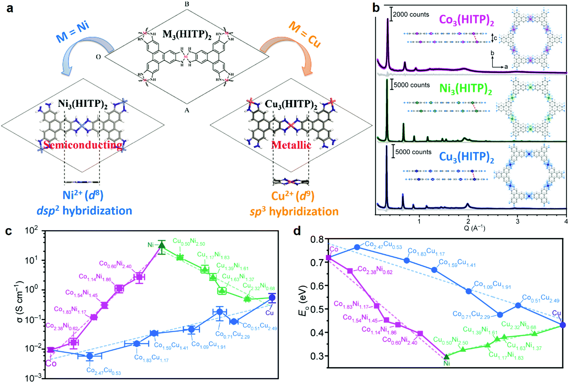 | ||
| Fig. 6 Metal substitution in 2D c-MOFs. (a) Illustration of the geometry of M3(HITP)2 (M = Ni, Cu) by substituting Ni (left) with Cu (right).113 Copyright 2015, the PCCP Owner Societies. (b) Synchrotron X-ray diffraction patterns and Pawley refinements for M3(HITP)2. The insets show the bilayer of M3(HITP)2 with reference to the interlayer displacement. (c and d) Electrical conductivity and optical bandgap of MnM′3−n(HITP)2, respectively. Dashed lines refer to linear fitting. Reproduced with permission ref. 58. Copyright 2020, American Chemical Society. | ||
Experimentally, varying the metal center in the charge-neutral M3(HITP)2 2D c-MOF system could readily change the layer distance, which was determined as 3.30, 3.16, and 3.29 Å for Ni3(HITP)2, Cu3(HITP)2 and Co3(HITP)2, respectively (Fig. 6b).58 The layer distance refers to the strength of π–π stacking interactions, thereby enabling to define the electronic structure in the cross-plane direction (Section 3.5). According the PXRD analysis, the substitution of the metal center is also relevant to the interlayer displacement, which was recorded as 1.56, 0.86, and 1.39 Å respectively for the above 2D c-MOFs. Unsurprisingly, conductivities of these 2D c-MOF samples differed greatly, which were determined as 55.4, 0.75, and 0.024 S cm−1, respectively. In this work, Dincă and co-workers further demonstrated a series of binary alloys of MnM′3−n(HITP)2 consisting of two metal species (Co/Cu, Co/Ni, or Cu/Ni) within one network.58 Continuous shifts of the interlayer distance and displacement as well as conductivity were determined with an increasing amount of one metal. For instance, increasing the amount of Ni in the ConNi3−n(HITP)2 system shifts the values of layer distance and displacement in such a way as to enhance the π–π interactions, which results in a continuous increment of conductivity over 3 orders of magnitude from 0.024 to 55.4 S cm−1 (Fig. 6c) and a continuously tuned bandgap over 0.4 eV in fine-scale (Fig. 6d). While for the fully substituted coronene (PTC), the metal substitution from Fe to Ni/Cu results in not only changes in the conductivity but also in the variation of the chemical structures of 2D c-MOFs (Fig. 2c and d).32,110,111 In addition, the metal atoms play also an important role in the magnetic properties of 2D c-MOFs. In particular, due to the unique spin properties of Fe and the strong π–d hybridization between the d/p orbitals in the FeX4 complex, the resultant 2D c-MOFs exhibit nontrivial ferromagnetism (Section 6.3).32,33
3.4 Effect of redox-activity in linkage
Here, the redox activity majorly refers to the charge state of the linkages. Each linkage is able to undergo a two-electron transfer through redox reactions (Fig. 7), which corresponds to diverse charge state of the linkage as 0 (existence of monoradical), −1 (presence of counter cation), and 1 (presence of counter anion). Among the reported 2D c-MOFs, the ligands are generally partially oxidized providing free radicals as charge carriers (charge-neutral framework with a charge state of 0), which correlates with the density (n) of charge carriers in the frameworks.19,36,51,56,65,73–75 For example, Cu3(HHB)2 possesses a network with denser distributed ligands and metals as well as smaller layer distance (∼3 Å)39 compared with Cu3(HHTP)2 (∼3.3 Å);95 the former one was expected to display higher conductivity due to the stronger cross-plane π–π interactions (Section 3.5). However, conductivity experiments indicated inferior values in the range of (0.22–15) × 10−8 S cm−1 for Cu3(HHB)2, making it like an insulator. The huge difference would be attributed to the localized charge carriers due to the absence of free radicals with respect to a charge state of −1. While for Ni3(HTB)2, X-ray photoelectron spectroscopy (XPS) analysis revealed mixed charge states of 0 and −1 (ratio of 26![[thin space (1/6-em)]](https://www.rsc.org/images/entities/char_2009.gif) :74, corresponding to an average charge state of −3/4) in the nickel-bis(dithiolene) linkages for the as-synthesized sample (conductivity in the range of 0.15–2.8 S cm−1), indicative of the existence of few free radicals. It was demonstrated that additionally generated radicals upon oxidation offer abundant free carriers, thereby leading to enhanced conductivity values.74,75 For instance, the amount of radicals in Ni3(HTB)2 was further increased through oxidation reactions (charge state of 0), leading to significantly advanced conductivity up to 160 S cm−1. By comparison, the reduction reaction on the as-synthesized Ni3(HTB)2 led to a decreased conductivity of 6.7 × 10⁻³ S cm−1, which can be ascribed to the disappearance of those few radicals after chemical reduction (charge state of −1).
:74, corresponding to an average charge state of −3/4) in the nickel-bis(dithiolene) linkages for the as-synthesized sample (conductivity in the range of 0.15–2.8 S cm−1), indicative of the existence of few free radicals. It was demonstrated that additionally generated radicals upon oxidation offer abundant free carriers, thereby leading to enhanced conductivity values.74,75 For instance, the amount of radicals in Ni3(HTB)2 was further increased through oxidation reactions (charge state of 0), leading to significantly advanced conductivity up to 160 S cm−1. By comparison, the reduction reaction on the as-synthesized Ni3(HTB)2 led to a decreased conductivity of 6.7 × 10⁻³ S cm−1, which can be ascribed to the disappearance of those few radicals after chemical reduction (charge state of −1).
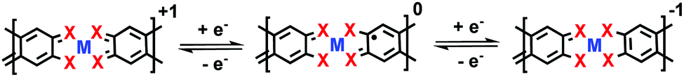 | ||
| Fig. 7 Redox activity of the linkage of 2D c-MOFs through electron transfer. | ||
3.5 Effect of layer stacking and arrangement
As is seen in 2D c-MOFs, linking the ortho-substituted conjugated ligands by square-planar metal coordination complexes yields an extended π-conjugated network, thus enhancing the delocalization of charge carriers within the 2D plane. The in-plane charge carrier migration was considered as the dominant pathway of the intrinsic charge transport in 2D c-MOFs. Nevertheless, in recent studies, DFT calculations and charge transport characterization based on single-crystals revealed the significance of the through-space pathway in the electronic properties. As mentioned in Section 3.3, a single-layer of Ni3(HITP)2 is predicted to be a semiconductor (bandgap of 0.13 eV) (Fig. 8a and b). The increased dimensionality from a monolayer to layer-stacked Ni3(HITP)2 leads to a significant change from semiconducting to metallic in the electronic band structure (Fig. 8c), which can be attributed to the strong π–π (d = 3.3 Å) and weak Ni–Ni (d = 3.809 Å) interactions in the direction perpendicular to the Ni3(HITP)2 layers.113 Very recently, the Dincă group characterized the out-of-plane conductivity of Ni3(HITP)2 up to 150 S cm−1 and demonstrated that interlayer π–π interactions indeed considerably contribute to the conductivity in layer-stacked 2D c-MOFs based on single-crystalline samples and related devices.95 Thus, it raised up an open question whether high-performance electrically conductive MOFs necessarily require the incorporation of in-plane conjugated structures. Another work from the same group reported layered lanthanide-HHTP MOFs with metal centers located in between the linker layers.121 The lanthanide-HHTP MOFs do not possess in-plane π–d conjugation but nevertheless display high electrical conductivity (up to 0.05 S cm−1).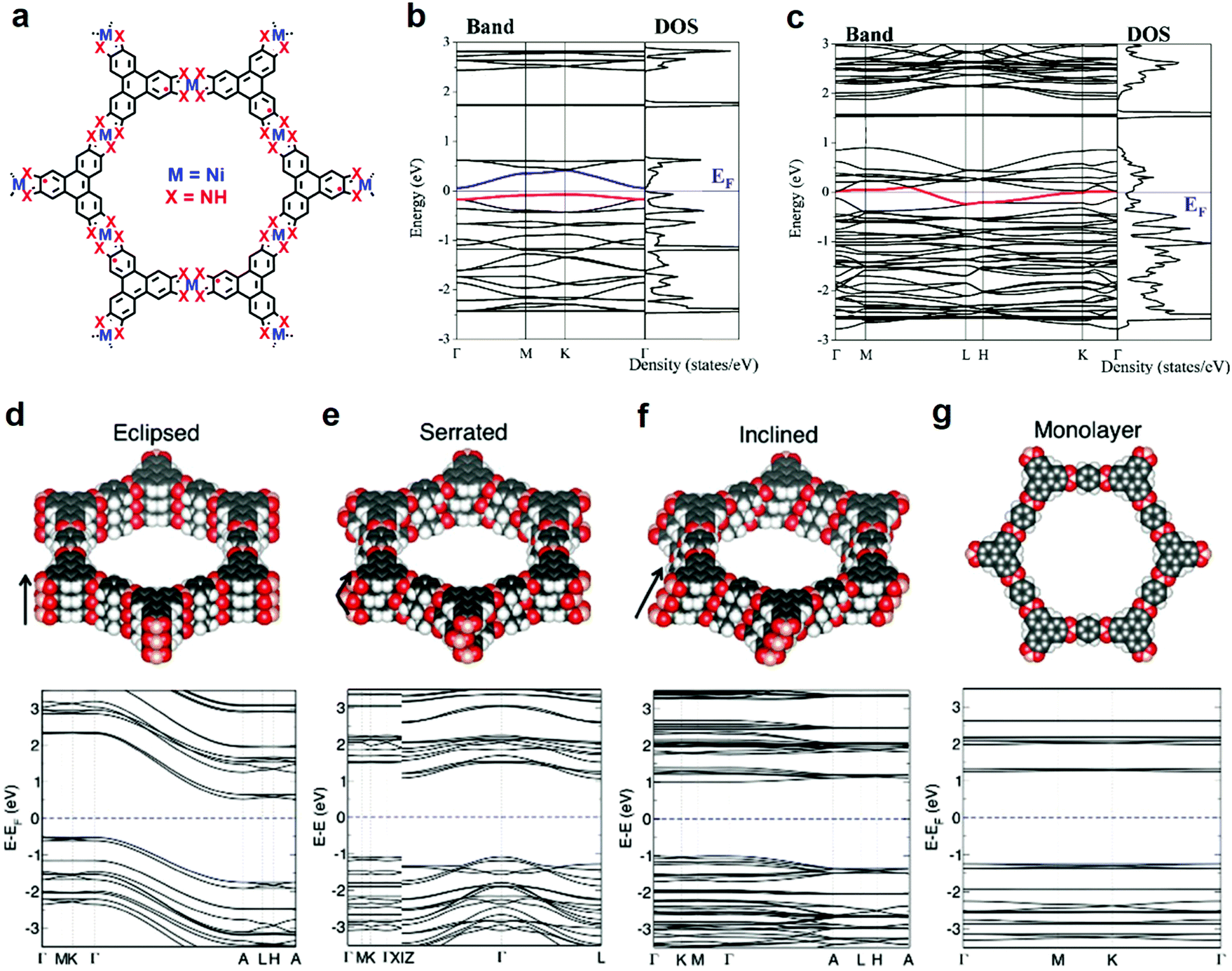 | ||
| Fig. 8 Electronic band structure with respect to layer stacking and arrangement. (a–c) Band structure for monolayer (b) and layer-stacked (c) Ni3(HITP)2.113 Copyright 2015, the PCCP Owner Societies. (d–f) AA-eclipsed, AA-serrated, and AA-inclined stacking of COF-5 as well as related band structures shown at the bottom. (g) Monolayer and related band structures of COF-5.129 Copyright 2020, Wiley-VCH. | ||
Rational tuning the interlayer spacing and modification of layer arrangement can induce significant changes in the electronic band structures as well as conductivities. Great efforts from DFT calculations have been devoted to the calculation of band structures and electrical properties for 2D c-MOFs.31–33,40,78–80,112,113,122–127 Combining experimental and computational analysis, the reported 2D c-MOFs preferred to stack in an AA-eclipsed (AAAA) symmetry (Fig. 8d), rather than the staggered AB (ABAB) mode.46,48,50,51,54 Taking carefully in the AA symmetry, the AA-serrated (AA′AA′) stacking (Fig. 8e), so called “slipped-parallel AB stacking” with slightly slipped arrangement in every two layers,19,28,32,33,36,39,40,42,52,53,57,59,68,96,97,99 and AA-inclined (AA′A′′A′′′, that is, the layers are continuously shifted in one direction) stacking (Fig. 8f)78 were suggested to be energetically more favored than the AA-eclipsed one in these highly conjugated systems. The stacking—refers to the arrangement of layers—affects the pore geometries128 and the electronic properties129 of 2D framework materials. Taking a representative 2D covalent organic framework (COF), COF-5,130 as an example, the band structure of a single-layer shows flat conduction and valence bands as well as typical signature of the kagome lattice68,112,113 along the Γ–K–M–Γ path (in-plane), while stacking the layers with different arrangements varies not only the out-of-plane charge transport, but also the in-plane one (Fig. 8d–g, bottom).129 The AA-eclipsed stacked COF-5 retains almost unchanged band structures with preserved signature of the kagome lattice in the in-plane direction (for details see ref. 129), while interlayer interactions induce strong cross-plane band dispersion hence narrowing the band gap from ∼2.5 (monolayer) to 1.3 eV. However, the AA-serrated and AA-inclined stacking modes strongly alter the in-plane electronic structure, leading to the absence of the kagome characteristic (for details see ref. 121). Compared with the eclipsed layer arrangement, both the serrated and inclined cases exhibit smaller out-of-plane dispersion due to the weaker π–π interactions, which corresponds to a larger band gap of 2.2 eV for both cases. In another instance, Fe3(HTTP)2 2D c-MOF, the band gap of a monolayer was calculated as 0.3 eV; it opens up to 0.35 and 0.65 eV for the AA-inclined and AA-eclipsed arrangements, respectively.78 Furthermore, the obtained effective mass (m*) values for AA-inclined stacking (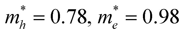 ) and AA-eclipsed stacking (
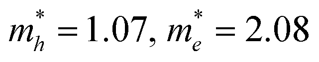 ) differ significantly from those for a monolayer (
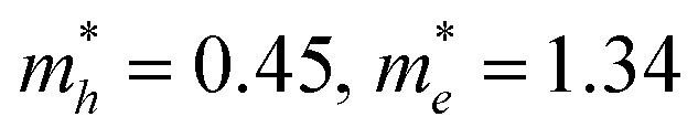 ) of Fe3(HTTP)2. Therefore, to evaluate the band diagrams in the absence of high structural resolution, several potential stacking sequences including not merely AA-eclipsed and AB arrangements merit thorough consideration.
In addition to the foregoing points, high crystallinity or even single-crystal not only offers a high-quality sample but also allows precise structural analysis,71,131–133 thus ensuring the establishment of a reliable structure–property relationship. The polycrystalline Cu3(HITP)2 possessed a mixed valence of Cu1/2+ in the as-synthesized sample.28 However, all Cu atoms presented to be Cu2+ in the single-crystalline sample hence ruling out the contribution of mixed valences to conductivity.58 The mixed valence of Cu1/2+ could be ascribed to the presence of defects or amorphous regions in the less crystalline Cu3(HITP)2 sample. Furthermore, the conductivity value of the compressed pellet of Cu3(HITP)2 single-crystals increased from 0.2 S cm−1 for the polycrystalline Cu3(HITP)2 to 0.75 S cm−1. In another example, the highly crystalline Cu3(HTB) film exhibits a conductivity reaching 2500 S cm−1,68 while the conductivity of the one with low crystallinity (according to the X-ray diffraction and transmission electron microscopy analysis) was merely determined to be 1580 S cm−1.31,134 In addition, the synthesized M3(HIB)2 (M = Cu, Ni, Co) films were reported as an electrical insulator in the early work from Lahiri et al.,135 which is likely attributed to the low crystallinity in these samples. By comparison, their intrinsic metallicity was confirmed in the highly crystalline bulk samples (M = Cu, Ni) by ultraviolet-photoelectron spectroscopy. Conductivity measurements on the pellets revealed characteristic values of 8 and 13 S cm−1 for Ni3(HIB)2 and Cu3(HIB)2, respectively.40 The polycrystalline Ni3(HITP)2 2D c-MOF displayed temperature-dependence suggesting a semiconducting behavior and a conductivity up to ∼60 S cm−1,57 while single-crystalline Ni3(HITP)2 nanorod sample presented metallicity with a higher conductivity of ∼150 S cm−1 through the cross-plane direction.95 Thus, single-crystalline devices that can minimize the influence of grain boundary and disorder on the charge transport are urgently required for characterizing 2D c-MOFs.29,57 Besides conductivity, few reports attempted to probe the type of carriers and charge mobility as well as density for 2D c-MOFs in the direct current (DC) limits including field-effect transistors and Hall effect measurements, as well as in the alternating current (AC) limits such as contact-free time-resolved terahertz spectroscopy (TRTS) and flash photolysis-time-resolved microwave conductivity.33 An in-depth understanding of the mechanism underlying the conductivity and the establishment of a reliable structure–property relationship through combining multi-scaled physical characterization methods merit further exploration.
4. Synthetic methodologies of 2D c-MOFs
Currently, various synthetic methodologies have been applied to develop 2D c-MOFs as bulk or film samples. Hydro-/solvothermal syntheses represent a representative strategy (Fig. 9) that allows diversity in the reaction conditions including the solvent, temperature, volume and pressure, and offers advantages in scalable and high-yield synthesis. They also provide the possibility to achieve moderate-sized (1–10 μm) single-crystals.19,95 Nevertheless, the obtained bulk materials generally comprise nanocrystals smaller than 100 nanometers (nm), associating with difficulties in sample processing, device fabrication, and charge transport characterization. Recently, the wet-interface-assisted synthesis21,136–142 shows promise in preparing crystalline, large-area, free-standing 2D c-MOF thin films. These films ensure facile device integration (notably for electronic devices) and sufficient charge transport29,31,36,41,57,68,74,75,78–80,96,97,143 that holds potential to realize the practical applications of these materials for MOFtronics. Nonetheless, the universality of this interfacial strategy towards large π-conjugated systems, the further improvement of the crystallinity and the mechanical strength of the film as well as the control of the film thickness are still synthetic challenges. In the following sections, we will introduce these synthetic methodologies toward 2D c-MOFs and discuss the current achievements and challenges.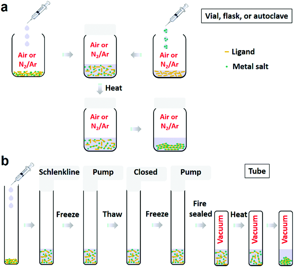 | ||
| Fig. 9 Schematic illustration of various hydro-/solvothermal syntheses methods. (a) Under ambient or inert atmosphere. (b) Under vacuum. | ||
4.1 Bulk 2D c-MOFs through hydro-/solvothermal syntheses
In 2012, Hmadeh et al. reported a series of TP-based MO4-linked 2D c-MOFs by heating an aqueous solution of HHTP and metal(II) acetate (M = Cu, Ni, Co) at 85 °C for 24 hours (Fig. 9a and 10a).19 Scanning electron microscopy (SEM) revealed uniform morphology of the obtained samples as nanorods with length less than 10 μm and diameter of ∼100 nm (Fig. 10e). Their crystal structures were resolved by single-crystal X-ray diffraction, PXRD, and high-resolution transmission electron microscopy (HR-TEM). These 2D c-MOFs possess two different structures: (1) Cu3(HHTP)2 (Fig. 10b) with a layered honeycomb network and (2) M9(HHTP)4 (discounting water molecules, M = Co, Ni) (Fig. 10c) comprising alternatively layered honeycomb frameworks of M3(HHTP)2(H2O)6 (each M2+ is coordinated to the linkers in two adjacent deprotonated HHTP molecules and two additional aqua ligands in an octahedral environment) and trinuclear M3(HHTP)(H2O)12 clusters (one M2+ is coordinated to the linkers in one HHTP molecules and four additional aqua ligands) (Fig. 10d).99 Notably, the Cu2+ ions in Cu3(HHTP)2 are in a square-planar environment without the presence of water ligands. The Brunauer–Emmett–Teller (BET) measurements displayed the specific surface area (SSA) values of these porous materials in the range of 400 to 500 m2 g−1. Electron paramagnetic resonance (EPR) suggested a ligand-centered monoradical (Fig. 7, charge state of 0) and confirmed the charge-neutral nature (Fig. 10b and c). In a later report from Day et al., Cu3(HHTP)2 layers stacked perpendicular to the axis along each nanorod in a slightly offset fashion with a continuous shift in the c direction (Fig. 10f, left).95 Combining liquid-phase exfoliation,144,145 the authors further synthesized single-crystalline nanoflake-like Cu3(HHTP)2 (Fig. 10f, right).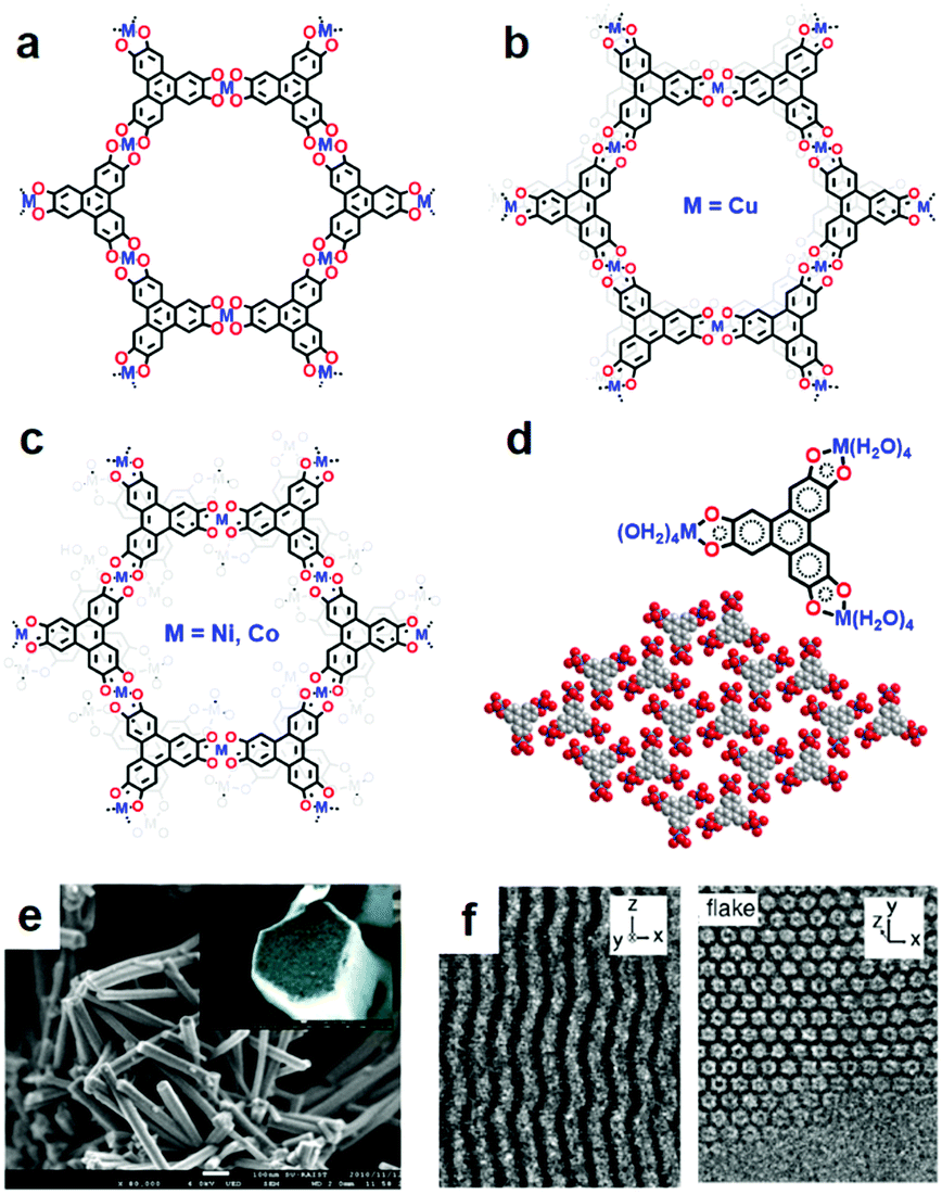 | ||
| Fig. 10 TP-based 2D c-MOFs through hydro-/solvothermal syntheses. (a) Generally displayed structure of Cu3(HHTP)2 and M9(HHTP)4 (M = Ni, Co). (b) Radical structure of bilayer Cu3(HHTP)2. (c) Radical structure of layered M9(HHTP)4 (M = Ni, Co) without counting the water molecules. (d) Structure of trinuclear M3(HHTP)(H2O)12 clusters. (e) SEM image of the nanorod sample. Reproduced with permission ref. 19. Copyright 2012, American Chemical Society. (f) HR-TEM images of Cu3(HHTP)2 nanorods (left) and nanoflakes (right). Reproduced with permission ref. 95. Copyright 2019, American Chemical Society. | ||
In addition to Cu3(HHTP)2, NiN4-linked Ni3(HITP)2 is another representative 2D c-MOF sample. In 2014, Sheberla et al. reported the hydrothermal synthesis of Ni3(HITP)2 based on amine-functionalized TP.57 Upon heating an aqueous solution of HATP and NiCl2 with the existence of NH3·H2O in air, Ni3(HITP)2 was obtained as bulk nanoparticles with an average crystal size less than 200 nm. Monoanionic o-diiminobenzosemiquinonate moieties were confirmed by XPS and elemental analysis, indicative of a charge-neutral network. The further structural analysis revealed the crystal structure of Ni3(HITP)2 with unit cell parameters of a = b = 21.75 Å. In the later studies from the same group, employing NaOAc for the deprotonation, the obtained Ni3(HITP)2 showed superior crystallinity in a rod-like morphology with length of up to 2 μm.58,95 The HR-TEM image of the individual crystal suggested that the Ni3(HITP)2 layers stacked in an almost eclipsed configuration with a periodic interlayer spacing of 3.30 Å. This optimization was also applied to the structurally related charge-neutral Cu3(HITP)2 and Co3(HITP)2 2D c-MOFs.28,58 Meanwhile, HTTP-based MS4-linked (M = Ni, Co, Fe, Pt) 2D c-MOFs were also developed (mainly as films, see Section 4.2),45,64,118 and subsequently great efforts have been devoted to the TP-based 2D c-MOF family with the aim of exploring their multifunctional properties.28,46,59,90,100,106,109,146,147
Towards frameworks with denser distributed ligands and metals, benzene-based ligands were developed.31,39,40,42,74,135 Typically, in 2017, Dou et al. synthesized MN4-linked M3(HIB)2 (M = Cu, Ni) 2D c-MOFs by mixing HAB, M2+, and NH3·H2O in DMSO, followed by heating at 60 °C for 2 hours.40 The obtained samples were formed by irregularly shaped nanoparticles smaller than 100 nm. The backbones were suggested to be charge-neutral, indicative of the existence of same monoanionic o-diiminobenzosemiquinonate moieties as Ni3(HITP)2. Unsurprisingly, N2 adsorption revealed low BET SSA values in the range of 110–150 m2 g−1 due to the increment of the density of ligands and metals in the backbone. Using ethylenediamine as the base under an inert atmosphere, Park et al. reported CuO4-linked Cu3(HHB)2 2D c-MOF nanocrystals (estimated to be <200 nm).39 The authors showed synthetic diversity through the coordination reaction between Cu2+ and either HHB or its derivative tetrahydroxyquinone (THQ). Elemental analysis suggested the presence of protonated ethylenediamine (NH3CH2CH2NH32+) as the counter cation to balance the negative charge of the backbones, which corresponds to a charge state of −1 in each linkage. Analogous to M3(HIB)2, Cu3(HHB)2 exhibited a low BET SSA value of ∼143 m2 g−1. A larger π-conjugated coronene-based building block was introduced for the construction of 2D c-MOFs by our group in 2016.32 The fully thiol-substituted ligand PTC was incorporated into the 2D c-MOF through the coordination with Fe(OAc)2 in an ammoniacal mixture containing deoxygenated water and dimethylformamide (DMF) at 120 °C for 48 hours. Thus, FeS4-linked Fe3(PTC)2 was achieved as an almost non-porous network with crystalline domains up to a dozen of nm. XPS and Mössbauer spectroscopy suggested the presence of Fe3+ species. In addition, we inferred a unit cell with a = b = ∼11.7 Å and an interlayer spacing of ∼3.9 Å for this 2D c-MOF depending on thorough characterization with the support of PXRD, TEM, XPS, and X-ray absorption spectroscopy. Very recently, Yao et al. established a dual-ligand Cu3(HHTP)(HHB) 2D c-MOF with two kinds of ligands of HHTP and THQ in the network.59 Definitely, it was a challenge for the controlled synthesis of this dual-ligand 2D c-MOF by varying various reaction conditions including the temperature, reaction time, ratio of two ligands, and metal salts, in terms of stronger coordination capability of Cu2+ with HHTP than THQ. As a result, the obtained Cu3(HHTP)(HHB) 2D c-MOF presented a morphology of hundreds of nm long nanowires and a unit cell with parameters of a = b = 17.154 Å and c = 6.266 Å for a honeycomb structure. In addition, the charge state of the linkage was −1 with NH3CH2CH2NH32+ as counter ions. The dual-ligand structure shows the great potential of tunability of the porosity and electronic properties.
Utilizing hydro-/solvothermal methodologies, many other 2D c-MOFs based on various building blocks have been constructed, such as Cu3(HHTN)2, Cu3(HHTX)2, Ni3(HIHATNM′3)2, Cu2[DBCO8], M2[M′PcX8], and Ni2[NiNPcO8].33,47–51,53–56,148 In 2019, we employed a modified solvothermal protocol applying vacuum for the synthesis of an oxygen-sensitive system (Fig. 9b): Fe2[FePcO8] 2D c-MOF.33 This method has also been widely employed for vacuum-promoted synthesis of 2D COFs148–150 and 2D non-conjugated MOFs.151 To avoid air-induced oxidation of iron(II) salts, Fe2[FePcO8] was synthesized by mixing FePc(OH)8, Fe(OAc)2, and KOAc (base) in N-methyl-2-pyrrolidone (NMP)/H2O (v/v = 3/1) in a vacuum-sealed tube after thorough deoxygenation by three cycles of freeze–pump–thaw, followed by heating at 150 °C for 3 days. Thus, the obtained Fe2[FePcO8] is comprised of rectangle-shaped crystals in the range of 10–100 nm with a square lattice of a = b = ∼18 Å.
Though hydro-/solvothermal syntheses have been demonstrated as the most effective and simplest strategy for expanding the 2D c-MOF family, this method generally allows barely monitoring or controlling the crystal growth and provides small-sized bulk polycrystals. As a result, integrating the MOF particles into nanodevices and the relevant performance of the thus-far fabricated devices have been largely impeded by the lack of process-capability and accessible active sites as well as sufficient charge carrier transport.
4.2 2D c-MOF films through wet-interface-assisted synthesis
Recently, various bottom-up wet interface-assisted synthetic strategies including gas–liquid (GL), liquid–liquid (LL), and liquid–solid (LS) interfacial approaches have been developed to prepare large-area thin 2D c-MOF films (Fig. 11).21,152–154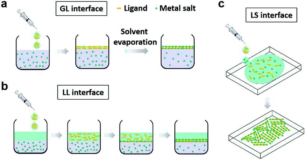 | ||
| Fig. 11 The interfacial strategies for the synthesis of 2D c-MOF films. (a and b) Schematic illustration of gas–liquid and liquid–liquid interfacial methods. (c) Schematic illustration of liquid–solid interfacial synthesis. | ||
One representative work on the synthesis of 2D c-MOF films was reported initially by Kambe et al. in 2013 using a LL interfacial strategy (Fig. 12a).74,75 An organic phase containing HTB in dichloromethane (DCM) was overlaid with an aqueous solution of Ni(OAc)2 and NaBr under an argon atmosphere. The water/DCM interface allowed the formation of a 1–2 μm thick Ni3(HTB)2 2D c-MOF film with a lateral size of ∼100 μm (Fig. 12b). PXRD and TEM analysis (Fig. 12c) indicated a crystal model of Ni3(HTB)2 with parameters of a = b = 14.1 Å and c = 7.6 Å. The same group also reported an isostructural Pd3(HTB)2 using the above LL interfacial method. Additionally, K3[Fe(CN)6] was added as a redox buffer to prevent the reduction of Pd+ to the formation of Pd0.65 In 2015, Huang et al. reported a non-porous 2D c-MOF network Cu3(HTB) (Fig. 12d–f) by coordination of HTB and Cu(NO3)2 at the water/DCM interface.31 The Cu3(HTB) 2D c-MOF was obtained as a continuous film with a lateral size larger than 1 cm and thickness in the range of 20 to 140 nm. In the Cu3(HTB) network, each sulfur atom is coordinated to two copper atoms leading to a non-porous structure with denser ligands and metals. SEM and atomic force microscopy (AFM) images showed a continuously smooth upside in the film whilst the downside composed of plate-like nanosheets was fairly rough, especially for the thick films. The authors suggested that the water/DCM interface functioned initially as a platform for the formation of 2D c-MOF thin films (the upside in the final film), while the HTB ligand functioned as the transporter of the Cu-ions from the interface to the DCM phase below the interface. Then, the Cu-ions coordinated with the HTB molecules below the interface in a less order due to the weaker interface-confining effect here than that at the interface. Grazing incident X-ray diffraction (GIXRD) revealed a face-on orientation of Cu3(HTB) in a 60 nm thick film whilst no preferred orientation was observed for the sample thicker than 200 nm, indicative of randomly accumulated nanocrystals on the downside of the film near the water/DCM interface. Lahiri et al. also employed GL/LL interfacial methods for the construction of M3(HIB)2 (M = Co, Ni, Cu) thin and thick films with thicknesses of 10–13 nm and ∼1 μm, respectively.135
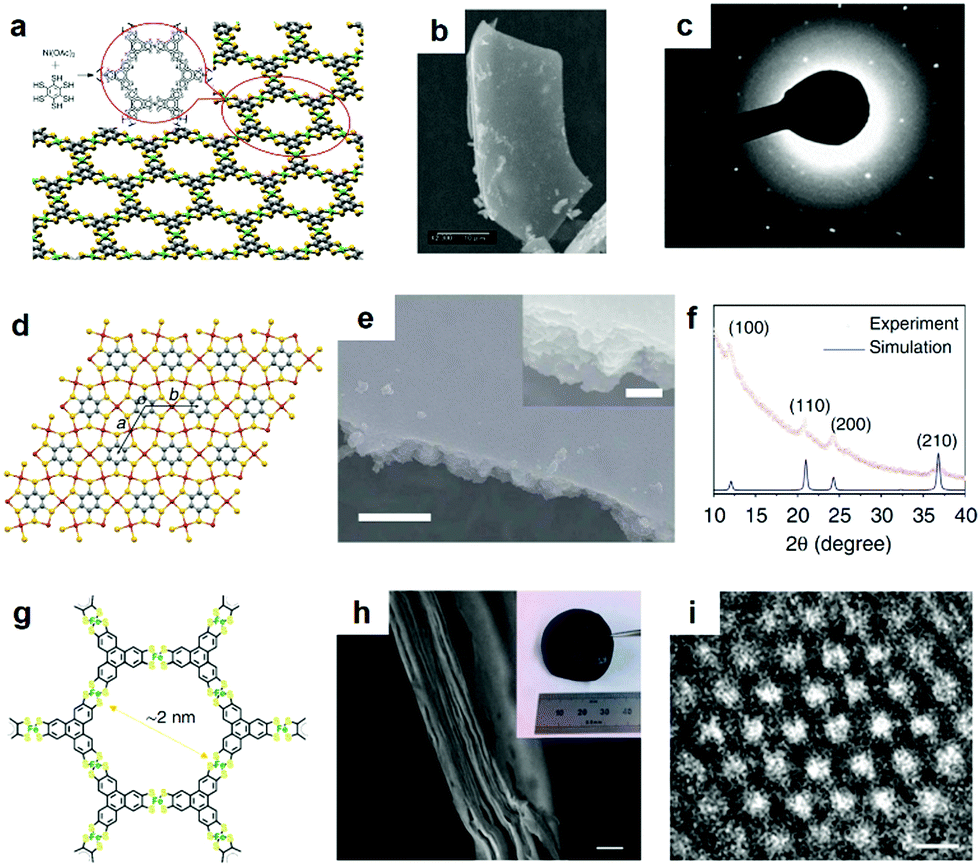 | ||
| Fig. 12 Selected 2D c-MOFs synthesized through the LL interfacial method. (a–c) Ni3(HTB)2 2D c-MOF and its SEM and HR-TEM images. Reproduced with permission ref. 74. Copyright 2013, American Chemical Society. (d–f) Lattice structure of Cu3(HTB) 2D c-MOF and its SEM image as well as in-plane GIXRD pattern.31 Copyright 2015, Nature Publishing Group. (g–i) Fe3(HTTP)2 2D c-MOF and its SEM image from cross-side view and HR-TEM image.78 Copyright 2018, Nature Publishing Group. | ||
In 2016, Wu et al. reported a modified solution synthesis of large-area Ni3(HITP)2 films in a homogeneous aqueous solution of HATP and NiCl2 using trimethylamine as the base under no perturbation.29 Upon heating the mixture to 60 °C, Ni3(HITP)2 nanoparticles self-assembled at the air/water interface and packed further closely to afford a continuous smooth film. The film thickness could reach ∼100 nm after 3 min of polymerization. In 2018, our group demonstrated a LL interfacial synthesis of the Fe3(HTTP)2 2D c-MOF film (Fig. 12g).78 Organic salt of iron(II) acetylacetonate was dissolved in chloroform, which was overlaid by an aqueous phase containing the ligand HTTP and ammonia. Large-area (cm2), free-standing Fe3(HTTP)2 films were obtained with a tunable thickness from 20 nm to ∼2 μm by increasing the reaction time (Fig. 12h and i). TEM imaging revealed that the samples comprised of crystalline domains of ten to hundreds of nm. A honeycomb structure with a pore size of ∼1.9 nm was observed by high-resolution TEM. PXRD displayed (100) and (200) peaks at 2θ = 4.5° and 9.1°, respectively, which demonstrated a honeycomb packing within the ab planes. The (001) reflection (peak at 2θ = 27.3°) suggested an ordered stacking along the c direction with an interlayer distance of ∼0.33 nm. Experimental PXRD patterns agreed well with the simulated inclined AA stacking models. The BET SSA was measured to be ∼526 m2 g−1. In 2019, the above 2D c-MOF film with the thickness ranged from ∼84 to ∼410 nm was also reported by Clough et al. using an ethyl acetate (containing 1% NMP)/water interface.80
Apart from GL and LL approaches, LS interface-assisted synthetic methodology (also termed as on-substrate synthesis, Fig. 11c) has recently emerged for preparing 2D c-MOF films with a preferred face-on orientation, for example, for HHTP-based systems.94,96,155,156 The preliminary on-substrate synthesis was explored by Sheberla et al. by placing a quartz substrate in the reaction mixture for the synthesis of bulk Ni3(HITP)2 2D c-MOFs.57 Ni3(HITP)2 was obtained as a ∼500 nm thick crystallite-accumulated macroscopic film on quartz surface. In 2017, Yao et al. reported a spray layer-by-layer liquid-phase epitaxial method for preparing face-on orientated Cu3(HHTP)2 thin films.96 Typically, –OH functionalized substrates were alternatively exposed to a solution of HHTP and copper(II) acetate in ethanol by a spray method (Fig. 13a and b). The thickness could be controlled from 20 to 100 nm with an average increment of ∼2 nm after each growing cycle. Top- and side-view SEM images reveal a dense and continuous thin film with a moderately smooth surface on the substrate (Fig. 13c). Later on, Mahringer et al. explored a vapor-assisted conversion106 as an effective way for the synthesis of face-on oriented Cu3(HHTP)2 and M9(HHTP)4 (M = Ni, Co) thin films on various substrates.94 The authors utilized an additive of 1-propanol as a modulator for enlarging the crystal size (up to 10 μm for Cu3(HHTP)2, 1–2 μm for Ni9(HHTP)4, and 3–4 μm for Co9(HHTP)4). In a typical synthesis, a water/1-propanol (v/v = 1/1) solution of precursor was spread onto an elevated gold substrate in a reaction vessel containing the vapor source of the same water/1-isopropnaol mixture, and heated at 85 °C for 3 h (Fig. 13d). GIXRD patterns in the in-plane and out-of-plane directions indicated a preferential orientation of Cu3(HHTP)2 or M9(HHTP)4 layers with stacking reflections aligned orthogonally to the surface of the substrates. These samples are free of crack over a large area with thicknesses of ∼200 nm (Fig. 13e). Cross-section SEM images revealed packed pillared crystallites, corresponding to the observation of GIXRD analysis. The LS interfacial synthesis of high quality thin films allows direct device fabrication by adopting conductive or insulating substrates for electronic devices.94,96,97
 | ||
| Fig. 13 Oriented HHTP-based 2D c-MOF films synthesized through various LS interfacial methods. (a) HHTP-based 2D c-MOFs. (b and c) Schematic illustration of the spray layer-by-layer liquid-phase epitaxial method and the SEM image of the obtained Cu3(HHTP)2 film. Reproduced with permission ref. 96. Copyright 2017, Wiley-VCH. (d and e) Schematic illustration of the vapor-assisted conversion method and the top-/side-view SEM images. Reproduced with permission ref. 94. Copyright 2019, American Chemical Society. | ||
Apart from 2D c-MOF thin/thick films and thin nanosheets, the construction of a single-layer sample with high structural control at the atomic level has remained a synthetic challenge. The single-layer sample will offer distinguished properties due to the 2D material nature,157–159 which include, but are not limited to size effects on the intrinsic properties, varied electronic and optical properties due to the absence of interlayer interactions, high exposure of surface active sites, high mechanical flexibility, facile device design and processing, and further construction of multicomponent van der Waals heterostructures.45,61,98,160 In 2015, our group reported the preparation of the first example of large-area, free-standing, single-layer 2D c-MOFs through Langmuir–Blodgett (LB) assisted interfacial synthesis (Fig. 14),161 by controlling the surface pressure (Fig. 15a and b).45
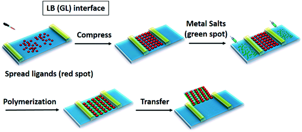 | ||
| Fig. 14 Schematic illustration of Langmuir–Blodgett air/water (a special GL interface) interface-assisted synthesis. Reproduced with permission ref. 21. Copyright 2018, American Chemical Society. | ||
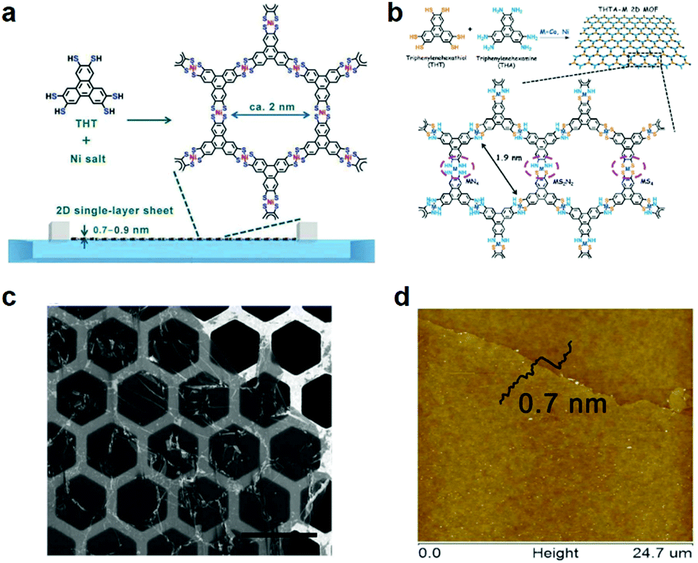 | ||
| Fig. 15 Single-layer 2D c-MOFs synthesized through LB-assisted interfacial synthesis. (a and b) Schematic illustration of the synthesis of Ni3(HTTP)2 and a Co3(HITP)(HTTP) 2D c-MOF comprising mixed ligands of HTTP and HATP. (c and d) SEM and AFM images of single-layer Ni3(HTTP)2. Reproduced with permissions.45,61 Copyrights 2015 and 2017, Wiley-VCH. | ||
Typically, to produce a single-layer Ni3(HTTP)2, a mixed solution of ligand HTTP and DMF/chloroform (v/v = 1/3) was spread over the water surface in a LB trough. Subsequently, the HTTP molecules were compressed into a dense self-assembled monolayer through monitoring and increasing the surface pressure to 10 mN m−1, and an aqueous solution of Ni(NO3)2 was injected into the water phase. With the diffusion of the Ni2+ ions to the air/water interface, a coordination reaction was triggered between HTTP and Ni2+ ions. A free-standing single-layer Ni3(HTTP)2 film was obtained and could be directly transferred onto various substrates for further characterization. The thickness of the film was measured to be ∼0.7 nm by AFM (Fig. 15c and d). As the single-layer sheets showed low stability under electron irradiation, selected area electron diffraction (SAED) was performed by cryogenic TEM at −175 °C, exhibiting a typical hexagonal diffraction pattern. This SAED result at least suggested local crystallinity presenting in the single-layer 2D c-MOF with an ordered honeycomb network having a cell size of ∼2 nm. Such a Ni3(HTTP)2 2D c-MOF was transferred onto glassy carbon electrodes for electrocatalytic water splitting. Currently, due to their well-defined structure and abundant active sites as well as intrinsic conductivity, 2D c-MOFs have been rising as a promising electrode material for electrochemical energy devices.
These efforts from various interfacial approaches allow the integration of 2D c-MOFs into functional devices and thus exploring their multifunctional properties. However, the interfacial strategies have been so far rather limited; the successful synthesis strongly relied on the association of high solubility of selective building blocks in water or organic solvents. In addition, accessibility on controlling/tuning orientation remains to be explored. In addition to wet-surface, the on-surface synthesis using Cu(111) or Au(111) substrates under ultrahigh vacuum provides another pathway to develop a single-layer 2D c-MOF that guarantees a molecular structural resolution with the support of a scanning tunneling microscope (STM).162–165 In 2018, Lischka et al. reported a topologically diverse framework upon annealing HATP on Cu(111). A metal–organic trimer composed of three ligand molecules linked by a Cu3 cluster instead of a single Cu atom was observed, while ring-fused Ni3(HITP)2 with a limited number of repeating units appeared in the presence of additional Ni on Cu(111).163 Later on, by varying Cu(111) surface to Au(111), Gao et al. obtained a monolayer of Ni3(HITP)2 with a domain size of ∼40 nm and resolved its structure at sub-molecular level by STM.162 Recently, Zhang et al. applied the on-surface method for bonding HHB with Cu atoms; however, a single-layer 2D non-conjugated MOF was determined.165 Despite the preliminary success of the on-surface synthesis, many synthetic challenges remain to be addressed, such as the synthesis of large-area (from μm2 to cm2), highly-ordered monolayer networks, the complete lift of the monolayer from the solid surface for device integration, and so on.
5. Device integration based on multi-dispersed 2D c-MOFs
As is shown, 2D c-MOFs have been synthesized by various synthetic methodologies and have shown diverse morphologies, such as bulk powder (polycrystalline nanoparticles or single-crystals) and large-area thin films. Regarding the bulk powders, compressed pellets (Fig. 16a) have been widely employed for device integration (other method e.g. drop-casting, Fig. 16b) and charge transport characterization. Nonetheless, these pellet samples are generally comprised of nanocrystals with no preferred orientation, co-existing with numerous grain boundaries and defects,166 which limited the conductivity performance and the unambiguous understanding on the transport mechanism. By comparison, the single-crystalline 2D c-MOF samples offer the opportunity for device investigation based on each crystal (nanorods or nanoflakes) and allow precise and reliable analysis of the intrinsic electronic properties (Fig. 16c and d). However, the isolated single-crystalline nanorod or nanoflake sample suffers from synthetic challenges and limitation in practical functional studies.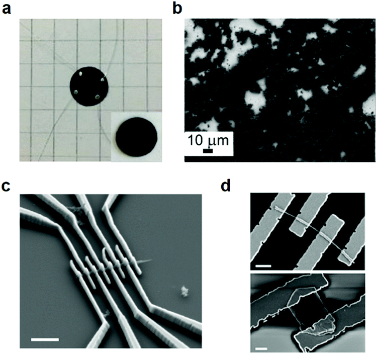 | ||
| Fig. 16 Device integration of bulk 2D c-MOFs. (a) Pellet of 2D c-MOFs and device fabrication in the van der Pauw geometry.55 Copyright 2020, Wiley-VCH. (b) SEM image of drop-cast Cu3(HITP)2 on an indium-tin-oxide glass slide. Reproduced with permission ref. 28. Copyright 2015, Wiley-VCH. (c) SEM image of the fabricated device based on isolated single-crystalline Ni3(HITP)2 nanorods. (d) SEM images of fabricated devices based on isolated single-crystalline Cu3(HHTP)2 nanorods (top) and nanoflakes (down). Reproduced with permission ref. 95. Copyright 2019, American Chemical Society. | ||
In regard to addressing the above challenges with respect to application of the bulk crystals (polycrystals and single-crystals) obtained by the hydro-/solvothermal syntheses, top-down exfoliation through methods such as ball-milling167,168 and sonication144,145,169 (Fig. 17a) is expected to be an efficient approach to achieve thin nanosheets,169–172 which can maintain the intrinsic conductivity and porosity, allow high exposure of active sites, as well as facile solution-processible device integration.173 Currently, few top-down methods have been applied to the delamination of bulk 2D c-MOFs.
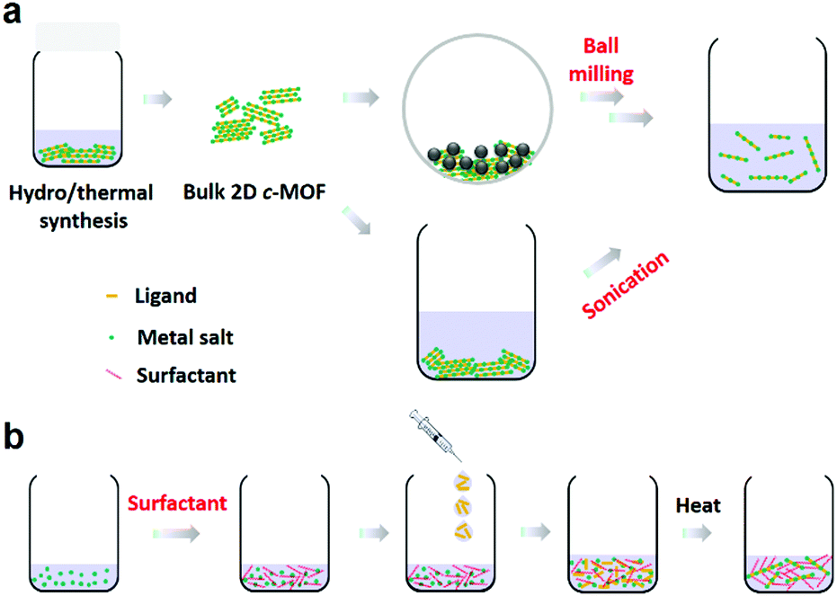 | ||
| Fig. 17 Schematic illustration of the synthesis of 2D c-MOF nanosheets through top-down and bottom-up method. (a) Top-down ball milling and sonication exfoliation. (b) Bottom-up surfactant-assisted synthesis. | ||
Very recently, we employed ball milling exfoliation for the synthesis of Ni2[CuPc(NH)8] 2D c-MOF nanosheets.55 Firstly, a highly crystalline bulk Ni2[CuPc(NH)8] sample was prepared with an average domain size of ∼200 nm via a solvothermal protocol. Then, via a NaCl-assisted low energy ball milling strategy (Fig. 18a), bulk Ni2[CuPc(NH)8] nanocrystals were mechanically exfoliated into nanosheets with a yield of 40–50%. PXRD patterns revealed a shift of the layer distance from 3.24 to 3.33 Å, indicative of swollen layers after milling. SEM, AFM and HR-TEM together indicated an average lateral size of ∼160 nm and a thickness of ∼7 nm for these nanosheets (Fig. 18b). The achieved nanosheets could be homogeneously dispersed in DMF for more than six months that allows facile solution-processible micro-supercapacitor device fabrication through filtration (further discussion is in Section 6.5.2).
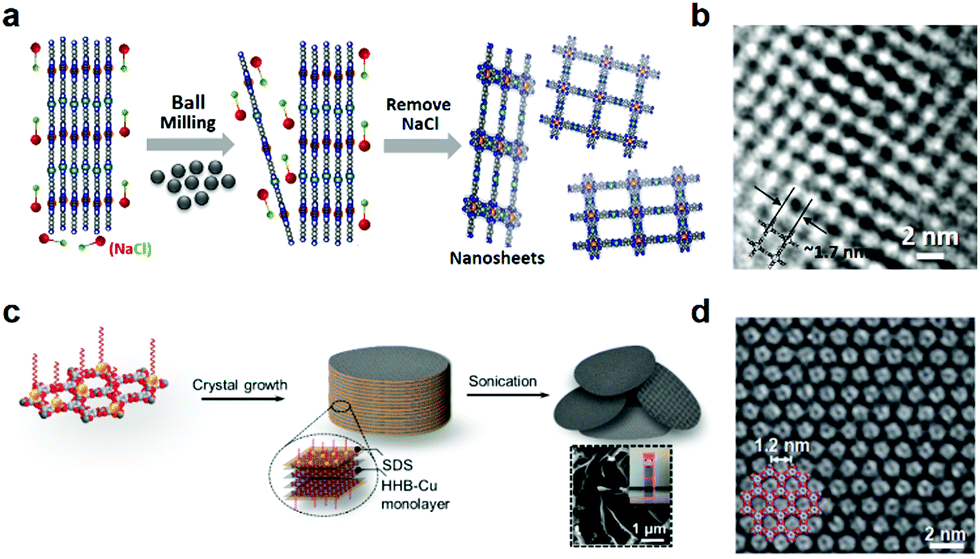 | ||
| Fig. 18 Synthesis of 2D c-MOF nanosheets. (a and b) Schematic illustration of the NaCl-assisted ball-milling exfoliation of Ni2[CuPc(NH)8] and HR-TEM image of the synthesized nanosheets.55 Copyright 2020, Wiley-VCH. (c and d) Schematic illustration of surfactant-assisted synthesis of Cu3(HHB)2 2D c-MOF nanosheets and the related HR-TEM image.88 Copyright 2020, the Royal Society of Chemistry. | ||
Even though the top-down exfoliation method offers a possibility in scalable synthesis of nanosheets with accessible active sites and solution-processibility, it remains limited in the control of the morphology, the layer numbers and the lateral domain size. By contrast, bottom-up methods that refer to the direct synthesis of the nanosheets from metal nodes and ligands hold promise in the synthesis of high-quality 2D c-MOF nanosheets. Recently, our group introduced a surfactant-mediated synthetic method toward single-crystalline Cu3(HHB)2 nanosheets (Fig. 17b).88 The sodium dodecyl sulfate (SDS) anionic surfactant was used as the directing agent for restricting the growth of 2D c-MOFs along the c direction and weakening the interlayer interactions.174,175 In a typical surfactant-mediated hydrothermal synthesis, the precursors of THQ, Cu(OAc)2, and NaOH (base) in a SDS aqueous solution were ultrasonicated at 50 °C to prepare the nanosheets with an ultrahigh yield of 80–90% (Fig. 18c). As a consequence, the achieved nanosheets presented a thickness of 4.2 ± 1.1 nm and a lateral size of 0.30–0.65 μm2, as well as a much higher BET SSA (385 m2 g−1) than the contrast powder sample (119 m2 g−1) obtained in the absence of SDS. HR-TEM and related SAED analysis demonstrated the achievement of single-crystalline nanosheets without noticeable defects (Fig. 18d). The high exposure of active sites in the nanosheet sample allows fast ion/electron diffusion hence ensuring superior performance than the related bulk Cu3(HHB)2 as an electrode material (Section 6.5.1).
Synthesis of solution-processible nanosheets will be facile for the fabrication of 2D c-MOF based devices via spin-coating, filtration, ink-printing, etc. In this respect, it requires to address the key questions on the homogeneous dispersion in solution and the control of size, thickness and crystallinity as well as avoiding the re-stacking during solidification. Definitely, another choice is to utilize the free-standing, large-area, highly crystalline 2D c-MOF thin films with tunable thickness, which will simplify the device fabrication by direct deposition onto the substrates. To this end, an extraordinary property and a reliable structure–property relationship are expected, thus pushing the functional development for MOFtronics.
6. Functions for MOFtronics
Conductive 2D c-MOFs possess a series of unique features, such as large surface to volume ratio, defined active sites, and tailored electronic structure that enables a set of intriguing properties from semiconductor and redox activity to metallicity, ferromagnetism, photoswitching, etc. High conductivities in 2D c-MOFs have attracted great attention in various MOFtronics including (opto)electronics, spintronics, and thermoelectrics, as well as energy storage devices as potential power sources for MOFtronics.6.1 Electronics
The emerging 2D c-MOFs featuring semiconductor properties, high conductivity, and electrically-transduced sensing have been expected to be outstanding substitutes for potential applications in electronics, such as field-effect transistors, superconductors, chemiresistors, etc.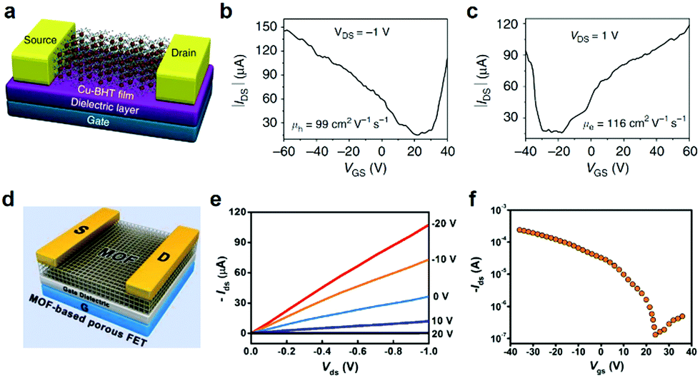 | ||
| Fig. 19 2D c-MOF based FET devices. (a–c) Illustrative schematic of FET based on Cu3(HTB) and related transfer characteristics.31 Copyright 2015, Nature Publishing Group. (d) Ni3(HITP)2-based FET. (e and f) Output curves and transfer characteristic plot of Ni3(HITP)2, respectively. Reproduced with permission ref. 29. Copyright 2017, American Chemical Society. | ||
The porous and tailored structure of 2D c-MOFs ensures the diversity of their FET devices. However, many challenges remain to date, such as the formation of the 2D c-MOF film with high smoothness and controllable thickness, tunability of band gaps, optimized integration for good contacts, etc.
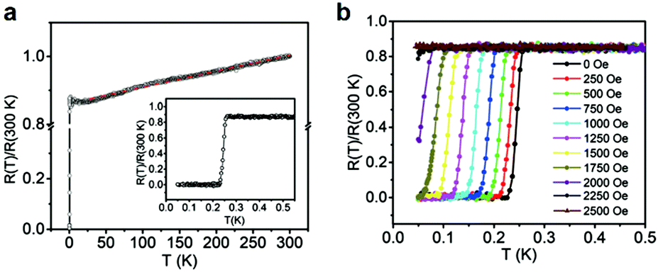 | ||
| Fig. 20 Superconductivity of Cu3(HTB). (a) Temperature-dependence of the normalized resistance from 0.05 to 300 K of Cu3(HTB). (b) Temperature-dependence of the normalized resistance of Cu3(HTB) in applied magnetic fields up to 2500 Oe. Reproduced with permission ref. 68. Copyright 2018, Wiley-VCH. | ||
2D c-MOF based chemiresistors were demonstrated by Campbell et al. in 2015 initially.28 Bulk Cu3(HITP)2 2D c-MOF was transferred onto interdigitated gold electrodes by drop-casting an acetone dispersion of Cu3(HITP)2 to construct the device. The chemiresistor was capable of detection of NH3 in parts per million (ppm) concentration level at room temperature, in spite of the existence of 60% relative humidity (RH) (Fig. 21a and b). However, the isostructural Ni3(HITP)2 2D c-MOF did not produce any reliable response under identical conditions, indicating the impact of rational modification on metal nodes on the functionality. Later on, Mirica's group reported the utilization of Cu3(HHTP)2 and M9(HHTP)4 (M = Ni, Co) 2D c-MOFs for the detection of NH3 by preparing the 2D c-MOF/graphite hybrids92 or assembling the 2D c-MOFs on graphitic electrodes176 through the typical hydrothermal method. In 2018, combining experiment with simulation, Rubio-Gimenez et al. ascribed the origin of response of Cu3(HHTP)2 toward NH3 to the coordination of NH3 to Cu2+ in the network.122 Kelvin probe measurements revealed the difference of work function after exposing Cu3(HHTP)2 to NH3, and infrared (IR) reflection absorption spectroscopy indicated the appearance of NH3 stretching bands and the coordination between NH3 and Cu atom in Cu3(HHTP)2. According to the simulation, the coordination leads to slight distortions of the electronic structure and triggers an increase in the band gap from 0.33 to 0.42 V. Yao et al. integrated the Cu3(HHTP)(HHB) 2D c-MOF into a gas sensor by the drop-casting method which showed good sensing performance for NH3 in the concentration range of 1–100 ppm.59 IR spectroscopy and PXRD spectroscopy revealed the NH3–Cu+/2+ interaction with an expanded c lattice upon exposure to NH3. Important advancement was reported by Xu and co-workers using the high quality Cu3(HHTP)2 thin film prepared through the LS interfacial approach.96 The resulting sensor exhibited a high response of 129% and >10% toward 100 and 1 ppm of NH3 vapor, respectively (Fig. 21c). The authors calculated the theoretical limit of detection (LOD) to be ∼0.5 ppm by setting the response as 10%. In addition, the response and recovery were accelerated by 54% and 10% respectively compared with those of the corresponding bulk Cu3(HHTP)2 based sensor.
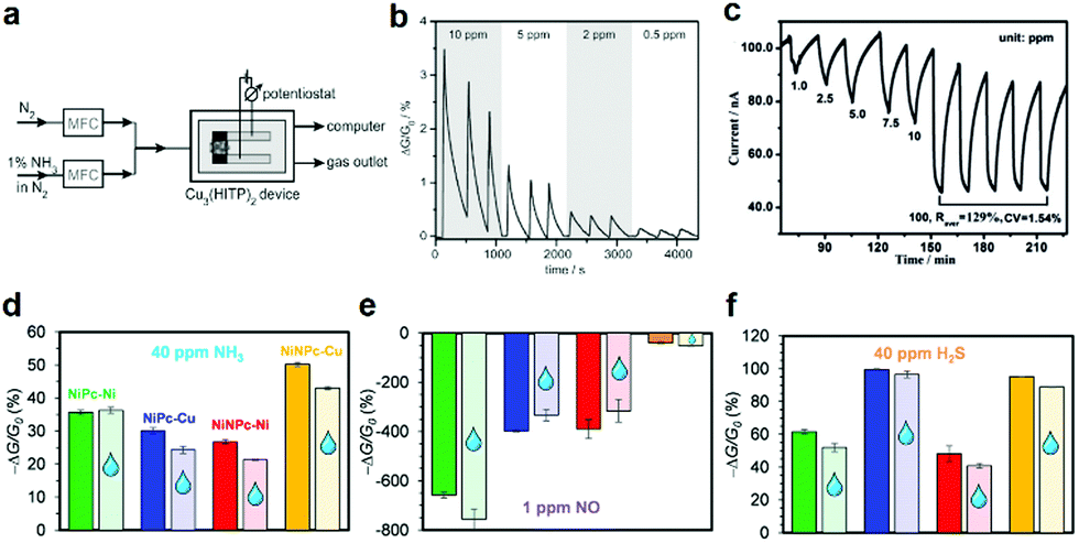 | ||
| Fig. 21 2D c-MOF based chemiresistors for the detection of NH3, NO, and H2S. (a and b) Schematic of the experimental apparatus and relative response curve of Cu3(HITP)2 toward NH3 at different concentrations. Reproduced with permission ref. 28. Copyright 2015, Wiley-VCH. (c) The response–recovery curve of the Cu3(HHTP)2 thin film toward NH3 at different concentrations. Reproduced with permission ref. 96. Copyright 2017, Wiley-VCH. (d–f) Sensing responses of M2[NiPcO8] and M2[NiNPcO8] (M = Cu, Ni) upon 30 min exposure to 40 ppm of NH3, H2S, and 1 ppm of NO in dry nitrogen and in the presence of H2O. Reproduced with permission ref. 51. Copyright 2019, American Chemical Society. | ||
Besides NH3, Mirica and co-workers demonstrated Cu3(HHTP)2 and Ni9(HHTP)4 2D c-MOFs as the active materials for the chemiresistive response to other toxic gases including NO and H2S.176 The same group integrated Ni9(HHTP)4 or Ni3(HITP)2 into textile-supported gas sensors for the detection of NO and H2S, which exhibited good mechanical flexibility.102 The sensors were able to detect NO and H2S with high performance in the presence of humidity (18% RH) and were fully recoverable after washing the devices with water. Recently, Meng et al. reported chemiresistive sensors based on a series of phthalocyanine derivatives-based 2D c-MOFs (M2[NiPcO8] and M2[NiNPcO8], M = Cu, Ni).51 The resulting devices displayed outstanding humidity-independent ability during the detection and differentiation of NH3, H2S, and NO, and delivered sub-ppm or part-per-billion (ppb) level theoretical LODs at room temperature (Fig. 21d–f).
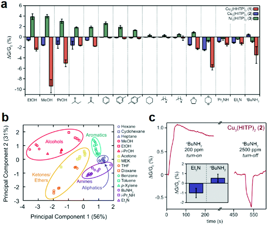
In 2015, Campbell et al. contributed to a cross-reactive sensor array, which was capable of distinguishing five categories of volatile organic compounds (VOCs) (alcohols, amines, ketones/ethers, aromatic and aliphatic hydrocarbons) (Fig. 22a and b).91 Structurally analogous Cu3(HHTP)2 and M3(HITP)2 (M = Cu, Ni) 2D c-MOFs were applied for the fabrication of sensors through drop-casting. These 2D c-MOF based devices exhibited diverse sensing behaviors toward various VOC vapors at a concentration of 200 ppm. Both varying the metal nodes and ligands led to changes in the response to each gas. Furthermore, all samples delivered a high response to polar VOCs, while no appreciable signals were recorded for the aliphatic hydrocarbons. The authors noted both “turn-on” and “turn-off” responses of Cu3(HITP)2 for nBuNH2 at 200 and 2500 ppm respectively (Fig. 22c) and speculated a multiple sensing mechanism including charge transfer and hydrogen bonding among these 2D c-MOFs. Later on, Hoppe et al. prepared a 1–3 μm thick Cu3(HHTP)2 film by spray-coating its dispersion on glass slides or flexible polycarbonate foils and fabricated chemiresistive sensors for methanol sensing accordingly.93
 | ||
| Fig. 22 2D c-MOF based chemiresistors for the detection of VOCs. (a and b) Sensing responses and related principal component analysis to various 200 ppm of VOC vapors for the 2D c-MOF array: M3(HXTP)2 (M = Cu, Ni; X = O, NH). (c) Sensing response for Cu3(HITP)2 to nBuNH2. Reproduced with permission ref. 91. Copyright 2015, American Chemical Society. | ||
Besides conventional analytes, the groups of Mirica and Dincă have applied 2D c-MOFs for the detection of ions (Cu3(HHTP)2, and M9(HHTP)4)177 and CO2 (Cu3(HIB)2),178 respectively. Despite numerous successful examples of 2D c-MOFs for sensors, the thus-far fabricated gas sensors through the compressing or drop-casting method based on bulk 2D c-MOFs obtained by solvothermal synthesis, have brought difficulties in realizing the mass production of devices and exhibited limited performance. Analogous to FETs, the rational tuning of the electronic and chemical structures, improving the quality of thin 2D c-MOF films, and further optimizing the integration methods thus leading to high performance remain to be explored. Moreover, fundamental understanding of the sensing mechanisms such as analyte-metal coordination, hydrogen bonding interaction, and guest–host interaction to ascertain neat structure–property relationship requires under investigation.
6.2 Optoelectronics
Conductive 2D c-MOFs with tailorable band gaps are appealing materials for optoelectronics, such as photodetectors, organic light-emitting devices, solar cells, etc.30,143,179 Very recently, we and cooperation partner demonstrated a Fe3(HTTP)2 based two-terminal photodetector device operated in photoconductive mode (Fig. 23a).30 The record-high mobility and band-like charge transport of Fe3(HTTP)2 allow effective transduction of generated signals. The related device was capable of detecting light ranging from UV to NIR range (400–1575 nm). At room temperature, due to thermally activated band-to-band population of charge carriers in this active material, the Fe3(HTTP)2 possessing a narrow IR band gap of ∼0.45 eV displayed limited performance. Cooling the devices to 77 K suppressed this thermal excitation hence leading to a stronger response and higher sensitivity (Fig. 23b–d). Upon 785 nm excitation at 77 K, a lower noise equivalent power was achieved with a specific detectivity of 7 × 108 cm Hz1/2 W−1. | ||
| Fig. 23 Fe3(HTTP)2 2D c-MOF based photodetector. (a and b) Schematic of a two-terminal photodetector device based on 1.7 μm thick Fe3(HTTP)2 and its dependence of detectivity at −1 V bias. (c) Temperature-dependent photoresponse versus time. (d) Zoomed time-resolved response at 77 K showing a response time of ∼2 s.30 Copyright 2020, Wiley-VCH. | ||
6.3 Spintronics
Merging high conductivity and long range magnetic ordering are highly desirable in spintronics for data storage and processing, such as spin transistors,180 spin Hall effect transistors,181 spin photovoltaic,182 spin valves,183etc. The traditional active materials such as inorganic compounds or organic/molecular film semiconductors have displayed high performance. Nevertheless, the inorganic compounds and organic/molecular film semiconductors are facing the challenge of lack of tunability in magnetic/conductive properties or adequacy in sufficient mobilities, respectively.32 By contrast, in-plane fully π-conjugated 2D c-MOFs with structural diversity and high charge transport enable the interaction between the carriers and localized spins, hence providing promise of tunable magnetic ordering.32,67,184 | ||
| Fig. 24 Spin-properties of 2D c-MOFs. (a–c) Fe3(PTC) 2D c-MOF and its ferromagnetic ground state, magnetic hysteresis loops at different temperatures, as well as field-cooled (FC)/zero-field-cooled (ZFC) magnetization as a function of temperature at an applied field of 100 Oe.32 Copyright 2018, Nature Publishing Group. (d–f) Fe2[FePcO8] 2D c-MOF and its magnetic hysteresis loops at different temperatures, ZFC/FC magnetization at 100 Oe.33 Copyright 2019, Nature Publishing Group. (g and h) Diagram of the Cu3(HHTP)2 based vertical OSV and its magnetoresistance loop for at 10 K. Reproduced with permission ref. 97. Copyright 2020, Wiley-VCH. (i) Schematic illustration of lateral spin valves. | ||
The contribution of strong π–d hybridization and strong π-conjugation to the charge transport along the entire network remains an open question. Nevertheless, we noted their influence on the extraordinary magnetic ordering among 2D c-MOFs. We also consider that both studies utilizing bulk materials did not exclude the impact of the grain boundaries, defects, edges, or the crystallite tilting on the magnetic properties. Improving the crystallinity to achieve single-crystals or single domain films will benefit the understanding of intrinsic magnetic properties and realizing ferromagnetism even at/above room temperature.
However, the porous structure of Cu3(HHTP)2 as a spacer in a vertical spin device may affect its long-term practicability due to the potential inter-diffusion of the upper electrode material of Co through the 1D channel of Cu3(HHTP)2 to the LMSO electrode at the bottom.190 Therefore, non-porous networks for preventing the penetration are more reasonable. Instead, the lateral architecture represents another approach for the integration of porous 2D c-MOFs into spintronic devices (Fig. 24i).
6.4 Thermoelectrics
The porous structure of 2D c-MOFs makes them great candidate for thermoelectric applications because the pores are capable of scattering phonons strongly.105,110 In 2017, Sun et al. applied Ni3(HITP)2 to the investigation of its thermoelectric properties though a pellet sample.105 The device of the pellet showed an ultralow thermal conductivity of 0.21 W m−1 K−1 and a high thermoelectric figure of merit (ZT) of 1.19 × 10⁻³ at 25 °C. The ZT value increased 17-fold compared with traditional 7,7,8,8-tetracyanoquinodimethane-infiltrated Cu3(benzene-1,3,5-tricarboxylate)2 (Cu3 (BTC) 2-TCNQ) MOF based thermoelectric device. The room temperature conductivity of 58.8 S cm−1 correlates to an electronic (κe) contributed thermal conductivity of 4.28 × 10⁻³ W m−1 K−1, hence suggesting a lattice dominated thermal transport in this 2D c-MOF.Up to here, despite the great progress of 2D c-MOFs for (opto)electronics, spintronics, and thermoelectrics, the current studies in these fields rely largely on TP-based 2D c-MOFs, due to the contributions of diverse synthetic methodologies for the TP-based systems. The development of MOFtronics towards other 2D c-MOF systems is still in its infancy. In-depth understanding on producing/integrating methods and exploring active materials with appropriate conductivity and band structure merits further exploration.
6.5 Electrochemical energy storage devices
Conductive 2D c-MOFs incorporating triphenylene-type monomers and abundant quinone-species, such as o-benzosemiquinonate and o-diiminobenzosemiquinonate (Fig. 7),36,40,51,56,57,191 have emerged as a novel class of multifunctional electrode materials for electrochemical energy storage. Among plenty of technologies,104,192–196 metal-ion batteries and supercapacitors represent two major energy storage devices.195 Benefiting from the intrinsically conductive and porous properties, 2D c-MOFs have shown excellent performance in metal-ion batteries and supercapacitors, which could function as the power sources for the above mentioned MOFtronics.197–201 | ||
| Fig. 25 Selected 2D c-MOF based metal-ion batteries. (a) Applied M3(HXB)2 2D c-MOFs for metal-ion batteries. When M = Cu, X = O, the charge state is −1. (b) The charge/discharge curves and cycling stability test of Ni3(HIB)2 in a Li-ion battery. Reproduced with permission ref. 36. Copyright 2018, Wiley-VCH. (c) Utilization of Cu3(HHB)2 thin nanosheets in Li-ion batteries and the charge/discharge curves.88 Copyright 2020, the Royal Society of Chemistry. (d) Illustration of Cu3(HHTP)2 based aqueous Zn-ion battery.89 Copyright 2019, Nature Publishing Group. (e and f) M2[CuPcO8] as the host in a Na–I2 battery and its electrochemical performance, the calculated capacitive contribution of the Fe2[CuPcO8]/I2 electrode as well as the cycling stability.203 Copyright 2020, Wiley-VCH. | ||
Although Li/Na-ion batteries have been extensively studied, the high cost and safety issues impede further development. Instead, less toxic and cheaper aqueous zinc batteries are a good alternative. Recently, Nam et. al. developed a Cu3(HHTP)2 based Zn-ion battery (Fig. 25d) with a high capacity of 228 mA h g−1.89 The authors identified the role of H2O in the performance. In an aqueous electrolyte of a 3 M aqueous solution of Zn(CF3SO3)2, the hydrated Zn2+ was allowed to be inserted into the 1D channels in the backbone with a high diffusion rate during discharge. As contrast, significantly higher interfacial resistance and a lower capacity of 144 mA h g−1 were recorded for the organic electrolyte.
Apart from serving as active materials, our group has explored 2D c-MOFs as the host for the non-conductive cathode material of iodine (I2) in Na–I2 batteries.203 M2[CuPcO8] (M = Fe, Ni, Zn) were selected for hosting iodine and resolving the poor cycle stability of the I2 cathode due to the dissolution of polyiodide in the electrolyte. The MO4 linkages were confirmed to be effective for iodine adsorption; amongst, FeO4 possessed the highest efficacy. The constructed Fe2[CuPcO8]/I2 electrode delivered a high discharge capacity of 208 mA h g−1 and outstanding cycling stability with almost no capacity decay after 3200 cycles (Fig. 25e and f).
 | ||
| Fig. 26 EDL capacitors based on 2D c-MOFs. (a) Schematic of the accommodation of electrolyte ions in 2D c-MOF. (b) Schematic of the diffusion of electrolyte ions into various 2D c-MOFs with different sized 1D channels. (c) Cu3(HHTP)2 on carbon fiber paper for supercapacitors, which powered a red light-emitting-diode. Reproduced with permission ref. 90. Copyright 2017, Wiley-VCH. | ||
Apart from the conventional supercapacitors,206,207 efforts have been devoted to flexible micro-supercapacitors (MSCs) as well, which are promising micro-power sources for next-generation portable electronic devices.208–211 Very recently, Wu et al. applied laser scribing technique assisted solvothermal synthesis to interdigitate Ni9(HHTP)4 on 3D porous laser scribed graphene (LSG) on a polyimide (PI) substrate.100 A CO2 laser was applied for patterning LSG, followed by O2-plasma treatment to serve as a current collector and the platform for the deposition of Ni9(HHTP)4 (Fig. 27a and b). The hybrid delivered areal capacitance, energy density, and power density of 15.2 mF cm−2, 4.1 μW h cm−2, and 7 mW cm−2, respectively. Benefiting from the ultrathin feature of our exfoliated Ni2[CuPc(NH)8] nanosheets (Section 5) that allow facile solution-processibility through filtration, flexible MSC devices were constructed based on Ni2[CuPc(NH)8]/graphene hybrids on PI as film electrodes in a PVA/LiCl gel electrolyte (Fig. 27c).55 The MSC device exhibited high areal capacitance and power density of 18.9 mF cm−2 and 168 mW cm−2 respectively as well as excellent cycling stability. Even on alternating the flat and bent states, the device still maintained 86.2% of the initial performance after 3000 cycles (Fig. 27d).
 | ||
| Fig. 27 2D c-MOFs based MSCs. (a and b) Illustration of LSG-supported Ni9(HHTP)4 for MSC and its SEM image. Reproduced with permission ref. 100. Copyright 2019, Wiley-VCH. (c and d) Flexible MSC device based on Ni2[CuPc(NH)8] nanosheets.55 Copyright 2020, Wiley-VCH. | ||
Beside EDL storage, 2D c-MOFs have displayed pseudo-capacitive charge storage25,26 in aqueous electrolytes, which differs from the EDL mechanism and involves surface reversible faradaic redox reactions.206 The incorporation of the pseudo-capacitive storage with redox reactions generally leads to enhancement in gravimetric and volumetric capacitances. In 2018, Feng et al. reported pseudo-capacitors based on Cu3(HIB)2 and Ni3(HIB)2 in 1 M KOH aqueous electrolyte.38 The reversible pseudo-capacitive behaviors enabled Cu3(HIB)2 and Ni3(HIB)2 pellets to present a high gravimetric capacitance of 215 and over 400 F g−1, respectively, while the contribution of EDL capacitances was estimated to be less than 20% and 10%, respectively. A 50 μm thick Ni3(HIB)2 exhibited an excellent volumetric capacitance up to 760 F cm−3. By further thickening it to 360 μm, the volumetric capacitance was revealed to be 460 F cm−3 and an areal capacitance was determined to be 17 F cm−2. In addition, similar to those metal-ion batteries,35,36 the redox reaction in Ni3(HIB)2 was speculated to be ligand-based,37 as evidenced by a set of redox peaks from the ligand and excluded valence change of Ni atoms by XPS. Pseudo-capacitive behavior was further exemplified by the DBC-based Cu2[DBCO8] 2D c-MOF.56 In a 1 M NaCl aqueous electrolyte, Cu2[DBCO8] displayed a nearly rectangular cyclic voltammetry curve with distinct redox peaks, indicative of both EDL and pseudo-capacitance for this material with estimated contributions of 62 and 38%, respectively. The supercapacitor provided high areal and volumetric capacitances of ∼0.9 F cm−2 and 22 F cm−3 respectively in solid-state.
As demonstrated, owing to the high intrinsic porosity and abundant redox active linkages, 2D c-MOFs have been integrated into multifunctional electrochemical energy storage devices. Hybridization212–216 of 2D c-MOFs with other materials has been proved to be an approach for advancing the performance. Accordingly, various templates, such as carbon fiber paper,90 cellulose nanofibers,101 graphene,100 copper metal,217 and polypyrrole membrane146 have been utilized as platforms for the deposition of 2D c-MOFs. However, these samples are not structurally defined 2D c-MOFs anymore and exclude a neat structure–property relationship. Overall, the current studies provide guidelines corresponding to the rational design of chemical structure and modulation on the porosity and pore size.
7. Conclusions and outlook
In this review article, we introduce the diversity of the chemical structures of 2D c-MOFs based on various conjugated building blocks including benzene, triphenylene, trinaphthylene, truxene, hexaazatrinaphthylene, coronene, phthalocyanine, naphthalocyanine, and dibenzo[g,p]chrysene with ortho-substituted functional groups (–OH, –NH2, –SH, and –SeH). In addition, the multicomponent 2D c-MOFs comprising mixed ligands (e.g. Cu3(HHTP)(HHB)) or mixed metals (e.g. MnM′3−n(HITP)2) show great potential of tunability of the porosity, active sites, and electronic properties. The chemical tunability endows 2D c-MOFs with unique chemical and physical features, such as crystallinity, porosity, stability, tailorable band gaps, electrical conductivity, photoactivity, magnetic ordering, and topological state, thereby offering 2D c-MOFs great potential for broad applications in multiple MOFtronics. In this context, based on the thus-far reported examples, we provide an overview of the monomer/2D c-MOF design, controlled synthesis, device integration, and multifunction of 2D c-MOFs.More specifically, we discuss the structure–electronic property relationship by considering the influence of molecular design (type and geometry of ligand, metal) and material structure (redox-activity in linkage, layer stacking and arrangement) as well as crystallinity. We further summarize the conductivities and mobilities for thus-far reported 2D c-MOFs, which reach 2500 S cm−1 (Cu3(HTB), measured by 4-probe configuration) and 220 cm2 V−1 s−1 (Fe3(HTTP)2, hole mobility measured by Hall effect and TRTS) respectively at room temperature. Theoretically, DFT calculations demonstrated that 2D c-MOFs are expected to exhibit some nontrivial physical properties, such as topological state (single-layer of Ni3(HTB)2), high-temperature ferromagnetic ordering (Curie temperature of 170, 212, and 450 K for single-layer of Ni2[MnPc(NH8)], Mn3(HTB)2, and Mn3(HIB)2, respectively).34,84,85 Experimentally, various synthetic methodologies have been applied to the development of 2D c-MOFs as bulk powder (hydro-/solvothermal method) or film (wet-interface-assisted method) samples. The hydro-/solvothermal method is a straightforward strategy that allows diversity in the reaction conditions and offers large scale and high yield synthesis. Besides the generally obtained morphology of 2D c-MOFs as nanocrystals <100 nm, this method also provides the possibility to synthesize moderate-sized single-crystals (1–10 μm). Among the reported systems, we highlight the significance of single-crystalline nanorods (e.g. Cu3(HHTP)2, Ni3(HITP)2) and nanoflakes (e.g. Cu3(HHTP)2, Cu3(HHB)2) on unambiguous understanding of the charge transport properties/mechanisms of 2D c-MOFs. By comparison, the wet-interface-assisted strategies including gas–liquid, liquid–liquid, and liquid–solid interfacial approaches show promise in constructing large-area, free-standing 2D c-MOF thin films, which ensure sufficient charge transport and facile device integration and hold potential for the realization of practical application of this class of materials for MOFtronics. Particularly, we highlight the construction of single-layer of 2D c-MOFs (e.g. Ni3(HTTP)2, at the LB air/water interface), which is beneficial to the high exposure of active sites and excellent processibility. Next, device fabrications based on the obtained bulk or film samples are presented. To address the processing challenges faced by the bulk crystals, top-down exfoliation and bottom-up surfactant-assisted synthesis achieving homogeneous nanosheets in solution are considered as efficient strategies to provide accessible active sites and solution-processibility.
Finally, we introduce the broad application of conductive 2D c-MOFs for MOFtronics covering (opto)electronics (e.g. FETs, superconductors, chemiresistors, photodetectors), spintronics (e.g. ferromagnetic semiconductors, spacers), and thermoelectrics, as well as the utilization of 2D c-MOFs as potential power sources for MOFtronics including battery and supercapacitor devices. Owing to the unique features of 2D c-MOFs combining large surface to volume ratio, defined active sites, and tailored electronic structure with high conductivity, photoactivity, or high-temperature ferromagnetic ordering, we especially emphasize the great potential of 2D c-MOFs for superconductors, photodetectors, and ferromagnetic semiconductors.
In addition to the foregoing applications, 2D c-MOFs are also potential alternatives to traditional electrocatalysts for promoting the reactivity and fundamentally understanding the mechanism218–221 in various electrochemical energy conversion reactions.222–229 MO4- and MS4-linkages have been widely demonstrated as the active sites towards the hydrogen evolution reaction45,49,61,62,118,230,231 and oxygen evolution reaction.54,160,232,233 For instance, the constructed single-layer of Ni3(HTTP)2 exhibited an overpotential of 333 mV.45 Apart from water splitting, 2D c-MOFs have emerged as model catalysts to investigate the mechanism during the oxygen reduction reaction.52,99,103,234–238 For instance, Co2[CuPcO8] delivered excellent activity with a half-wave overpotential of 830 mV, under a four-electron O2 reduction process.53 In regard to the emerging carbon dioxide reduction reaction (CO2RR), based on an array of M2[M′PcO8] (M = Cu, Zn; M′ = Cu, Zn) 2D c-MOFs with finely tuned active sites, our group has established a structure–property relationship regarding the selectivity of active sites toward carbon dioxide reduction or the concomitant hydrogen evolution.53 Regardless of the preliminary success, the study towards complicated reactions such as CO2RR is still at infancy, and in-depth investigation on the mechanisms remains of growing interest. In the past few years, 2D c-MOFs stand out for electrochemical molecular capture109 and detection239,240 as well.
The development of 2D c-MOFs discussed here leaves no doubt that the extension of this class of materials to MOFtronics is of substantial interest to the next generation of logic and memory devices. In this context, it is important to clarify that the traditional photo-/electroactive materials should not be the metric for 2D c-MOFs and MOFtronics. 2D c-MOFs may outperform traditional electronic materials, but, this judgement cannot be true without specifying the particular property and device/technique type. For instance, the intrinsic room-temperature mobilities of electrons and holes for crystalline silicon were recorded in the range of 1450–1610 and 300–400 cm2 V−1 s−1, respectively via the Hall effect, which is far beyond the thus-far reported highest values recorded by the same technique for 2D c-MOFs (220 cm2 V−1 s−1). In spite of whether 2D c-MOFs become better than silicon in the future, MOFtronics will likely never replace the silicon-electronics. Besides, 2D c-MOFs represent layer-stacked framework materials and the development of single- or few-layer 2D c-MOFs is still in its infancy. The lack of control on layer number and the ambiguous contribution of in-plane charge transport lead to difficulties to compare the electronic properties of 2D c-MOFs with other 2D materials. Nevertheless, the reported mobilities for 2D c-MOFs significantly exceed those of typical crystalline organic semiconductors (mostly <20 cm2 V−1 s−1). The band gaps of 2D c-MOFs exhibit a range of values comparable to amorphous organic molecules/polymers. In addition, for semiconducting organic molecule/polymer single-crystals, it is quite complicated to thin the crystals into single- or few-layers, whereas free-standing 2D c-MOF nanosheets/films represent a kind of advantage in processing and device integration. Therefore, it is clear that 2D c-MOFs are a unique class of electronic materials that exhibit exceptional properties, i.e., highly tailorable band structure, high porosity and stability. The immense progress from synthesis to function are highly encouraging and validate their unique properties underlying the applications. Nevertheless, the practical utilization of 2D c-MOFs beyond laboratories is yet to be realized. Many challenges remain to be addressed for ascertaining a neat structure–property relationship and promoting the development of this field.
(i) As illustrated, the library of 2D c-MOFs have considerably expanded with the development of novel ligands and synthetic methodologies. The known layered 2D c-MOFs exhibit anisotropic transport features; the strong π–d hybridization and extended π-conjugation together with the interlayer π–π interactions contribute to their charge transport. Nonetheless, the current ligand design and linkage chemistry are quite limited. Regardless of that multicomponent 2D c-MOFs allow further expansion of chemical structures and show promise in the tunability of band gaps in fine-scale, related investigation remains rare. Regarding the development of chemical methodologies, rational design of both conjugated ligands and metal nodes is responsible for the high electrical conductivity. More specifically, the molecular design (ligand type/geometry/size, metal valence/type, and π-conjugation degree) and the material structure (redox-activity in linkage, layer stacking and arrangement) are considered to be the major influential factors on the overall high conductivity of 2D c-MOFs but remain immature. Concerning the redox-activity in linkage, precise modulation of charge states via redox reactions leading to charge carrier (free radicals) injection plays an important role in the charge transport, which is however unexplored for many negatively charged 2D c-MOFs (e.g. Cu3(HHB)2 with a charge state of −1). Meanwhile, after the redox reactions, thorough structural characterization including compositional and crystal analysis of 2D c-MOFs thus excluding potential decomposition/doping would be beneficial to ascertain a neat structure–conductivity relationship.
(ii) An important aspect with respect to the recorded charge transport properties (e.g. conductivity, metallicity, mobility, etc.) is the absence of the contributions of boundaries, defects, and edges in the polycrystalline samples having small domains, which results in an ambiguous charge transport mechanism. Regarding the extraordinary high-temperature ferromagnetic ordering, despite the highlighted significance of strong π–d hybridization and π-conjugation, current investigation did not exclude these foregoing extrinsic factors. Thus, in terms of the fundamental physical property studies, it is clear that their boundaries and effects need to be considered and understood at a deeper level based on reliable methods and devices (e.g. single-crystal device). Improving the quality of crystals (crystallinity and domain size) to achieve single-crystals or single-domain films, controlling their morphology, and tuning the orientation of the nanocrystals thus minimizing the extrinsic influence are of key significance before establishing structure–property relationships.
(iii) Proof-of-concept functional investigation of conductive 2D c-MOFs have been successfully demonstrated in various MOFtronics. Yet the thus-far fabricated devices through the compressing or drop-casting method based on bulk 2D c-MOFs have brought difficulties in realizing the mass production of devices. Unsurprisingly, the reported performances are still far from satisfaction. Furthermore, the current functional studies rely largely on triphenylene-based systems; MOFtronics towards other 2D c-MOFs is still in its infancy. In-depth thinking on improving the quality and mechanical strength of 2D c-MOF thin films, optimizing the producing/integrating methods leading to high smoothness and good contacts, and exploring active materials with appropriate conductivity and band gap/structure remain to be explored. Moreover, fundamental understanding of the mechanism behind properties thus ascertaining neat structure–property relationship requires investigation. In addition to MOFtronics, the conductive and porous 2D c-MOFs also show great promise for developing future energy storage devices. Despite the substantial progress, challenges of probing the accurate charge storage mechanism on redox behavior and ion/electron diffusion remain ahead. In addition, utilization of these bulk porous materials through mechanical compression or deposition with support of binders on conductive platforms correlates with drawbacks including sacrificed pore volume and poor contact hence minimizing the performance in general, which rely on further optimizing the processing methods to overcome.
(iv) Currently, the novel device and new functions for 2D c-MOFs are largely limited. In regard to the nontrivial organic topological insulators, a single-crystalline monolayer of the 2D c-MOF (e.g. Ni3(HTB)2) with a large size is still missing. The monolayer of 2D c-MOFs offers also other advantages: tunability at the atomic/molecular level and fabrication of 2D c-MOF/2D c-MOF or 2D c-MOF/2D materials (e.g. graphene, MoS2) van der Waals heterostructures. Particularly, van der Waals heterostructures provide the possibility toward atomic/molecular-level structure design and multifunctional properties by selecting appropriate candidates but remained unexplored. Therefore, the major challenges for pushing MOFtronics still rely on the controlled chemical synthesis.
(v) Except for the foregoing points, we face many questions on the synthetic methodologies of 2D c-MOFs, which hinder in principle the advancement of 2D c-MOFs and MOFtronics with respect to property analysis, device integration, and function. Hydro-/solvothermal syntheses represent the most representative strategy, but they barely allow control of the crystal growth and the obtained bulk samples are associated with difficulties in sample processing and device integration. Exfoliation of the bulk crystals into nanosheets has been recently explored, but the quality of the obtained nanosheets relying on the bulk samples remains unsatisfied. As mentioned, the development of large-area, free-standing 2D c-MOFs thin/thick films and monolayers synthesized via wet interface-assisted strategies allow facile device integration, sufficient charge transport, and fast signal transduction, hence offering the possibility toward high performance and long-term stability of MOFtronics. Nevertheless, the interfacial synthetic methods are limited to a certain range of systems (mainly based on benzene or triphenylene building blocks) hence limiting the application of other 2D c-MOFs. Towards controlled synthesis of 2D c-MOF crystals, rational design of the ligand structure/chemistry, favoring high/moderate solubility in certain solvents and high reversibility during the metal coordination as well as re-balancing the competition between in-plane coordination and out-of-plane van der Waals interactions shall be essential to enlarge the crystal sizes and reduce defects and grain boundaries. In addition, high mechanical strength, controlled orientation, as well as fine-tuned thickness and lateral size of the films are still synthetic challenges. Given all that, the synthesis of 2D c-MOFs as single-crystals or single-domain monolayers is urgently required for future advancement.241
Over eight years of development, despite many open questions and the huge gap between this stage and the commercialization of MOFtronics, 2D c-MOFs have exhibited extraordinary electrical conductivity up to 2500 S cm−1, band-like transport with mobility reaching ∼220 cm2 V−1 s−1 and tailorable band gaps that particularly encourages further studies. Furthermore, 2D c-MOFs feature many other unique properties of tunable porosity, redox and photoactivity, magnetic ordering and high stability, which make them appealing advanced electronic materials for the next-generation of electronic devices. It is expected that scalable production of 2D c-MOFs via controlled synthesis and facile processing will realize the MOFtronics in the near future.
Conflicts of interest
There are no conflicts of interest to declare.Acknowledgements
We thank financial support from ERC Starting Grant (FC2DMOF, No. 852909), ERC Consolidator Grant (T2DCP), Coordination Networks: Building Blocks for Functional Systems (SPP 1928, COORNETs), European Union's Horizon 2020 research and innovation programme (GrapheneCore3, No. 881603), H2020-MSCA-ITN (ULTIMATE, No. 813036), DFG funding (CRC1415, No. 417590517) and the German Science Council, Center for Advancing Electronics Dresden, EXC1056.References
- H.-C. Zhou, J. R. Long and O. M. Yaghi, Chem. Rev., 2012, 112, 673 CrossRef CAS.
- J. Liu and C. Wöll, Chem. Soc. Rev., 2017, 46, 5730 RSC.
- S. Krause, V. Bon, I. Senkovska, U. Stoeck, D. Wallacher, D. M. Többens, S. Zander, R. S. Pillai, G. Maurin, F.-X. Coudert and S. Kaskel, Nature, 2016, 532, 348 CrossRef CAS.
- S. Yuan, L. Feng, K. Wang, J. Pang, M. Bosch, C. Lollar, Y. Sun, J. Qin, X. Yang, P. Zhang, Q. Wang, L. Zou, Y. Zhang, L. Zhang, Y. Fang, J. Li and H.-C. Zhou, Adv. Mater., 2018, 30, 1704303 CrossRef.
- L. Liu, L. Li, M. E. Ziebel and T. D. Harris, J. Am. Chem. Soc., 2020, 142, 4705 CrossRef CAS.
- S. Yuan, L. Huang, Z. Huang, D. Sun, J.-S. Qin, L. Feng, J. Li, X. Zou, T. Cagin and H.-C. Zhou, J. Am. Chem. Soc., 2020, 142, 4732 CrossRef CAS.
- S. Yuan, J.-S. Qin, J. Li, L. Huang, L. Feng, Y. Fang, C. Lollar, J. Pang, L. Zhang, D. Sun, A. Alsalme, T. Cagin and H.-C. Zhou, Nat. Commun., 2018, 9, 808 CrossRef.
- H. Furukawa, K. E. Cordova, M. O’Keeffe and O. M. Yaghi, Science, 2013, 341, 1230444 CrossRef.
- L. J. Murray, M. Dincă and J. R. Long, Chem. Soc. Rev., 2009, 38, 1294 RSC.
- E. J. Kim, R. L. Siegelman, H. Z. H. Jiang, A. C. Forse, J.-H. Lee, J. D. Martell, P. J. Milner, J. M. Falkowski, J. B. Neaton, J. A. Reimer, S. C. Weston and J. R. Long, Science, 2020, 369, 392 CrossRef CAS.
- E. D. Bloch, W. L. Queen, R. Krishna, J. M. Zadrozny, C. M. Brown and J. R. Long, Science, 2012, 335, 1606 CrossRef CAS.
- Q. Yang, Q. Xu and H.-L. Jiang, Chem. Soc. Rev., 2017, 46, 4774 RSC.
- L. Jiao, Y. Wang, H.-L. Jiang and Q. Xu, Adv. Mater., 2018, 30, 1703663 CrossRef.
- H. Wang, Q.-L. Zhu, R. Zou and Q. Xu, Chem, 2017, 2, 52 CAS.
- A. Schneemann, V. Bon, I. Schwedler, I. Senkovska, S. Kaskel and R. A. Fischer, Chem. Soc. Rev., 2014, 43, 6062 RSC.
- L. E. Kreno, K. Leong, O. K. Farha, M. Allendorf, R. P. Van Duyne and J. T. Hupp, Chem. Rev., 2012, 112, 1105 CrossRef CAS.
- I. Stassen, N. Burtch, A. Talin, P. Falcaro, M. Allendorf and R. Ameloot, Chem. Soc. Rev., 2017, 46, 3185 RSC.
- A. A. Talin, A. Centrone, A. C. Ford, M. E. Foster, V. Stavila, P. Haney, R. A. Kinney, V. Szalai, F. El Gabaly, H. P. Yoon, F. Léonard and M. D. Allendorf, Science, 2014, 343, 66 CrossRef CAS.
- M. Hmadeh, Z. Lu, Z. Liu, F. Gándara, H. Furukawa, S. Wan, V. Augustyn, R. Chang, L. Liao, F. Zhou, E. Perre, V. Ozolins, K. Suenaga, X. Duan, B. Dunn, Y. Yamamto, O. Terasaki and O. M. Yaghi, Chem. Mater., 2012, 24, 3511 CrossRef CAS.
- L. Sun, M. G. Campbell and M. Dincă, Angew. Chem., Int. Ed., 2016, 55, 3566 CrossRef CAS.
- R. Dong, T. Zhang and X. Feng, Chem. Rev., 2018, 118, 6189 CrossRef CAS.
- W.-H. Li, W.-H. Deng, G.-E. Wang and G. Xu, EnergyChem, 2020, 2, 100029 CrossRef.
- M. Ko, L. Mendecki and K. A. Mirica, Chem. Commun., 2018, 54, 7873 RSC.
- Z. Meng, R. M. Stolz, L. Mendecki and K. A. Mirica, Chem. Rev., 2019, 119, 478 CrossRef CAS.
- L. S. Xie, G. Skorupskii and M. Dincă, Chem. Rev., 2020, 120, 8536 CrossRef CAS.
- W.-T. Koo, J.-S. Jang and I.-D. Kim, Chem, 2019, 5, 1938 CAS.
- M. G. Campbell and M. Dincă, Sensors, 2017, 17 CAS.
- M. G. Campbell, D. Sheberla, S. F. Liu, T. M. Swager and M. Dincă, Angew. Chem., Int. Ed., 2015, 54, 4349 CrossRef CAS.
- G. Wu, J. Huang, Y. Zang, J. He and G. Xu, J. Am. Chem. Soc., 2017, 139, 1360 CrossRef CAS.
- H. Arora, R. Dong, T. Venanzi, J. Zscharschuch, H. Schneider, M. Helm, X. Feng, E. Cánovas and A. Erbe, Adv. Mater., 2020, 32, 1907063 CrossRef CAS.
- X. Huang, P. Sheng, Z. Tu, F. Zhang, J. Wang, H. Geng, Y. Zou, C.-a. Di, Y. Yi, Y. Sun, W. Xu and D. Zhu, Nat. Commun., 2015, 6, 7408 CrossRef CAS.
- R. Dong, Z. Zhang, D. C. Tranca, S. Zhou, M. Wang, P. Adler, Z. Liao, F. Liu, Y. Sun, W. Shi, Z. Zhang, E. Zschech, S. C. B. Mannsfeld, C. Felser and X. Feng, Nat. Commun., 2018, 9, 2637 CrossRef.
- C. Yang, R. Dong, M. Wang, P. S. Petkov, Z. Zhang, M. Wang, P. Han, M. Ballabio, S. A. Bräuninger, Z. Liao, J. Zhang, F. Schwotzer, E. Zschech, H.-H. Klauss, E. Cánovas, S. Kaskel, M. Bonn, S. Zhou, T. Heine and X. Feng, Nat. Commun., 2019, 10, 3260 CrossRef.
- W. Li, L. Sun, J. Qi, P. Jarillo-Herrero, M. Dincă and J. Li, Chem. Sci., 2017, 8, 2859 RSC.
- J. Park, M. Lee, D. Feng, Z. Huang, A. C. Hinckley, A. Yakovenko, X. Zou, Y. Cui and Z. Bao, J. Am. Chem. Soc., 2018, 140, 10315 CrossRef CAS.
- K. Wada, K. Sakaushi, S. Sasaki and H. Nishihara, Angew. Chem., Int. Ed., 2018, 57, 8886 CrossRef CAS.
- D. Sheberla, J. C. Bachman, J. S. Elias, C. J. Sun, Y. Shao-Horn and M. Dincă, Nat. Mater., 2017, 16, 220 CrossRef CAS.
- D. Feng, T. Lei, M. R. Lukatskaya, J. Park, Z. Huang, M. Lee, L. Shaw, S. Chen, A. A. Yakovenko, A. Kulkarni, J. Xiao, K. Fredrickson, J. B. Tok, X. Zou, Y. Cui and Z. Bao, Nat. Energy, 2018, 3, 30 CrossRef CAS.
- J. Park, A. C. Hinckley, Z. Huang, D. Feng, A. A. Yakovenko, M. Lee, S. Chen, X. Zou and Z. Bao, J. Am. Chem. Soc., 2018, 140, 14533 CrossRef CAS.
- J. H. Dou, L. Sun, Y. Ge, W. Li, C. H. Hendon, J. Li, S. Gul, J. Yano, E. A. Stach and M. Dincă, J. Am. Chem. Soc., 2017, 139, 13608 CrossRef CAS.
- X. Huang, H. Li, Z. Tu, L. Liu, X. Wu, J. Chen, Y. Liang, Y. Zou, Y. Yi, J. Sun, W. Xu and D. Zhu, J. Am. Chem. Soc., 2018, 140, 15153 CrossRef CAS.
- Y. Cui, J. Yan, Z. Chen, J. Zhang, Y. Zou, Y. Sun, W. Xu and D. Zhu, Adv. Sci., 2019, 6, 1802235 CrossRef.
- Y. Jiang, I. Oh, S. H. Joo, O. Buyukcakir, X. Chen, S. H. Lee, M. Huang, W. K. Seong, S. K. Kwak, J.-W. Yoo and R. S. Ruoff, J. Am. Chem. Soc., 2019, 141, 16884 CrossRef CAS.
- L. Chen, J. Kim, T. Ishizuka, Y. Honsho, A. Saeki, S. Seki, H. Ihee and D. Jiang, J. Am. Chem. Soc., 2009, 131, 7287 CrossRef CAS.
- R. Dong, M. Pfeffermann, H. Liang, Z. Zheng, X. Zhu, J. Zhang and X. Feng, Angew. Chem., Int. Ed., 2015, 54, 12058 CrossRef CAS.
- Y. Cui, J. Yan, Z. Chen, W. Xing, C. Ye, X. Li, Y. Zou, Y. Sun, C. Liu, W. Xu and D. Zhu, iScience, 2020, 23, 100812 CrossRef CAS.
- Z. Meng and K. A. Mirica, Nano Res., 2021, 14, 369 CrossRef.
- Q. Zhao, S. H. Li, R. L. Chai, X. Ren and C. Zhang, ACS Appl. Mater. Interfaces, 2020, 12, 7504 CrossRef CAS.
- H. Huang, Y. Zhao, Y. Bai, F. Li, Y. Zhang and Y. Chen, Adv. Sci., 2020, 7, 2000012 CrossRef CAS.
- H. Nagatomi, N. Yanai, T. Yamada, K. Shiraishi and N. Kimizuka, Chem. – Eur. J., 2018, 24, 1806 CrossRef CAS.
- Z. Meng, A. Aykanat and K. A. Mirica, J. Am. Chem. Soc., 2019, 141, 2046 CrossRef CAS.
- H. Zhong, K. H. Ly, M. Wang, Y. Krupskaya, X. Han, J. Zhang, J. Zhang, V. Kataev, B. Büchner, I. M. Weidinger, S. Kaskel, P. Liu, M. Chen, R. Dong and X. Feng, Angew. Chem., Int. Ed., 2019, 58, 10677 CrossRef CAS.
- H. Zhong, M. Ghorbani-Asl, K. H. Ly, J. Zhang, J. Ge, M. Wang, Z. Liao, D. Makarov, E. Zschech, E. Brunner, I. M. Weidinger, J. Zhang, A. V. Krasheninnikov, S. Kaskel, R. Dong and X. Feng, Nat. Commun., 2020, 11, 1721 CrossRef CAS.
- H. Jia, Y. Yao, J. Zhao, Y. Gao, Z. Luo and P. Du, J. Mater. Chem. A, 2018, 6, 1188 RSC.
- M. Wang, H. Shi, P. Zhang, Z. Liao, M. Wang, H. Zhong, F. Schwotzer, A. S. Nia, E. Zschech, S. Zhou, S. Kaskel, R. Dong and X. Feng, Adv. Funct. Mater., 2020, 30, 2002664 CrossRef CAS.
- J. Liu, Y. Zhou, Z. Xie, Y. Li, Y. Liu, J. Sun, Y. Ma, O. Terasaki and L. Chen, Angew. Chem., Int. Ed., 2020, 59, 1081 CrossRef CAS.
- D. Sheberla, L. Sun, M. A. Blood-Forsythe, S. Er, C. R. Wade, C. K. Brozek, A. Aspuru-Guzik and M. Dincă, J. Am. Chem. Soc., 2014, 136, 8859 CrossRef CAS.
- T. Chen, J.-H. Dou, L. Yang, C. Sun, N. J. Libretto, G. Skorupskii, J. T. Miller and M. Dincă, J. Am. Chem. Soc., 2020, 142, 12367 CrossRef CAS.
- M. S. Yao, J. J. Zheng, A. Q. Wu, G. Xu, S. S. Nagarkar, G. Zhang, M. Tsujimoto, S. Sakaki, S. Horike, K. Otake and S. Kitagawa, Angew. Chem., Int. Ed., 2020, 59, 172 CrossRef CAS.
- V. Rubio-Giménez, S. Tatay and C. Martí-Gastaldo, Chem. Soc. Rev., 2020, 49, 5601 RSC.
- R. Dong, Z. Zheng, D. C. Tranca, J. Zhang, N. Chandrasekhar, S. Liu, X. Zhuang, G. Seifert and X. Feng, Chem. – Eur. J., 2017, 23, 2255 CrossRef CAS.
- X. Sun, K.-H. Wu, R. Sakamoto, T. Kusamoto, H. Maeda, X. Ni, W. Jiang, F. Liu, S. Sasaki, H. Masunaga and H. Nishihara, Chem. Sci., 2017, 8, 8078 RSC.
- X. Sun, K.-H. Wu, R. Sakamoto, T. Kusamoto, H. Maeda and H. Nishihara, Chem. Lett., 2017, 46, 1072 CrossRef.
- J. Cui and Z. Xu, Chem. Commun., 2014, 50, 3986 RSC.
- T. Pal, T. Kambe, T. Kusamoto, M. L. Foo, R. Matsuoka, R. Sakamoto and H. Nishihara, ChemPlusChem, 2015, 80, 1255 CrossRef CAS.
- T. Pal, S. Doi, H. Maeda, K. Wada, C. M. Tan, N. Fukui, R. Sakamoto, S. Tsuneyuki, S. Sasaki and H. Nishihara, Chem. Sci., 2019, 10, 5218 RSC.
- Y. Misumi, A. Yamaguchi, Z. Zhang, T. Matsushita, N. Wada, M. Tsuchiizu and K. Awaga, J. Am. Chem. Soc., 2020, 142, 16513 CrossRef CAS.
- X. Huang, S. Zhang, L. Liu, L. Yu, G. Chen, W. Xu and D. Zhu, Angew. Chem., Int. Ed., 2018, 57, 146 CrossRef CAS.
- N. T. T. Nguyen, H. Furukawa, F. Gándara, C. A. Trickett, H. M. Jeong, K. E. Cordova and O. M. Yaghi, J. Am. Chem. Soc., 2015, 137, 15394 CrossRef CAS.
- J. Huang, Y. He, M.-S. Yao, J. He, G. Xu, M. Zeller and Z. Xu, J. Mater. Chem. A, 2017, 5, 16139 RSC.
- R. Matheu, E. Gutierrez-Puebla, M. Á. Monge, C. S. Diercks, J. Kang, M. S. Prévot, X. Pei, N. Hanikel, B. Zhang, P. Yang and O. M. Yaghi, J. Am. Chem. Soc., 2019, 141, 17081 CrossRef CAS.
- D. L. Turner, T. P. Vaid, P. W. Stephens, K. H. Stone, A. G. DiPasquale and A. L. Rheingold, J. Am. Chem. Soc., 2008, 130, 14 CrossRef CAS.
- X. Huang, Y. Qiu, Y. Wang, L. Liu, X. Wu, Y. Liang, Y. Cui, Y. Sun, Y. Zou, J. Zhu, W. Fang, J. Sun, W. Xu and D. Zhu, Angew. Chem., Int. Ed., 2020, 59, 2 CrossRef.
- T. Kambe, R. Sakamoto, K. Hoshiko, K. Takada, M. Miyachi, J. H. Ryu, S. Sasaki, J. Kim, K. Nakazato, M. Takata and H. Nishihara, J. Am. Chem. Soc., 2013, 135, 2462 CrossRef CAS.
- T. Kambe, R. Sakamoto, T. Kusamoto, T. Pal, N. Fukui, K. Hoshiko, T. Shimojima, Z. Wang, T. Hirahara, K. Ishizaka, S. Hasegawa, F. Liu and H. Nishihara, J. Am. Chem. Soc., 2014, 136, 14357 CrossRef CAS.
- M. D. Allendorf, R. Dong, X. Feng, S. Kaskel, D. Matoga and V. Stavila, Chem. Rev., 2020, 120, 8581 CrossRef CAS.
- L.-P. Tang, L.-M. Tang, D. Wang, H.-X. Deng and K.-Q. Chen, J. Phys.: Condens. Matter, 2018, 30, 465301 CrossRef.
- R. Dong, P. Han, H. Arora, M. Ballabio, M. Karakus, Z. Zhang, C. Shekhar, P. Adler, P. S. Petkov, A. Erbe, S. C. B. Mannsfeld, C. Felser, T. Heine, M. Bonn, X. Feng and E. Cánovas, Nat. Mater., 2018, 17, 1027 CrossRef CAS.
- A. J. Clough, J. M. Skelton, C. A. Downes, A. A. de la Rosa, J. W. Yoo, A. Walsh, B. C. Melot and S. C. Marinescu, J. Am. Chem. Soc., 2017, 139, 10863 CrossRef CAS.
- A. J. Clough, N. M. Orchanian, J. M. Skelton, A. J. Neer, S. A. Howard, C. A. Downes, L. F. J. Piper, A. Walsh, B. C. Melot and S. C. Marinescu, J. Am. Chem. Soc., 2019, 141, 16323 CrossRef CAS.
- D. Herebian, E. Bothe, F. Neese, T. Weyhermüller and K. Wieghardt, J. Am. Chem. Soc., 2003, 125, 9116 CrossRef CAS.
- X. Chen, Y. Hu, D. Wu, L. Weng and B. Kang, Polyhedron, 1991, 10, 2651 CrossRef CAS.
- A. Das, Z. Han, W. W. Brennessel, P. L. Holland and R. Eisenberg, ACS Catal., 2015, 5, 1397 CrossRef CAS.
- J. Liu and Q. Sun, ChemPhysChem, 2015, 16, 614 CrossRef CAS.
- M. Zhao, A. Wang and X. Zhang, Nanoscale, 2013, 5, 10404 RSC.
- M. A. Springer, T.-J. Liu, A. Kuc and T. Heine, Chem. Soc. Rev., 2020, 49, 2007 RSC.
- Q. Jiang, P. Xiong, J. Liu, Z. Xie, Q. Wang, X. Q. Yang, E. Hu, Y. Cao, J. Sun, Y. Xu and L. Chen, Angew. Chem., Int. Ed., 2020, 59, 5273 CrossRef CAS.
- Z. Wang, G. Wang, H. Qi, M. Wang, M. Wang, S. Park, H. Wang, M. Yu, U. Kaiser, A. Fery, S. Zhou, R. Dong and X. Feng, Chem. Sci., 2020, 11, 7665 RSC.
- K. W. Nam, S. S. Park, R. dos Reis, V. P. Dravid, H. Kim, C. A. Mirkin and J. F. Stoddart, Nat. Commun., 2019, 10, 4948 CrossRef.
- W.-H. Li, K. Ding, H.-R. Tian, M.-S. Yao, B. Nath, W.-H. Deng, Y. Wang and G. Xu, Adv. Funct. Mater., 2017, 27, 1702067 CrossRef.
- M. G. Campbell, S. F. Liu, T. M. Swager and M. Dincă, J. Am. Chem. Soc., 2015, 137, 13780 CrossRef CAS.
- M. Ko, A. Aykanat, M. K. Smith and K. A. Mirica, Sensors, 2017, 17 Search PubMed.
- B. Hoppe, K. D. J. Hindricks, D. P. Warwas, H. A. Schulze, A. Mohmeyer, T. J. Pinkvos, S. Zailskas, M. R. Krey, C. Belke, S. König, M. Fröba, R. J. Haug and P. Behrens, CrystEngComm, 2018, 20, 6458 RSC.
- A. Mähringer, A. C. Jakowetz, J. M. Rotter, B. J. Bohn, J. K. Stolarczyk, J. Feldmann, T. Bein and D. D. Medina, ACS Nano, 2019, 13, 6711 CrossRef.
- R. W. Day, D. K. Bediako, M. Rezaee, L. R. Parent, G. Skorupskii, M. Q. Arguilla, C. H. Hendon, I. Stassen, N. C. Gianneschi, P. Kim and M. Dincă, ACS Cent. Sci., 2019, 5, 1959 CrossRef CAS.
- M.-S. Yao, X.-J. Lv, Z.-H. Fu, W.-H. Li, W.-H. Deng, G.-D. Wu and G. Xu, Angew. Chem., Int. Ed., 2017, 56, 16510 CrossRef CAS.
- X. Song, X. Wang, Y. Li, C. Zheng, B. Zhang, C.-a. Di, F. Li, C. Jin, W. Mi, L. Chen and W. Hu, Angew. Chem., Int. Ed., 2020, 59, 1118 CrossRef CAS.
- V. Rubio-Giménez, M. Galbiati, J. Castells-Gil, N. Almora-Barrios, J. Navarro-Sánchez, G. Escorcia-Ariza, M. Mattera, T. Arnold, J. Rawle, S. Tatay, E. Coronado and C. Martí-Gastaldo, Adv. Mater., 2018, 30, 1704291 CrossRef.
- E. M. Miner, L. Wang and M. Dincă, Chem. Sci., 2018, 9, 6286 RSC.
- H. Wu, W. Zhang, S. Kandambeth, O. Shekhah, M. Eddaoudi and H. N. Alshareef, Adv. Energy Mater., 2019, 9, 1900482 CrossRef.
- S. Zhou, X. Kong, B. Zheng, F. Huo, M. Strømme and C. Xu, ACS Nano, 2019, 13, 9578 CrossRef CAS.
- M. K. Smith and K. A. Mirica, J. Am. Chem. Soc., 2017, 139, 16759 CrossRef CAS.
- Y. Lian, W. Yang, C. Zhang, H. Sun, Z. Deng, W. Xu, L. Song, Z. Ouyang, Z. Wang, J. Guo and Y. Peng, Angew. Chem., Int. Ed., 2020, 59, 286 CrossRef CAS.
- Y. Zang, F. Pei, J. Huang, Z. Fu, G. Xu and X. Fang, Adv. Energy Mater., 2018, 8, 1802052 CrossRef.
- L. Sun, B. Liao, D. Sheberla, D. Kraemer, J. Zhou, E. A. Stach, D. Zakharov, V. Stavila, A. A. Talin, Y. Ge, M. D. Allendorf, G. Chen, F. Léonard and M. Dincă, Joule, 2017, 1, 168 CrossRef CAS.
- K. Yuan, T. Song, X. Zhu, B. Li, B. Han, L. Zheng, J. Li, X. Zhang and W. Hu, Small, 2019, 15, 1804845 CrossRef.
- B. Wang, Y. Luo, B. Liu and G. Duan, ACS Appl. Mater. Interfaces, 2019, 11, 35935 CrossRef CAS.
- X. Huang, H. Yao, Y. Cui, W. Hao, J. Zhu, W. Xu and D. Zhu, ACS Appl. Mater. Interfaces, 2017, 9, 40752 CrossRef CAS.
- L. Mendecki, M. Ko, X. Zhang, Z. Meng and K. A. Mirica, J. Am. Chem. Soc., 2017, 139, 17229 CrossRef CAS.
- Z. Chen, Y. Cui, Y. Jin, L. Liu, J. Yan, Y. Sun, Y. Zou, Y. Sun, W. Xu and D. Zhu, J. Mater. Chem. C, 2020, 8, 8199 RSC.
- Z. Chen, Y. Cui, C. Ye, L. Liu, X. Wu, Y. Sun, W. Xu and D. Zhu, Chem. – Eur. J., 2020, 26, 12868 CrossRef CAS.
- Z. F. Wang, N. Su and F. Liu, Nano Lett., 2013, 13, 2842 CrossRef CAS.
- S. Chen, J. Dai and X. C. Zeng, Phys. Chem. Chem. Phys., 2015, 17, 5954 RSC.
- L. Sun, C. H. Hendon, S. S. Park, Y. Tulchinsky, R. Wan, F. Wang, A. Walsh and M. Dincă, Chem. Sci., 2017, 8, 4450 RSC.
- M. L. Aubrey, B. M. Wiers, S. C. Andrews, T. Sakurai, S. E. Reyes-Lillo, S. M. Hamed, C.-J. Yu, L. E. Darago, J. A. Mason, J.-O. Baeg, F. Grandjean, G. J. Long, S. Seki, J. B. Neaton, P. Yang and J. R. Long, Nat. Mater., 2018, 17, 625 CrossRef CAS.
- J. G. Park, M. L. Aubrey, J. Oktawiec, K. Chakarawet, L. E. Darago, F. Grandjean, G. J. Long and J. R. Long, J. Am. Chem. Soc., 2018, 140, 8526 CrossRef CAS.
- X. Wu, Y. Qiu, Z. Chen, B. Guan, X. Hao, A. I. Rykov, Y. Sun, L. Liu, Y. Zou, J. Sun, W. Xu and D. Zhu, Angew. Chem., Int. Ed., 2020, 59, 1 CrossRef.
- A. J. Clough, J. W. Yoo, M. H. Mecklenburg and S. C. Marinescu, J. Am. Chem. Soc., 2015, 137, 118 CrossRef CAS.
- A. C. Hinckley, J. Park, J. Gomes, E. Carlson and Z. Bao, J. Am. Chem. Soc., 2020, 142, 11123 CrossRef CAS.
- L.-P. Tang, L.-M. Tang, H. Geng, Y.-P. Yi, Z. Wei, K.-Q. Chen and H.-X. Deng, Appl. Phys. Lett., 2018, 112, 012101 CrossRef.
- G. Skorupskii, B. A. Trump, T. W. Kasel, C. M. Brown, C. H. Hendon and M. Dincă, Nat. Chem., 2020, 12, 131 CrossRef CAS.
- V. Rubio-Gimenez, N. Almora-Barrios, G. Escorcia-Ariza, M. Galbiati, M. Sessolo, S. Tatay and C. Marti-Gastaldo, Angew. Chem., Int. Ed., 2018, 57, 15086 CrossRef CAS.
- L. Dong, Y. Kim, D. Er, A. M. Rappe and V. B. Shenoy, Phys. Rev. Lett., 2016, 116, 096601 CrossRef.
- M. E. Foster, K. Sohlberg, C. D. Spataru and M. D. Allendorf, J. Phys. Chem. C, 2016, 120, 15001 CrossRef CAS.
- M. E. Foster, K. Sohlberg, M. D. Allendorf and A. A. Talin, J. Phys. Chem. Lett., 2018, 9, 481 CrossRef CAS.
- X. Zhang, Y. Zhou, B. Cui, M. Zhao and F. Liu, Nano Lett., 2017, 17, 6166 CrossRef CAS.
- Y. Jiang, I. Oh, S. H. Joo, Y.-S. Seo, S. H. Lee, W. K. Seong, Y. J. Kim, J. Hwang, S. K. Kwak, J.-W. Yoo and R. S. Ruoff, J. Am. Chem. Soc., 2020, 142, 18346 CrossRef CAS.
- B. Lukose, A. Kuc and T. Heine, Chem. – Eur. J., 2011, 17, 2388 CrossRef CAS.
- A. Kuc, M. A. Springer, K. Batra, R. Juarez-Mosqueda, C. Wöll and T. Heine, Adv. Funct. Mater., 2020, 30, 1908004 CrossRef CAS.
- A. P. Côté, A. I. Benin, N. W. Ockwig, M. O'Keeffe, A. J. Matzger and O. M. Yaghi, Science, 2005, 310, 1166 CrossRef.
- M. J. Kory, M. Wörle, T. Weber, P. Payamyar, S. W. van de Poll, J. Dshemuchadse, N. Trapp and A. D. Schlüter, Nat. Chem., 2014, 6, 779 CrossRef CAS.
- T. Ma, E. A. Kapustin, S. X. Yin, L. Liang, Z. Zhou, J. Niu, L.-H. Li, Y. Wang, J. Su, J. Li, X. Wang, W. D. Wang, W. Wang, J. Sun and O. M. Yaghi, Science, 2018, 361, 48 CrossRef CAS.
- A. M. Evans, L. R. Parent, N. C. Flanders, R. P. Bisbey, E. Vitaku, M. S. Kirschner, R. D. Schaller, L. X. Chen, N. C. Gianneschi and W. R. Dichtel, Science, 2018, 361, 52 CrossRef CAS.
- J. Ogle, N. Lahiri, C. Jaye, C. J. Tassone, D. A. Fischer, J. Louie and L. Whittaker-Brooks, Adv. Funct. Mater., 2020, 2006920, DOI:10.1002/adfm.202006920.
- N. Lahiri, N. Lotfizadeh, R. Tsuchikawa, V. V. Deshpande and J. Louie, J. Am. Chem. Soc., 2017, 139, 19 CrossRef CAS.
- J. Sakamoto, J. van Heijst, O. Lukin and A. D. Schlüter, Angew. Chem., Int. Ed., 2009, 48, 1030 CrossRef CAS.
- L. Wang, H. Sahabudeen, T. Zhang and R. Dong, npj 2D Mater. Appl., 2018, 2, 26 CrossRef.
- T. Zhang, H. Qi, Z. Liao, Y. D. Horev, L. A. Panes-Ruiz, P. S. Petkov, Z. Zhang, R. Shivhare, P. Zhang, K. Liu, V. Bezugly, S. Liu, Z. Zheng, S. Mannsfeld, T. Heine, G. Cuniberti, H. Haick, E. Zschech, U. Kaiser, R. Dong and X. Feng, Nat. Commun., 2019, 10, 4225 CrossRef.
- K. Liu, L. Wang and R. Dong, J. Mater. Chem. C, 2020, 8, 10696 RSC.
- K. Liu, H. Qi, R. Dong, R. Shivhare, M. Addicoat, T. Zhang, H. Sahabudeen, T. Heine, S. Mannsfeld, U. Kaiser, Z. Zheng and X. Feng, Nat. Chem., 2019, 11, 994 CrossRef CAS.
- X. Zhuang, Y. Mai, D. Wu, F. Zhang and X. Feng, Adv. Mater., 2015, 27, 403 CrossRef CAS.
- X. Feng and A. D. Schlüter, Angew. Chem., Int. Ed., 2018, 57, 13748 CrossRef CAS.
- S. Liu, Y. C. Wang, C. M. Chang, T. Yasuda, N. Fukui, H. Maeda, P. Long, K. Nakazato, W. B. Jian, W. Xie, K. Tsukagoshi and H. Nishihara, Nanoscale, 2020, 12, 6983 RSC.
- A. Ciesielski and P. Samorì, Chem. Soc. Rev., 2014, 43, 381 RSC.
- V. Nicolosi, M. Chhowalla, M. G. Kanatzidis, M. S. Strano and J. N. Coleman, Science, 2013, 340, 1226419 CrossRef.
- R. Hou, M. Miao, Q. Wang, T. Yue, H. Liu, H. S. Park, K. Qi and B. Y. Xia, Adv. Energy Mater., 2020, 10, 1901892 CrossRef CAS.
- X. Du, J. Zhang, H. Wang, Z. Huang, A. Guo, L. Zhao, Y. Niu, X. Li, B. Wu and Y. Liu, Mater. Chem. Front., 2020, 4, 243 RSC.
- M. Wang, M. Ballabio, M. Wang, H.-H. Lin, B. P. Biswal, X. Han, S. Paasch, E. Brunner, P. Liu, M. Chen, M. Bonn, T. Heine, S. Zhou, E. Cánovas, R. Dong and X. Feng, J. Am. Chem. Soc., 2019, 141, 16810 CrossRef CAS.
- B. P. Biswal, S. Valligatla, M. Wang, T. Banerjee, N. A. Saad, B. M. K. Mariserla, N. Chandrasekhar, D. Becker, M. Addicoat, I. Senkovska, R. Berger, D. N. Rao, S. Kaskel and X. Feng, Angew. Chem., Int. Ed., 2019, 58, 6896 CrossRef CAS.
- S. Xu, G. Wang, B. P. Biswal, M. Addicoat, S. Paasch, W. Sheng, X. Zhuang, E. Brunner, T. Heine, R. Berger and X. Feng, Angew. Chem., Int. Ed., 2019, 58, 849 CrossRef CAS.
- L. E. Darago, M. L. Aubrey, C. J. Yu, M. I. Gonzalez and J. R. Long, J. Am. Chem. Soc., 2015, 137, 15703 CrossRef CAS.
- R. Sakamoto, K. Takada, T. Pal, H. Maeda, T. Kambe and H. Nishihara, Chem. Commun., 2017, 53, 5781 RSC.
- Q. Jiang, C. Zhou, H. Meng, Y. Han, X. Shi, C. Zhan and R. Zhang, J. Mater. Chem. A, 2020, 8, 15271 RSC.
- K. Zhao, W. Zhu, S. Liu, X. Wei, G. Ye, Y. Su and Z. He, Nanoscale Adv., 2020, 2, 536 RSC.
- A.-Q. Wu, W.-Q. Wang, H.-B. Zhan, L.-A. Cao, X.-L. Ye, J.-J. Zheng, P. N. Kumar, K. Chiranjeevulu, W.-H. Deng, G.-E. Wang, M.-S. Yao and G. Xu, Nano Res., 2021, 14, 438 CrossRef.
- L.-A. Cao, M.-S. Yao, H.-J. Jiang, S. Kitagawa, X.-L. Ye, W.-H. Li and G. Xu, J. Mater. Chem. A, 2020, 8, 9085 RSC.
- G. Iannaccone, F. Bonaccorso, L. Colombo and G. Fiori, Nat. Nanotechnol., 2018, 13, 183 CrossRef CAS.
- E. Pomerantseva and Y. Gogotsi, Nat. Energy, 2017, 2, 17089 CrossRef CAS.
- G. Fiori, F. Bonaccorso, G. Iannaccone, T. Palacios, D. Neumaier, A. Seabaugh, S. K. Banerjee and L. Colombo, Nat. Nanotechnol., 2014, 9, 768 CrossRef CAS.
- M. Zhang, B.-H. Zheng, J. Xu, N. Pan, J. Yu, M. Chen and H. Cao, Chem. Commun., 2018, 54, 13579 RSC.
- R. Makiura, S. Motoyama, Y. Umemura, H. Yamanaka, O. Sakata and H. Kitagawa, Nat. Mater., 2010, 9, 565 CrossRef CAS.
- Z. A. Gao, C.-H. Hsu, J. Liu, F.-C. Chuang, R. Zhang, B. Xia, H. Xu, L. Huang, Q. Jin, P. N. Liu and N. Lin, Nanoscale, 2019, 11, 878 RSC.
- M. Lischka, R. Dong, M. Wang, N. Martsinovich, M. Fritton, L. Grossmann, W. M. Heckl, X. Feng and M. Lackinger, Chem. – Eur. J., 2019, 25, 1975 CrossRef CAS.
- X. Meng, E. Kolodzeiski, X. Huang, A. Timmer, B. Schulze Lammers, H.-Y. Gao, H. Mönig, L. Liu, W. Xu, S. Amirjalayer, D. Zhu and H. Fuchs, ChemNanoMat, 2020, 6, 1 CrossRef.
- R. Zhang, J. Liu, Y. Gao, M. Hua, B. Xia, P. Knecht, A. C. Papageorgiou, J. Reichert, J. V. Barth, H. Xu, L. Huang and N. Lin, Angew. Chem., Int. Ed., 2020, 59, 2669 CrossRef CAS.
- H. Qi, H. Sahabudeen, B. Liang, M. Položij, M. A. Addicoat, T. E. Gorelik, M. Hambsch, M. Mundszinger, S. Park, B. V. Lotsch, S. C. B. Mannsfeld, Z. Zheng, R. Dong, T. Heine, X. Feng and U. Kaiser, Sci. Adv., 2020, 6, eabb5976 CrossRef CAS.
- Y. Peng, Y. Li, Y. Ban, H. Jin, W. Jiao, X. Liu and W. Yang, Science, 2014, 346, 1356 CrossRef CAS.
- I.-Y. Jeon, Y.-R. Shin, G.-J. Sohn, H.-J. Choi, S.-Y. Bae, J. Mahmood, S.-M. Jung, J.-M. Seo, M.-J. Kim, D. Wook Chang, L. Dai and J.-B. Baek, Proc. Natl. Acad. Sci. U. S. A., 2012, 109, 5588 CrossRef CAS.
- P.-Z. Li, Y. Maeda and Q. Xu, Chem. Commun., 2011, 47, 8436 RSC.
- S. Yang, P. Zhang, F. Wang, A. G. Ricciardulli, M. R. Lohe, P. W. M. Blom and X. Feng, Angew. Chem., Int. Ed., 2018, 57, 15491 CrossRef CAS.
- Z. Zhang, S. Yang, P. Zhang, J. Zhang, G. Chen and X. Feng, Nat. Commun., 2019, 10, 2920 CrossRef.
- M. Zhao, Y. Huang, Y. Peng, Z. Huang, Q. Ma and H. Zhang, Chem. Soc. Rev., 2018, 47, 6267 RSC.
- H. Shi, M. Li, A. Shaygan Nia, M. Wang, S. Park, Z. Zhang, M. R. Lohe, S. Yang and X. Feng, Adv. Mater., 2020, 32, 1907244 CrossRef CAS.
- S. C. Junggeburth, L. Diehl, S. Werner, V. Duppel, W. Sigle and B. V. Lotsch, J. Am. Chem. Soc., 2013, 135, 6157 CrossRef CAS.
- M. Zhao, Y. Wang, Q. Ma, Y. Huang, X. Zhang, J. Ping, Z. Zhang, Q. Lu, Y. Yu, H. Xu, Y. Zhao and H. Zhang, Adv. Mater., 2015, 27, 7372 CrossRef CAS.
- M. K. Smith, K. E. Jensen, P. A. Pivak and K. A. Mirica, Chem. Mater., 2016, 28, 5264 CrossRef CAS.
- L. Mendecki and K. A. Mirica, ACS Appl. Mater. Interfaces, 2018, 10, 19248 CrossRef CAS.
- I. Stassen, J. H. Dou, C. Hendon and M. Dincă, ACS Cent. Sci., 2019, 5, 1425 CrossRef CAS.
- Z. Jin, J. Yan, X. Huang, W. Xu, S. Yang, D. Zhu and J. Wang, Nano Energy, 2017, 40, 376 CrossRef CAS.
- S. Datta and B. Das, Appl. Phys. Lett., 1990, 56, 665 CrossRef CAS.
- J. Wunderlich, B.-G. Park, A. C. Irvine, L. P. Zârbo, E. Rozkotová, P. Nemec, V. Novák, J. Sinova and T. Jungwirth, Science, 2010, 330, 1801 CrossRef CAS.
- X. Sun, S. Vélez, A. Atxabal, A. Bedoya-Pinto, S. Parui, X. Zhu, R. Llopis, F. Casanova and L. E. Hueso, Science, 2017, 357, 677 CrossRef CAS.
- V. A. Dediu, L. E. Hueso, I. Bergenti and C. Taliani, Nat. Mater., 2009, 8, 707 CrossRef CAS.
- L. Yang, X. He and M. Dincă, J. Am. Chem. Soc., 2019, 141, 10475 CrossRef CAS.
- I.-R. Jeon, B. Negru, R. P. Van Duyne and T. D. Harris, J. Am. Chem. Soc., 2015, 137, 15699 CrossRef CAS.
- J. A. DeGayner, I.-R. Jeon, L. Sun, M. Dincă and T. D. Harris, J. Am. Chem. Soc., 2017, 139, 4175 CrossRef CAS.
- K. S. Pedersen, P. Perlepe, M. L. Aubrey, D. N. Woodruff, S. E. Reyes-Lillo, A. Reinholdt, L. Voigt, Z. Li, K. Borup, M. Rouzières, D. Samohvalov, F. Wilhelm, A. Rogalev, J. B. Neaton, J. R. Long and R. Clérac, Nat. Chem., 2018, 10, 1056 CrossRef CAS.
- A. E. Thorarinsdottir and T. D. Harris, Chem. Rev., 2020, 120, 8716 CrossRef CAS.
- X. Li, X. Li and J. Yang, J. Phys. Chem. Lett., 2020, 11, 4193 CrossRef CAS.
- D. Sun, E. Ehrenfreund and Z. Valy Vardeny, Chem. Commun., 2014, 50, 1781 RSC.
- Y. Shi, M. R. Momeni, Y.-J. Chen, Z. Zhang and F. A. Shakib, Chem. Mater., 2020, 32, 9664 CrossRef CAS.
- J. Sun, L. Guo, X. Sun, J. Zhang, Y. Liu, L. Hou and C. Yuan, J. Mater. Chem. A, 2019, 7, 24788 RSC.
- S. Gu, Z. Bai, S. Majumder, B. Huang and G. Chen, J. Power Sources, 2019, 429, 22 CrossRef CAS.
- W. Zhou, S. Lv, X. Liu, Y. Li and J. Liu, Chem. Commun., 2019, 55, 11207 RSC.
- A. Nazir, H. T. T. Le, C. W. Min, A. Kasbe, J. Kim, C. S. Jin and C. J. Park, Nanoscale, 2020, 12, 1629 RSC.
- F. Xu, Y. Zhai, E. Zhang, Q. Liu, G. Jiang, X. Xu, Y. Qiu, X. Liu, H. Wang and S. Kaskel, Angew. Chem., Int. Ed., 2020, 59, 19460 CrossRef CAS.
- M. Yu, R. Dong and X. Feng, J. Am. Chem. Soc., 2020, 142, 12903 CrossRef CAS.
- J. Liu, X. Song, T. Zhang, S. Liu, H. Wen and L. Chen, Angew. Chem., Int. Ed., 2020, 59, 2 CrossRef.
- X. Li, X. Yang, H. Xue, H. Pang and Q. Xu, EnergyChem, 2020, 2, 100027 CrossRef.
- K. Wada, H. Maeda, T. Tsuji, K. Sakaushi, S. Sasaki and H. Nishihara, Inorg. Chem., 2020, 59, 10604 CrossRef CAS.
- B. Xu, H. Zhang, H. Mei and D. Sun, Coord. Chem. Rev., 2020, 420, 213438 CrossRef CAS.
- Z. Wu, D. Adekoya, X. Huang, M. J. Kiefel, J. Xie, W. Xu, Q. Zhang, D. Zhu and S. Zhang, ACS Nano, 2020, 14, 12016 CrossRef CAS.
- F. Wang, Z. Liu, C. Yang, H. Zhong, G. Nam, P. Zhang, R. Dong, Y. Wu, J. Cho, J. Zhang and X. Feng, Adv. Mater., 2020, 32, 1905361 CrossRef CAS.
- P. Zhang, F. Wang, M. Yu, X. Zhuang and X. Feng, Chem. Soc. Rev., 2018, 47, 7426 RSC.
- S. Bi, H. Banda, M. Chen, L. Niu, M. Chen, T. Wu, J. Wang, R. Wang, J. Feng, T. Chen, M. Dincă, A. A. Kornyshev and G. Feng, Nat. Mater., 2020, 19, 552 CrossRef CAS.
- M. Yu, H. Shao, G. Wang, F. Yang, C. Liang, P. Rozier, C.-Z. Wang, X. Lu, P. Simon and X. Feng, Nat. Commun., 2020, 11, 1348 CrossRef CAS.
- M. Yu, D. Lin, H. Feng, Y. Zeng, Y. Tong and X. Lu, Angew. Chem., Int. Ed., 2017, 56, 5454 CrossRef CAS.
- K. Jiang, I. A. Baburin, P. Han, C. Yang, X. Fu, Y. Yao, J. Li, E. Cánovas, G. Seifert, J. Chen, M. Bonn, X. Feng and X. Zhuang, Adv. Funct. Mater., 2020, 30, 1908243 CrossRef CAS.
- P. Zhang, Y. Li, G. Wang, F. Wang, S. Yang, F. Zhu, X. Zhuang, O. G. Schmidt and X. Feng, Adv. Mater., 2019, 31, 1806005 CrossRef.
- C. Yang, K. S. Schellhammer, F. Ortmann, S. Sun, R. Dong, M. Karakus, Z. Mics, M. Löffler, F. Zhang, X. Zhuang, E. Cánovas, G. Cuniberti, M. Bonn and X. Feng, Angew. Chem., Int. Ed., 2017, 56, 3920 CrossRef CAS.
- Y. He, S. Yang, Y. Fu, F. Wang, J. Ma, G. Wang, G. Chen, M. Wang, R. Dong, P. Zhang and X. Feng, Small Struct., 2020, 2000095, DOI:10.1002/sstr.202000095.
- Y. Zhong, B. Cheng, C. Park, A. Ray, S. Brown, F. Mujid, J.-U. Lee, H. Zhou, J. Suh, K.-H. Lee, A. J. Mannix, K. Kang, S. J. Sibener, D. A. Muller and J. Park, Science, 2019, 366, 1379 CrossRef CAS.
- F. Bonaccorso, L. Colombo, G. Yu, M. Stoller, V. Tozzini, A. C. Ferrari, R. S. Ruoff and V. Pellegrini, Science, 2015, 347, 1246501 CrossRef.
- G. Wang, J. Zhang, S. Yang, F. Wang, X. Zhuang, K. Müllen and X. Feng, Adv. Energy Mater., 2018, 8, 1702254 CrossRef.
- H. Peng, J. Raya, F. Richard, W. Baaziz, O. Ersen, A. Ciesielski and P. Samorì, Angew. Chem., Int. Ed., 2020, 59, 2 CrossRef.
- M. Yu, N. Chandrasekhar, R. K. M. Raghupathy, K. H. Ly, H. Zhang, E. Dmitrieva, C. Liang, X. Lu, T. D. Kühne, H. Mirhosseini, I. M. Weidinger and X. Feng, J. Am. Chem. Soc., 2020, 142, 19570 CrossRef CAS.
- Q. Ma, P. Yin, M. Zhao, Z. Luo, Y. Huang, Q. He, Y. Yu, Z. Liu, Z. Hu, B. Chen and H. Zhang, Adv. Mater., 2019, 31, 1808249 CrossRef.
- J. Zhang, Z. Zhao, Z. Xia and L. Dai, Nat. Nanotechnol., 2015, 10, 444 CrossRef CAS.
- L. Dai, Y. Xue, L. Qu, H.-J. Choi and J.-B. Baek, Chem. Rev., 2015, 115, 4823 CrossRef CAS.
- G. Chen, J. Zhang, F. Wang, L. Wang, Z. Liao, E. Zschech, K. Müllen and X. Feng, Chem. – Eur. J., 2018, 24, 18413 CrossRef CAS.
- J. Zhang, G. Chen, K. Müllen and X. Feng, Adv. Mater., 2018, 30, 1800528 CrossRef.
- G. Chen, T. Wang, J. Zhang, P. Liu, H. Sun, X. Zhuang, M. Chen and X. Feng, Adv. Mater., 2018, 30, 1706279 CrossRef.
- H. Wang, X.-B. Li, L. Gao, H.-L. Wu, J. Yang, L. Cai, T.-B. Ma, C.-H. Tung, L.-Z. Wu and G. Yu, Angew. Chem., Int. Ed., 2018, 57, 192 CrossRef CAS.
- M. Yu, Z. Wang, C. Hou, Z. Wang, C. Liang, C. Zhao, Y. Tong, X. Lu and S. Yang, Adv. Mater., 2017, 29, 1602868 CrossRef.
- H. Zhong, J. Wang, F. Meng and X. Zhang, Angew. Chem., Int. Ed., 2016, 55, 9937 CrossRef CAS.
- F. Wei, T. Wang, X. Jiang, Y. Ai, A. Cui, J. Cui, J. Fu, J. Cheng, L. Lei, Y. Hou and S. Liu, Adv. Funct. Mater., 2020, 30, 2002092 CrossRef CAS.
- D. Xing, Y. Wang, P. Zhou, Y. Liu, Z. Wang, P. Wang, Z. Zheng, H. Cheng, Y. Dai and B. Huang, Appl. Catal., B, 2020, 278, 119295 CrossRef CAS.
- W. Xiong, X. Cheng, T. Wang, Y. Luo, J. Feng, S. Lu, A. M. Asiri, W. Li, Z. Jiang and X. Sun, Nano Res., 2020, 13, 1008 CrossRef CAS.
- W. Sheng, I. Amin, C. Neumann, R. Dong, T. Zhang, E. Wegener, W.-L. Chen, P. Förster, H. Q. Tran, M. Löffler, A. Winter, R. D. Rodriguez, E. Zschech, C. K. Ober, X. Feng, A. Turchanin and R. Jordan, Small, 2019, 15, 1805228 CrossRef.
- C. A. Downes, A. J. Clough, K. Chen, J. W. Yoo and S. C. Marinescu, ACS Appl. Mater. Interfaces, 2018, 10, 1719 CrossRef CAS.
- J. Wang, J. Wang, X. Song, S. Qi and M. Zhao, Appl. Surf. Sci., 2020, 511, 145393 CrossRef CAS.
- W.-H. Li, J. Lv, Q. Li, J. Xie, N. Ogiwara, Y. Huang, H. Jiang, H. Kitagawa, G. Xu and Y. Wang, J. Mater. Chem. A, 2019, 7, 10431 RSC.
- C. Li, L. Shi, L. Zhang, P. Chen, J. Zhu, X. Wang and Y. Fu, J. Mater. Chem. A, 2020, 8, 369 RSC.
- E. M. Miner, T. Fukushima, D. Sheberla, L. Sun, Y. Surendranath and M. Dincă, Nat. Commun., 2016, 7, 10942 CrossRef CAS.
- E. M. Miner, S. Gul, N. D. Ricke, E. Pastor, J. Yano, V. K. Yachandra, T. Van Voorhis and M. Dincă, ACS Catal., 2017, 7, 7726 CrossRef CAS.
- H. Yoon, S. Lee, S. Oh, H. Park, S. Choi and M. Oh, Small, 2019, 15, 1805232 CrossRef.
- X.-H. Liu, W.-L. Hu, W.-J. Jiang, Y.-W. Yang, S. Niu, B. Sun, J. Wu and J.-S. Hu, ACS Appl. Mater. Interfaces, 2017, 9, 28473 CrossRef CAS.
- S. S. Shinde, C. H. Lee, J.-Y. Jung, N. K. Wagh, S.-H. Kim, D.-H. Kim, C. Lin, S. U. Lee and J.-H. Lee, Energy Environ. Sci., 2019, 12, 727 RSC.
- F. Wu, W. Fang, X. Yang, J. Xu, J. Xia and Z. Wang, J. Chin. Chem. Soc., 2019, 66, 522 CrossRef CAS.
- M. Ko, L. Mendecki, A. M. Eagleton, C. G. Durbin, R. M. Stolz, Z. Meng and K. A. Mirica, J. Am. Chem. Soc., 2020, 142, 11717 CrossRef CAS.
- J.-H. Dou, M. Q. Arguilla, Y. Luo, J. Li, W. Zhang, L. Sun, J. L. Mancuso, L. Yang, T. Chen, L. R. Parent, G. Skorupskii, N. J. Libretto, C. Sun, M. C. Yang, P. V. Dip, E. J. Brignole, J. T. Miller, J. Kong, C. H. Hendon, J. Sun and M. Dincă, Nat. Mater., 2020 DOI:10.1038/s41563-020-00847-7.
| This journal is © The Royal Society of Chemistry 2021 |