
Synthesis of 2D semiconducting single crystalline Bi2S3 for high performance electronics
Youngchan
Kim
a,
Euihoon
Jeong
 b,
Minwoong
Joe
c and
Changgu
Lee
*bc
b,
Minwoong
Joe
c and
Changgu
Lee
*bc
aSchool of Mechanical and Automotive Engineering, Kyungsung University, 309, Suyeong-ro, Nam-gu, Busan, Republic of Korea. E-mail: ykim2020@ks.ac.kr
bSKKU Advanced Institute of Nanotechnology (SAINT), Sungkyunkwan University, Seobu-ro, Jangan-gu, Suwon, Gyeonggi-do 2066, Republic of Korea. E-mail: dmlgns664@gmail.com; peterlee@skku.edu
cSchool of Mechanical Engineering, Sungkyunkwan University, Seobu-ro, Jangan-gu, Suwon, Gyeonggi-do 2066, Republic of Korea
First published on 4th November 2021
Abstract
2-Dimensional (2D) semiconducting materials are attractive candidates for future electronic device applications due to the tunable bandgap, transparency, flexibility, and downscaling to the atomic level in material size and thickness. However, 2D materials have critical issues regarding van der Waals contact, interface instability and power consumption. In particular, the development of semiconducting electronics based on 2D materials is significantly hindered by a low charge-carrier mobility. In order to improve the critical shortcoming, diverse efforts have been made in synthesis and device engineering. Here, we propose a synthesis method of single crystalline 2D Bi2S3 by chemical vapor deposition for high performance electronic device applications. The ion-gel gated field effect transistor with the as-grown Bi2S3 on the SiO2 substrate exhibits a high mobility of 100.4 cm2 V−1 S−1 and an on–off current ratio of 104 under a low gate voltage below 4 V at room temperature without chemical doping and surface engineering. The superior performance is attributed to the high crystal quality of Bi2S3 that shows low sulfur vacancies and atomic ratio close to the ideal value (2![[thin space (1/6-em)]](https://www.rsc.org/images/entities/char_2009.gif) :3) under a rich sulfur growth process using H2S gas instead of sulfur powder. The synthesis method will provide a platform to realize high performance electronics and optoelectronics based on 2D semiconductors.
:3) under a rich sulfur growth process using H2S gas instead of sulfur powder. The synthesis method will provide a platform to realize high performance electronics and optoelectronics based on 2D semiconductors.
1. Introduction
Field effect transistors (FETs) based on silicon are one of the main components of modern electronic integrated circuit and high-speed electronic devices due to their high charge-carrier mobility and low power consumption. Silicon-based FETs have been steadily improved and dramatically developed in fabrication processes for decrease of cost and improvement of electronic performance to date. Recently, the channel size of FETs has reached its theoretical limitation of scaling of less than 10 nm. The short channel of FETs results in critical issues such as high-power consumption, heat dispassion, high contact resistance and leakage current. Alternative materials are required to overcome the limitations and problems in conventional silicon-based transistors.Two-dimensional (2D) materials such as graphene, BN, and MoS2 have been attracting great attention due to their unique physical and chemical properties.1–5 Among these materials, 2D semiconducting materials such as MoS2, WSe2 and phosphorene have high potential in future electronic device development because of their atomic-scale thickness, high flexibility, and controllable band gap.5–10
However, common 2D semiconducting materials have critical issues such as high contact resistance, interface instability and high power consumption.11–15 In particular, they exhibit low intrinsic charge–carrier mobilities (0.1–10 cm2 V−1 S−1) at room temperature that critically impedes their application in electronic devices.16–18,29 Although phosphorene exhibits outstanding electrical mobility (1000 cm2 V−1 S−1), it is not an appropriate candidate for next-generation electronic devices due to significant instability in the air.19,20
Bi2S3 (bismuth sulfide) is an anisotropic orthorhombic structured 2D semiconducting material.21,22 It exhibits superior optoelectronic properties due to unique physical properties such as strong spin–orbit coupling and a band gap of 1.3 eV.23–25 It also possesses excellent thermoelectric properties because of small effective carrier masses, a high Seebeck coefficient and low thermal conductivity.21,26 Above all, Bi2S3 presents theoretically a high electron mobility of 200 cm2 V−1 S−1 and a hole mobility of 1100 cm2 V−1 S−1 that can be applied in high performance electronic devices.27 However, electronic devices based on synthesized Bi2S3 have shown a relatively low mobility like other 2D semiconducting materials owing to low crystal quality and unintentional impurities and vacancy defects.28,29
We have developed a synthesis method for single crystalline Bi2S3 by chemical vapor deposition (CVD). Bi2S3 was grown directly on a SiO2 substrate using Bi2O3 powder and H2S gas instead of conventional sulfur powder. Sulfur powder is broadly used to synthesize 2D materials such as MoS2, WS2 and ReS2 (Table 1). However, it is difficult to provide a steady density of sulfur during the growth process due to a solid state material. Moreover, the CVD method using sulfur powder can result in high sulfur vacancies which is the main reason for the low crystallinity of 2D materials such as MoS2, WS2 and ReS2.
| 2D materials (CVD) | Progress | Layer | Mobilities (cm2 V−1 S−1) | On/off ratio | Ref. |
|---|---|---|---|---|---|
| MoS2 | MoO3 + S (powder) | Monolayer | ∼4 | ∼107 | Van Der Zande et al., Nature materials, (2013)41 |
| WS2 | H2WO4 + NaCl + S (powder) |
Monolayer | ∼28 | — | F. Reale et al., Scientific reports, (2017)42 |
| ReS2 | Re + S (powder)NH4ReO4 + S (powder) | Monolayer bilayer | ∼9 | ∼ 106 | X. He et al., Small, (2015)43 |
| ∼7.2 × 10⁻² | ∼ 103 | K. Keyshar et al., Advanced Materials, (2015)44 | |||
| Bi2S3 (nano wire) | Bi2O3 + S (powder) | — | ∼0.563 | ∼103 | F. Lu et al., ChemPhysChem, (2015)45 |
| Bi2S3 (nano sheet) | Bi + S (powder) | — | ∼28 | ∼103 | K. A. Messalea et al., Advanced Materials Interfaces, (2020)46 |
| Bi2S3 (single crystal) | Bi2O3 + H2S (gas) | Few layer | ∼100.4 | ∼104 | This work |
Previous reports have demonstrated that an annealing process under sulfur supply can improve the quality of crystals by lowering the ratio of sulfur vacancies in the crystal structures.30,31 H2S is the ideal precursor for the CVD method because of the gas phase material that can exactly control the density and supply duration of the precursor. H2S was used to improve the crystallinity and solve the critical problem of sulfur vacancies of 2D materials such as MoS2 and WS2, because it can provide a steady and rich supply of sulfur during the process of growth. X-ray photoelectron spectroscopy (XPS) proved an atomic ratio of ideal value (2:3) that suggests high crystal quality with few sulfur defects. The single crystallinity and high crystal quality of Bi2S3 were confirmed by high-resolution transmission microscopy (HR-TEM). The smooth surface properties without impurities were revealed by atomic force microscopy (AFM). Above all, an ion-gel gated transistor based on as-grown Bi2S3 exhibited a high charge-carrier mobility of 100.4 cm2 V−1 S−1 and an on–off ratio of 104 under a low gate voltage below 4 V at room temperature without chemical treatments and surface engineering that demonstrate high crystal quality of Bi2S3. These results demonstrate the feasibility of application of synthesized Bi2S3 in high performance and low voltage electronics and optoelectronics.
2. Results and discussion
2.1. Synthesis and improvement of the crystallinity of Bi2S3 using the LPCVD system
Fig. 1(a) shows a schematic diagram of the experimental set-up for synthesis.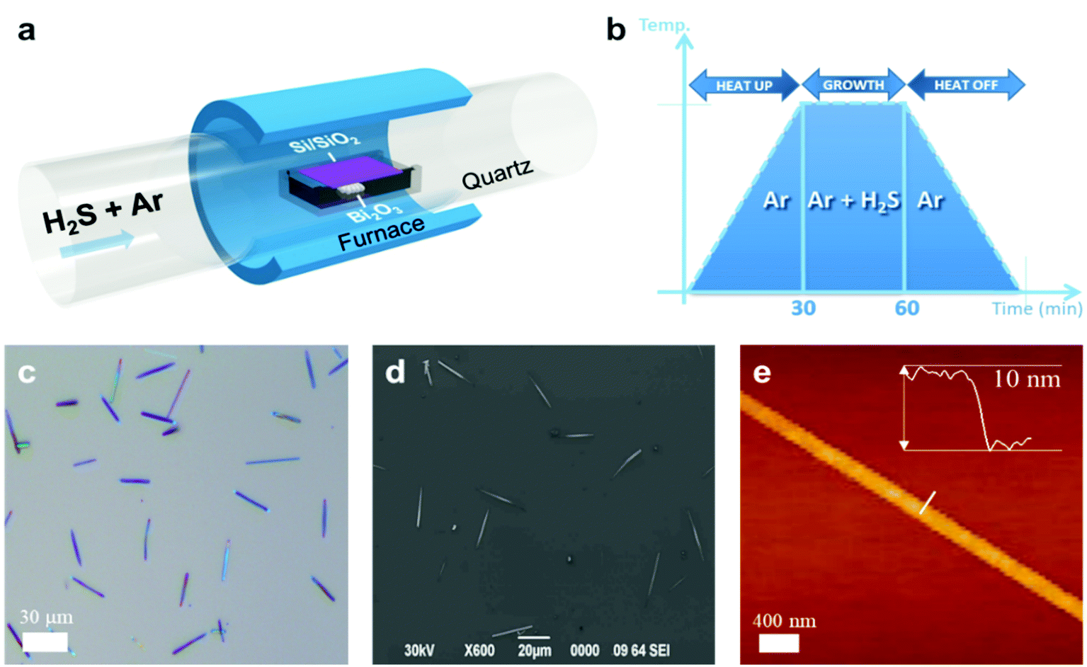 | ||
| Fig. 1 The synthesis method of Bi2S3 and its characterization. (a) Schematic illustration of experimental set-up of Bi2S3, (b) diagram of synthesis process of Bi2S3, (c) OM image of as-grown Bi2S3, (d) SEM image of as-grown Bi2S3, and (e) AFM image and height profile of as-grown Bi2S3. | ||
As depicted in the figure, 2D Bi2S3 multilayer flakes were synthesized in a vacuum quartz tube in a furnace chamber under low pressure (∼10–3 torr). CVD method was carried out using H2S and Bi2O3 powder as precursors and Ar gas was used as a transporting material in whole CVD process. Bi2S3 was directly grown on a SiO2/Si substrate (300 nm SiO2) by sulfurization of Bi2O3 after injection of H2S gas (Fig. 1(a and b)). During the whole growth process, the density and supply duration of H2S gas were exactly adjusted using a mass flow controller and CVD system. While sulfur powder is rapidly vaporised within several min, H2S can provide a rich and steady sulfur environment until the end of the duration of growth. Although Bi2S3 can be synthesized within 10 min, the duration of H2S gas supply increased up to 30 min including annealing process to reduce the sulfur vacancies and improve crystal quality.
2.2. Characterization and structure of Bi2S3
Fig. 1(c) and (d) show optical and electron microscopy images of Bi2S3 multilayer crystals which were grown on the SiO2/Si substrate. The optical microscope image exhibits the contrast of multilayer Bi2S3 with the size of 10–50 micrometers. Also, the shape of synthesized Bi2S3 presents a highly anisotropically structured 1D nanowire. AFM measurements were performed to observe surface states and thicknesses as shown in Fig. 1(e).Fig. 1(e) reveals the highly uniform and clean surface of Bi2S3 crystals without chemical residue and critical defects. The synthesized Bi2S3 samples show a thickness of about 10 nm and a width of about 200 nm.
Raman spectroscopy was used to characterize qualitative physical properties of Bi2S3 samples. As shown in Fig. 2(a), the Raman spectrum was obtained from the sample with approximately 10 nm thickness under a 532 nm wavelength laser and excitation power of 1 mW. The Raman system was calibrated using the Si peak at 520 cm−1. The Raman spectrum shows well-defined main peaks at 185 and 235 cm−1 of Ag phonon mode and 260 cm−1 of B1g phonon mode.32 The Ag and B1g vibration modes are associated with transverse and longitudinal optical phonons respectively. These peak positions match well with those values reported in both of previous theoretical works and experimental results.33 PL spectroscopy was also performed using a 532 nm excitation source. To avoid thermal damage from laser irradiation, 1 mW of power was used for this work. The relatively weak signal of the PL spectrum results from a smaller width of the Bi2S3 sample (∼200 nm) than the spot size of the Raman laser (∼1 μm). As shown in Fig. 2(b), the PL spectrum has the main peak at 917 nm (1.33 eV) which corresponds well to the expected value of the optical band gap.34,35
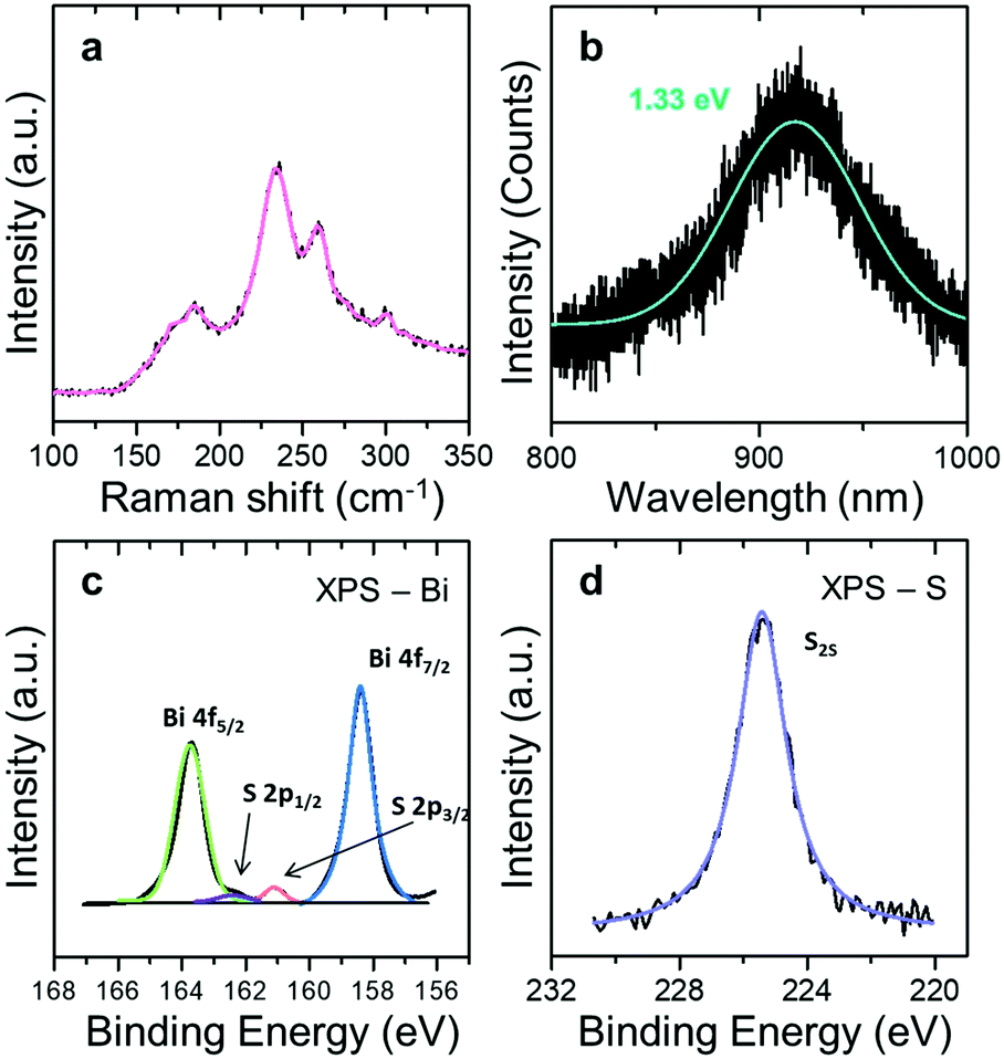 | ||
| Fig. 2 Characterization of optical properties and stoichiometry analysis of Bi2S3 (a) Raman spectrum of Bi2S3, (b) PL spectrum of Bi2S3, (c) XPS spectrum of Bi 4f peaks and S 2p peaks, and (d) XPS spectrum of S 2s peaks. | ||
XPS measurements were carried out to characterize the chemical stoichiometry of the synthesized Bi2S3 crystals and prove low sulfur vacancies of Bi2S3 crystals (Fig. 2(c) and (d)). To obtain exact peak values, the experimental data were fitted with 4 peaks as shown in Fig. 2(c). The 4f spectrum of Bi3+ presents dominant peaks at 163.7 and 158.4 related to 4f5/2 and 4f7/2 respectively.
Similarly, Fig. 2(c) reveals two peaks at 162.3 and 161.1 eV representing S 2p1/2 and S 2p2/3. In Fig. 2(d), the 2s spectrum of S exhibits the peak at 225.3 eV. These results correspond well to the chemical bond between sulfur and bismuth of Bi2S3.33 The Bi 4f orbitals, which result from inherent oxide in Bi2O3 can appear at high binding energy levels.36
The Bi 4f spectrum shows no signal arising from the BixOy radicals or Bi2O3 residues. The atomic ratio of Bi to S is about 0.67 (Fig. 2(c) and (d)), which closely corresponds to the ideal stoichiometry of Bi2S3 and proves the presence of a few sulfur vacancies that result in critical low crystal quality. Furthermore, this result shows lower ratio of sulfur vacancies than CVD-grown Bi2S3 using sulfur powder.37
The electronic band structure of bulk Bi2S3 is plotted in Fig. 3. It displays a semiconducting character with a bandgap of 1.29 eV, in excellent agreement with the previously reported value of 1.3 eV as well as our PL peak value of 1.33 eV.47 The carrier effective mass is calculated by a parabolic fit to the band edge. The hole and electron effective mass from VBM and CBM are 0.39 m0 and 0.25 m0, respectively, where m0 is the free electron mass. Compared with the value of MoS2 (≈ 0.5 m0), such a smaller electron effective mass suggests a comparable or higher electron mobility than that of MoS2 (10–50 cm2 V−1 S−1).48
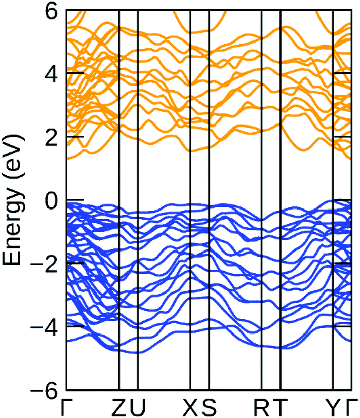 | ||
| Fig. 3 Electronic band structure of bulk Bi2S3. Blue/orange lines for valence/conduction band. The VBM is set to be E = 0. | ||
HR-TEM was used to analyze the crystal structure and evaluate the crystalline quality of a synthesized Bi2S3 sample. The Bi2S3 flakes synthesized on the SiO2/Si substrate were coated with polymethylmethacrylate (PMMA) in a spin-coater. The PMMA coating with the flakes was removed from the substrate in a buffered oxide etchant (BOE) and rinsed in deionized water (DIW) several times.
The PMMA-supported Bi2S3 was transferred onto a TEM copper grid. PMMA was removed in acetone solution and the grid was rinsed in IPA several times. Fig. 4(a) shows the image of HR-TEM of a Bi2S3 flake transferred onto the copper TEM grid. Fig. 4(b) and (c) show the selected area electron diffraction (SAED) pattern and the HR-TEM image of the Bi2S3 flake, respectively. The SAED pattern in Fig. 4(b) presents a periodic orthogonal feature that is associated with a classical anisotropic orthorhombic structure of Bi2S3.
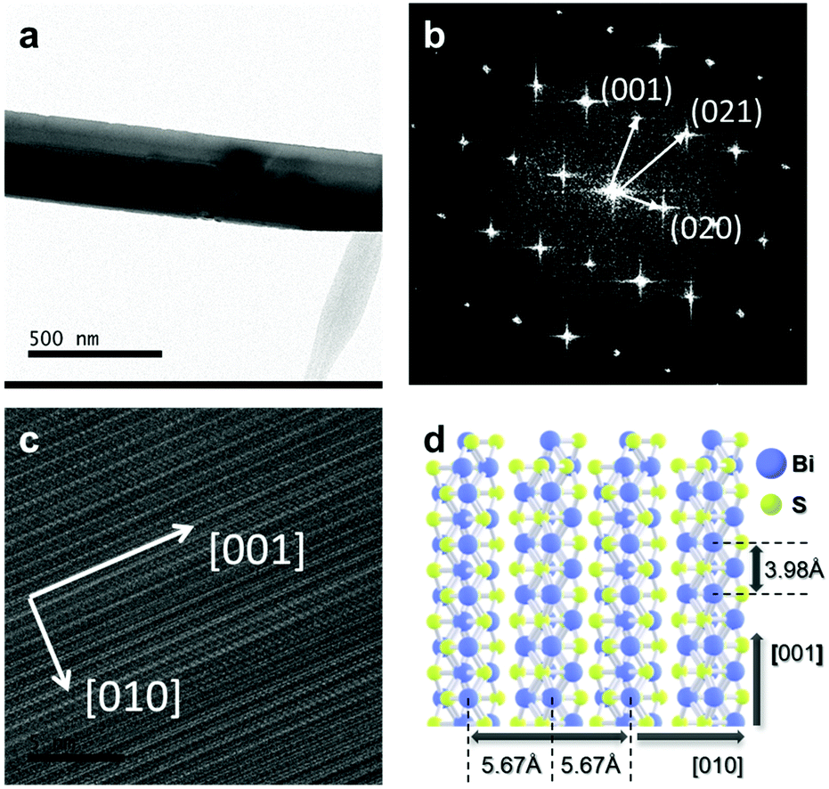 | ||
| Fig. 4 Structure analysis of Bi2S3. (a) TEM image of Bi2S3 on a TEM grid, (b) SAED patterns of single crystalline Bi2S3, (c) HRTEM image of anisotropic Bi2S3 structure, and (d) schematic illustration of Bi2S3 crystal structure. | ||
HR-TEM image shows no impurities and defects in the Bi2S3 crystal. Above all, the SAED pattern reveals a high-quality and perfect single crystal of a synthesized Bi2S3 flake. The diffraction points indicate the lattice planes in the SAED pattern and the (001) plane is perpendicular to the (020) plane.38 This result is in good agreement with the lattice structure of Bi2S3 which is the orthorhombic crystal system with the lattice parameters of a = 0.112 nm, b = 1.125 nm, c = 0.397 nm, α = 90°, β = 90°, γ = 90° as shown in Fig. 4(d).39,40 Also, the low magnification image of HR-TEM in Fig. 4(C) demonstrates the anisotropic growth of Bi2S3 along a main axis of the [001] direction which is perpendicular to the [010] direction due to the anisotropic orthorhombic structure of Bi2S3 (Fig. 4(d)).
2.3. Electrical performance of a Bi2S3 FET
A FET was fabricated to evaluate the electronic properties of the synthesized Bi2S3 sample.In this work, an as-grown multilayer Bi2S3 flake was used for fabrication as shown in Fig. 5(a) and (b). As shown in Fig. 5(a), 5 nm Cr and 50 nm Au as the electrode were deposited using an e-beam evaporator. The gate insulator was made by drop-casting an ionic liquid onto the Bi2S3 flake (Fig. 5(b) and (c)). The ion-gel solution consists of a poly(ethylene glycol) diacrylate (PEG-DA) monomer, a 2-hydroxy-2-methylpropiophenone (HOMPP) initiator, and a 1-ethyl-3-methylimidazolium bis(trifluoromethylsulfonyl)imide (EMIM:TFSI) ionic liquid with a weight ratio of 2:1:22. In Fig. 5(d), the transfer characteristics of the ion-gel gated FETs exhibited n-type behavior, which is consistent with previous reports. The field effect mobility can be calculated using the equation μ = (L/WVDCion-gel) (ΔID/ΔVG), where L, W, and Cion-gel are the channel length, the channel width, and capacitance of the ion-gel gate dielectric.
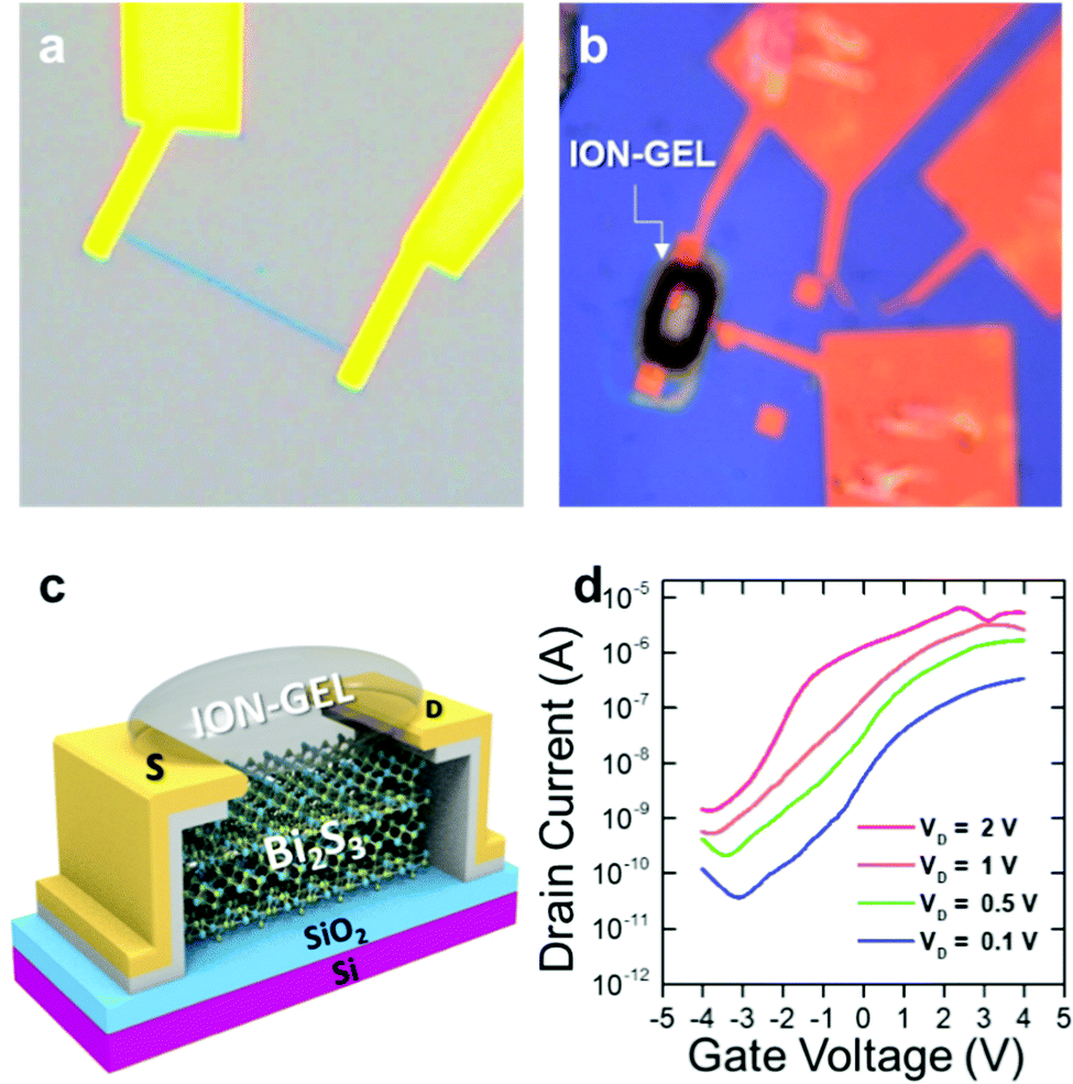 | ||
| Fig. 5 Electronic properties of Bi2S3: (a) OM image of FET based on as-grown Bi2S3, (b) OM image of the ion-gel gated transistor of Bi2S3, (c) schematic diagram of ion-gel gated Bi2S3 FET, (d) transfer characteristics of Bi2S3 transistor. | ||
The value of ΔID/ΔVG was obtained from the slope of the transfer characteristic curve plotted in Fig. 5(d). The FET exhibited a high electron mobility of 100.4 cm2 V−1 S−1, and a high current on/off ratio of ∼104 at VD = 1 V, which are superior to those of other conventional 2D materials such as MoS2, WS2 and ReS2 as well as those of the previously reported Bi2S3 (Table 1). The excellent electronic device performance again proves the high crystallinity of the synthesized flakes and demonstrates the feasibility of practical and high-performance electronic device applications.
3. Experimental
3.1. Synthesis of Bi2S3
Bi2O3 powder (99.9%, Sigma Aldrich) was used as the precursor for the synthesis of Bi2S3. Bi2S3 was grown in a vacuum quartz tube in a furnace under low pressure (∼103 torr). Before synthesis, SiO2/Si (300 nm SiO2) wafer was cleaned in acetone and isopropyl alcohol (IPA) and then rinsed in DIW several times. A mass of Bi2O3 5 mg powder in a quartz boat was put onto the edge of the furnace and covered by SiO2/Si wafer. The furnace was heated up to 550 °C for 30 min and then H2S gas was injected for sulfurization of Bi2O3 for 30 min. The furnace chamber was cooled down to room temperature. Ar gas was injected over the whole process.3.2. Characterization of synthesized Bi2S3
Raman and PL spectroscopy was carried out at 532 nm laser wavelength, and 1 mW laser power, which avoids thermal damage to samples. The Raman instrument (NTMDT AFM-Raman spectroscope) was calibrated using a Si peak of 520 cm−1 before measurement. XPS was performed to determine the chemical stoichiometry and bonding states of Bi2S3 with an Al Kα X-ray source (ESCALAB 220i-XL, VG Scientific Instruments). AFM was used for surface analysis and measurement of the thickness of the samples. AFM measurements (Seiko instrument) were taken with a Si tip (NT-MDT). To make the TEM sample, a Bi2S3 on SiO2/Si wafer was coated with polymethylmethacrylate (PMMA) in a spin-coater. It was immersed in BOE solution to remove SiO2 and then was rinsed in DIW several times. The PMMA-supported Bi2S3 was transferred onto a TEM copper grid and the PMMA was removed in acetone for 30 min and rinsed in IPA several times. The TEM images and SAED patterns were obtained using a JEM-2100F, Cs corrector.3.3. Structure relaxation and electronic band structure calculations
All the DFT calculations were performed using the Vienna ab initio Simulation Package (VASP).49 For the ion–electron interaction, projector augmented wave (PAW) pseudopotentials were used. For the exchange–correlation functional, the Perdew–Burke–Ernzerhof (PBE) type generalized gradient approximation (GGA) was adopted.50 The van der Waals interactions were described by the DFT-D3 Grimme method.51 The Γ-centered k-mesh of 4 × 12 × 5 (9 × 25 × 9) and the plane-wave energy cutoff of 600 eV were set for the structural optimization (electronic band structure calculation). The calculated lattice constants of the relaxed bulk Bi2S3 are a = 11.12 Å, b = 11.29 Å and c = 4.00 Å, in very good agreement with the experimental values (a = 11.2 Å, b = 11.25 Å and c = 3.97 Å).3.4. Device fabrication
A FET based on as-grown Bi2S3 was fabricated using e-beam-lithography. The metal electrodes of Cr/Au (5/50 nm) were deposited by using an e-beam evaporator. To make the gate insulator, the ionic liquid was drop-cast onto the FET. The gate dielectric layer was formed by drop-casting an ion-gel solution comprising poly(ethyleneglycol) diacrylate (PEGDA, Sigma-Aldrich), 2-hydroxy-2-methylpropiophenone (HOMPP, Sigma Aldrich), and 1-ethyl-3-methylimidazolium bis (trifluoromethanesulfonyl) imide ([EMIM][TFSI]) ionic liquid (Merck) in a weight ratio of 2:1:22. After drying, the ion gel layer in a patterned photomask was exposed to UV light (365 nm, 100 mW cm−2) for five seconds. The area exposed to UV light became chemically crosslinked, while the unexposed region was removed by rinsing in DIW.
4. Conclusions
In conclusion, we have developed the CVD method for the synthesis of single crystalline Bi2S3. The crystals have the shapes of 1-dimensional nanowires or nanorods with a width of ∼200 nm and a thickness of tens of nanometers. TEM and SAED patterns revealed anisotropic properties and high crystallinity in the orthorhombic structure of Bi2S3. The optical band gap of Bi2S3 (∼1.33 eV) was confirmed by PL spectroscopy. AFM and SEM images showed clean and uniform surfaces of Bi2S3. Above all, ion-gel gated FETs based on as-grown Bi2S3 displayed superior electronic properties with a charge carrier mobility of 100.4 cm2 V−1 S−1, a current on/off ratio of ∼104 and a low voltage operation below 4 V. The CVD method to grow Bi2S3 single crystals paves a new way for high performance electronics with 2D semiconducting materials.Author contributions
Y. K. developed the synthesis method of Bi2S3 and carried out the analysis of CVD-grown Bi2S3, M. J. conducted the electronic band structure calculation of Bi2S3 and E. J. fabricated the device of Bi2S3 and conducted the electrical test. All authors contributed the discussion and preparation of the manuscript.Conflicts of interest
There are no conflicts to declare.Acknowledgements
This study was supported by the Basic Science Research Program (2021R1F1A1051987, 2016K1A1A2912707, 2018R1A6A3A11047867, 2020R1A2C2014687, and 2019R1I1A1A01061466) through the National Research Foundation of Korea (NRF) and the KISTI grant (KSC-2020-CRE-0325).References
- K. S. Novoselov, A. K. Geim, S. V. Morozov, D.-E. Jiang, Y. Zhang, S. V. Dubonos, I. V. Grigorieva and A. A. Firsov, Science, 2004, 306, 666–669 CrossRef CAS PubMed.
- X. Li, W. Cai, J. An, S. Kim, J. Nah, D. Yang, R. Piner, A. Velamakanni, I. Jung and E. Tutuc, Science, 2009, 324, 1312–1314 CrossRef CAS PubMed.
- K. Watanabe, T. Taniguchi and H. Kanda, Nat. Mater., 2004, 3, 404–409 CrossRef CAS PubMed.
- A. Zunger, A. Katzir and A. Halperin, Phys. Rev. B: Solid State, 1976, 13, 5560 CrossRef CAS.
- C. Lee, H. Yan, L. E. Brus, T. F. Heinz, J. Hone and S. Ryu, ACS Nano, 2010, 4, 2695–2700 CrossRef CAS PubMed.
- V. Podzorov, M. Gershenson, C. Kloc, R. Zeis and E. Bucher, Appl. Phys. Lett., 2004, 84, 3301–3303 CrossRef CAS.
- Y. Chen, J. Xi, D. O. Dumcenco, Z. Liu, K. Suenaga, D. Wang, Z. Shuai, Y.-S. Huang and L. Xie, ACS Nano, 2013, 7, 4610–4616 CrossRef CAS PubMed.
- G.-H. Lee, Y.-J. Yu, X. Cui, N. Petrone, C.-H. Lee, M. S. Choi, D.-Y. Lee, C. Lee, W. J. Yoo and K. Watanabe, ACS Nano, 2013, 7, 7931–7936 CrossRef CAS.
- W. Zhao, Z. Ghorannevis, L. Chu, M. Toh, C. Kloc, P.-H. Tan and G. Eda, ACS Nano, 2013, 7, 791–797 CrossRef CAS.
- J. Qiao, X. Kong, Z.-X. Hu, F. Yang and W. Ji, Nat. Commun., 2014, 5, 1–7 Search PubMed.
- J.-H. Chen, C. Jang, S. Xiao, M. Ishigami and M. S. Fuhrer, Nat. Nanotechnol., 2008, 3, 206–209 CrossRef CAS PubMed.
- F. Xia, V. Perebeinos, Y.-M. Lin, Y. Wu and P. Avouris, Nat. Nanotechnol., 2011, 6, 179–184 CrossRef CAS PubMed.
- A. Allain, J. Kang, K. Banerjee and A. Kis, Nat. Mater., 2015, 14, 1195–1205 CrossRef CAS PubMed.
- A. K. Geim and I. V. Grigorieva, Nature, 2013, 499, 419–425 CrossRef CAS.
- K. Novoselov, O. A. Mishchenko, O. A. Carvalho and A. C. Neto, Science, 2016, 353 Search PubMed.
- K. Keyshar, Y. Gong, G. Ye, G. Brunetto, W. Zhou, D. P. Cole, K. Hackenberg, Y. He, L. Machado and M. Kabbani, Adv. Mater., 2015, 27, 4640–4648 CrossRef CAS.
- C. Ahn, J. Lee, H. U. Kim, H. Bark, M. Jeon, G. H. Ryu, Z. Lee, G. Y. Yeom, K. Kim and J. Jung, Adv. Mater., 2015, 27, 5223–5229 CrossRef CAS PubMed.
- A. M. Hussain, G. A. T. Sevilla, K. R. Rader and M. M. Hussain, International Electronics, Communications and Photonics Conference (SIECPC), 2013, pp. 1–5 Search PubMed.
- H. Liu, A. T. Neal, Z. Zhu, Z. Luo, X. Xu, D. Tománek and P. D. Ye, ACS Nano, 2014, 8, 4033–4041 CrossRef CAS PubMed.
- J.-S. Kim, Y. Liu, W. Zhu, S. Kim, D. Wu, L. Tao, A. Dodabalapur, K. Lai and D. Akinwande, Sci. Rep., 2015, 5, 1–7 Search PubMed.
- K. Biswas, L. D. Zhao and M. G. Kanatzidis, Adv. Energy Mater., 2012, 2, 634–638 CrossRef CAS.
- N. Dhar, N. Syed, M. Mohiuddin, A. Jannat, A. Zavabeti, B. Y. Zhang, R. S. Datta, P. Atkin, N. Mahmood and D. Esrafilzadeh, ACS Appl. Mater. Interfaces, 2018, 10, 42603–42611 CrossRef CAS PubMed.
- D. J. Riley, J. P. Waggett and K. U. Wijayantha, J. Mater. Chem., 2004, 14, 704–708 RSC.
- R. Vogel, P. Hoyer and H. Weller, J. Phys. Chem., 2002, 98, 3183–3188 CrossRef.
- Z. Zhang, W. Wang, L. Wang and S. Sun, ACS Appl. Mater. Interfaces, 2012, 4, 593–597 CrossRef CAS PubMed.
- B. Chen, C. Uher, L. Iordanidis and M. G. Kanatzidis, Chem. Mater., 1997, 9, 1655–1658 CrossRef CAS.
- F. Wald, J. Bullitt and R. Bell, IEEE Trans. Nucl. Sci., 1975, 22, 246–250 Search PubMed.
- K. Yao, Z. Zhang, X. Liang, Q. Chen, L.-M. Peng and Y. Yu, J. Phys. Chem. B, 2006, 110, 21408–21411 CrossRef CAS PubMed.
- K. A. Messalea, A. Zavabeti, M. Mohiuddin, N. Syed, A. Jannat, P. Atkin, T. Ahmed, S. Walia, C. F. McConville and K. Kalantar-Zadeh, Adv. Mater. Interfaces, 2020, 7, 2001131 CrossRef CAS.
- M. Xie, J. Zhou, H. Ji, Y. Ye, X. Wang, K. Jiang, L. Shang, Z. Hu and J. Chu, Appl. Phys. Lett., 2019, 115, 121901 CrossRef.
- T. Yanase, F. Uehara, I. Naito, T. Nagahama and T. Shimada, ACS Appl. Nano Mater., 2020, 3, 10462–10469 CrossRef CAS.
- I. Zumeta-Dube, J.-L. Ortiz-Quiñonez, D. Díaz, C. Trallero-Giner and V.-F. Ruiz-Ruiz, J. Phys. Chem. C, 2014, 118, 30244–30252 CrossRef CAS.
- J. Grigas, E. Talik and V. Lazauskas, Phys. Status Solidi B, 2002, 232, 220–230 CrossRef CAS.
- X. Yu, C. Cao and H. Zhu, Solid State Commun., 2005, 134, 239–243 CrossRef CAS.
- Y. Zhao, K. T. E. Chua, C. K. Gan, J. Zhang, B. Peng, Z. Peng and Q. Xiong, Phys. Rev. B: Condens. Matter Mater. Phys., 2011, 84, 205330 CrossRef.
- Z. Bian, J. Zhu, S. Wang, Y. Cao, X. Qian and H. Li, J. Phys. Chem. C, 2008, 112, 6258–6262 CrossRef CAS.
- J. Xu, H. Li, S. Fang, K. Jiang, H. Yao, F. Fang, F. Chen, Y. Wang and Y. Shi, J. Mater. Chem. C, 2020, 8, 2102–2108 RSC.
- M. B. Sigman and B. A. Korgel, Chem. Mater., 2005, 17, 1655–1660 CrossRef CAS.
- Y. Li, L. Huang, B. Li, X. Wang, Z. Zhou, J. Li and Z. Wei, ACS Nano, 2016, 10, 8938–8946 CrossRef CAS PubMed.
- G. Chen, Y. Yu, K. Zheng, T. Ding, W. Wang, Y. Jiang and Q. Yang, Small, 2015, 11, 2848–2855 CrossRef CAS PubMed.
- A. M. Van Der Zande, P. Y. Huang, D. A. Chenet, T. C. Berkelbach, Y. You, G.-H. Lee, T. F. Heinz, D. R. Reichman, D. A. Muller and J. C. Hone, Nat. Mater., 2013, 12, 554–561 CrossRef CAS PubMed.
- F. Reale, P. Palczynski, I. Amit, G. F. Jones, J. D. Mehew, A. Bacon, N. Ni, P. C. Sherrell, S. Agnoli and M. F. Craciun, Sci. Rep., 2017, 7, 1–10 CrossRef CAS PubMed.
- X. He, F. Liu, P. Hu, W. Fu, X. Wang, Q. Zeng, W. Zhao and Z. Liu, Small, 2015, 11, 5423–5429 CrossRef CAS PubMed.
- K. Keyshar, Y. Gong, G. Ye, G. Brunetto, W. Zhou, D. P. Cole, K. Hackenberg, Y. He, L. Machado and M. Kabbani, Adv. Mater., 2015, 27, 4640–4648 CrossRef CAS PubMed.
- F. Lu, R. Li, Y. Li, N. Huo, J. Yang, Y. Li, B. Li, S. Yang, Z. Wei and J. Li, ChemPhysChem, 2015, 16, 99–103 CrossRef CAS PubMed.
- K. A. Messalea, A. Zavabeti, M. Mohiuddin, N. Syed, A. Jannat, P. Atkin, T. Ahmed, S. Walia, C. F. McConville and K. Kalantar-Zadeh, Adv. Mater. Interfaces, 2020, 7, 2001131 CrossRef CAS.
- I. Efthimiopoulos, J. Kemichick, X. Zhou, S. V. Khare, D. Ikuta and Y. Wang, J. Phys. Chem. A, 2014, 118, 1713–1720 CrossRef CAS PubMed.
- A. Rawat, N. Jena and A. De Sarkar, J. Mater. Chem. A, 2018, 6, 8693–8704 RSC.
- G. Kresse and J. Furthmüller, Comput. Mater. Sci., 1996, 6, 15–50 CrossRef CAS.
- J. P. Perdew, K. Burke and M. Ernzerhof, Phys. Rev. Lett., 1996, 77, 3865 CrossRef CAS PubMed.
- S. Grimme, J. Antony, S. Ehrlich and H. Krieg, J. Chem. Phys., 2010, 132, 154104 CrossRef PubMed.
| This journal is © the Owner Societies 2021 |