
Exploring the emerging of electronic and magnetic properties with adatom adsorption on a novel semiconductor monolayer: N2P6†
Xinle
Lu
 ab,
Liaoxin
Sun
b,
Bing
Fu
c,
Shoutian
Sun
*a and
Xiang
Ye
*a
ab,
Liaoxin
Sun
b,
Bing
Fu
c,
Shoutian
Sun
*a and
Xiang
Ye
*a
aDepartment of Physics, Shanghai Normal University, Shanghai 200234, P. R. China. E-mail: stsun@shnu.edu.cn; yexiang@shnu.edu.cn
bState Key Laboratory of Infrared Physics, Chinese Academy of Sciences, Shanghai 200083, P. R. China
cFuzhou Medical College of Nanchang University, Fuzhou 344000, P. R. China
First published on 7th September 2021
Abstract
The effect of adsorbed adatoms on the structural stability and electronic properties of monolayer N2P6 have been systematically studied via first-principles simulation methods. It is found that pristine N2P6 is an indirect 0.21 eV band gap semiconductor, with a pleated honeycomb-like structure similar to phosphorene. The calculation results show that adsorbed adatoms can modify the properties of monolayer N2P6 effectively. The degree of local distortion strongly depends on the electronegativity and size of adatoms, also the adsorption energy ranges from 0.3 to 5.8 eV depending on the species of adatoms. The electronic properties show metallic behavior with several adsorbed metal atoms (Li, Na, Al, K, Cu, Ni, and Zn) and some non-metal atoms (H, F, P, and Cl), while adsorbed O, S, Ca, and Si atoms still remain semiconductors. The systems of Ni and Zn adatoms show ferromagnetic behavior, and adsorbed Mg exhibits a half-metallic character. Our theoretical studies indicate that N2P6 possesses potential application in the field of gas sensors.
1. Introduction
Research on low-dimensional materials has entered an unprecedented boom since graphene was first exfoliated mechanically from three-dimensional (3D) graphite in 2004.1 In recent years, inspired by the finding of graphene, more and more two-dimensional (2D) materials have been found and explored, such as transition–metal dichalcogenides (TMDCs),2 transition metal oxide silicene, graphene-like two-dimensional materials,3 MXenes,4,5etc. These 2D materials possess unique electrical, optical, magnetic and mechanical properties.6–9 In addition, an important advantage of these materials is that it is easier to regulate their electronic and magnetic properties than those of the bulk using various approaches, for example, embedding of atoms,10 electric-field effect,11 defect engineering, strain engineering,12 adsorbing functional groups13,14 and so on.9Graphene, as a single-layer honeycomb lattice of carbon atoms, has been widely used in various applications including solar cells,15 electrodes,16 wearable devices,17 and sensors,18,19 owing to its high transparency, high thermal conductivity and high specific surface area. However, the zero bandgap of graphene20 with a smaller switching current ratio prohibits its applications as a logic switch in semiconductors. Several graphene-like materials3,21 and their allotropes have been synthesized experimentally. It has been found that defects and adsorption of adatoms on top of graphene-like C2N, C3N, C3N4, and C4N3 can modify their electrical and magnetic properties, which could be useful for application in gas sensors.22–25
Although a 2D transition metal sulfide (such as MoS22) has a high current switching ratio, its carrier mobility is much lower than that of graphene, which limits the application of transition metal sulfides in electronics.26 In 2014, phosphorene was successfully exfoliated from the bulk black phosphorus (BP) phase using mechanical exfoliation.27 It is a direct semiconductor with excellent electrochemical performance. And as an electrode material, phosphorene has an ultra-high specific capacity of 2596 mA h g−1 in lithium-ion batteries, which is much higher than that of graphite.28,29 Owing to phosphorene's “puckered” honeycomb structure, it possesses a much higher surface to volume ratio and lower out-of-plane electrical conductance, while its chemical stability is lower than those of graphene and TMDCs.30 Adsorption of gas molecules on phosphorene has been extensively investigated and it has been demonstrated that phosphorene could be a superior gas sensor.31,32 Abbas et al. found that the phosphorene based FET sensors have excellent sensitivity to 5 ppb NO2.33 In particular, researchers have recently shown the superior selectivity of green phosphorene towards the decomposition of numerous SF6 gases.34 However, black phosphorene can only show strong physical adsorption to nitrogen-containing gas molecules, such as NO, NO2 and NH3, which inhibits its application for gas detection. Subsequently, more efforts have been made to improve the adsorption ability of black phosphorene, including surface decoration.25,35 In addition, binary phosphorus nitrides show potential in electronic devices and optoelectronics, drawing the attention of researchers. Ma et al. predicted three 2D phosphorous nitride (PN) single-layer sheets (named α-, β- and γ-PN) with superior mobility based on first-principles methods.36 Dong et al. designed three 2D materials (named P2N2, P3N and δ-P3B) exhibiting extraordinary stability. Among them, P3N with 3% strain could become a good photocatalyst for water splitting.37 What's more, most 2D materials of group V elements were synthesized at high pressure and high temperature, such as the BP allotrope of nitrogen (bp-N), α-P3N5 and γ-P3N5, have excellent thermal, mechanical and chemical stability.38,39
Thus, based on the excellent properties of phosphorene in gas sensing and the structural stability of binary phosphorus nitrides, we have predicted a kind of nitrogen and phosphorus compound N2P6. Electronic properties and crystal orbital Hamilton population (COHP) were studied via density functional theory (DFT) calculations.40–43 Pristine N2P6 is a pleated honeycomb-like 2D semiconductor with an indirect band gap of 0.21 eV. The adsorption of 22 different atoms including alkali metal (Li, Na, and K), alkaline earth metal (Be, Mg, and Ca), and 3d transition-metal (Fe, Co, Ni, Cu, and Zn) elements, and nonmetallic atoms (H, B, C, N, O, F, Si, P, S and Cl) and Al on N2P6 have been studied. It is found that some adatoms (B, Be, C, N, Fe, and Co) modify the geometry of the substrate, and other adatoms can become adsorbed at four stable adsorption sites of N2P6, except Li and Zn adatoms that show a small deviation from the special adsorption sites. The results also show that H, Na, Mg, Al, K and Ca prefer to stay on the top of N atom of N2P6, while non-metallic adatoms O, F, S and Cl prefer to stay on the top of P atom. Other atoms are adsorbed on the top of the P6 ring (Si, Ni and Cu) and the P–P bridge (P) site. The electronic properties reveal that different species of adatoms can modulate the bandgap of the system effectively which could give rise to the donor and acceptor states. Even Ni and Zn adatoms make N2P6 attain its magnetic properties. Furthermore, Ken et al. verified the formation of new PxNy monolayers by laser heating under 67 and 70 GPa pressure, which indicates the possibility of synthesis of the N2P6 monolayer in the future.44 We believe that our results will help to understand the properties of adsorption N2P6 and promote its application in the field of gas sensors.
2. Methods
The particle swarm optimization (PSO) method implemented in the CALYPSO45,46 code is employed to locate the stable structures of 2D nitrogen and phosphorus compounds. To ensure convergence, the numbers of generation and population size are set to be 30. And for better querying of the configurations, 1 to 4 formula units in each unit cell are used. The density functional theory calculations47 were performed using the generalized gradient approximation for the exchange–correlation functional as proposed by Perdew–Burke–Ernzerhof (GGA–PBE) in VASP.48,49 The energy cutoff was set to be 600 eV. The energy and force convergence criteria for the structure optimization were set to be 1 × 10⁻⁷ eV per supercell and 0.02 eV Å−1, respectively. A k-point mesh of 5 × 5 × 1 was generated using Monkhorst–Pack scheme50 for geometry optimization and a 9 × 9 × 1 mesh was used for electronic properties calculations. A vacuum region of about 20 Å was applied in the z-direction. Furthermore, we explored a periodic 2 × 2 × 1 supercell N2P6 as the substrate. Bader charge analysis was used to calculate charge transfer51 for electronic analysis. To investigate the chemical-bonding, LOBSTER is used to calculate and visualize the bonding and antibonding contributions.52,533. Results and discussions
3.1 Pristine N2P6
The most stable structure predicted using the PSO method is found to be the 2D N2P6 monolayer. The optimized buckle structure of the pristine N2P6 monolayer is shown in Fig. 1(a). The lattice constants are a = b = 6.036 Å and the thickness along the z-direction is around 1.338 Å. The unit cell consists of two N and six P atoms, and the P6 rings are connected with each other by N atoms. The optimized bond distances for N–P, P–P are 1.797 and 2.273 Å, respectively. The P–P–P bond angle in the six-membered ring is ∼88.89°. Based on this structure, the phonon spectra and first principles molecular dynamics (FPMD) simulations are adopted to inspect dynamic and thermal stability, respectively. The phonon spectra show small negative values in the Γ region, which is caused by a defect in the algorithm.37,54 So, N2P6 could be considered to be dynamically stable. Through FPMD simulations on pristine N2P6 at 300 K, we found that the total energy is nearly fluctuating around a constant value throughout the simulation and after 3000 steps there are no substantial deformations in N2P6 as shown in Fig. S1 (ESI†).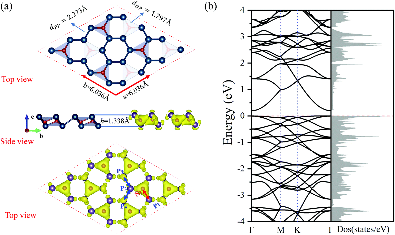 | ||
| Fig. 1 (a) The top and side view of optimized structure, total charge density of N2P6 monolayer. Rufous (cyan), or red (brown) dots are N (P) atoms. (b) The band structure and density of states (DOS) of N2P6 corresponding to the left structure. | ||
Due to the different electronegativities (N: 3.04; P: 2.19), a charge transfer occurs from P to N atoms. As seen in Fig. 1(a), there is a higher charge density around N atoms compared to P atoms. Each N atom obtains about 1.74 electrons from its neighbor P atoms according to Bader charge analysis, which is consistent with the electronegativity model and charge density difference as shown in Fig. S2 (ESI†). According to our results, the P atoms are positively charged, whereas the N atoms are negatively charged, resulting in a strong bonding character of N–P bonds. Moreover, the total charge density revealed that spatial configuration of N atoms is tetrahedral, verifying that it is the sp3 nonequivalent hybridization of N and P atoms, which induces the folded two-dimensional honeycomb-like structure.
The projected band structure of N2P6 is shown in Fig. 2. The results show that the N2P6 is an indirect semiconductor (bandgap: 0.21 eV), with the valence band maximum (VBM) and the conduction band minimum (CBM) located at M and Γ points, respectively. It can be seen that the VBM is predominantly contributed by the pz orbitals of N and P atoms, while the CBM is mainly composed of the pz orbital of P atoms. For elements of group V monolayers or binary phosphorus nitrides (P3N5), the PBE_GGA functionals commonly underestimate the size of the bandgap.55 Hence, we adopted Heyd–Scuseria–Ernzerhof (HSE06) exchange–correlation functionals to predict reliable electronic structures. The estimated band gap is 1.05 eV as shown in Fig. S3 (ESI†).
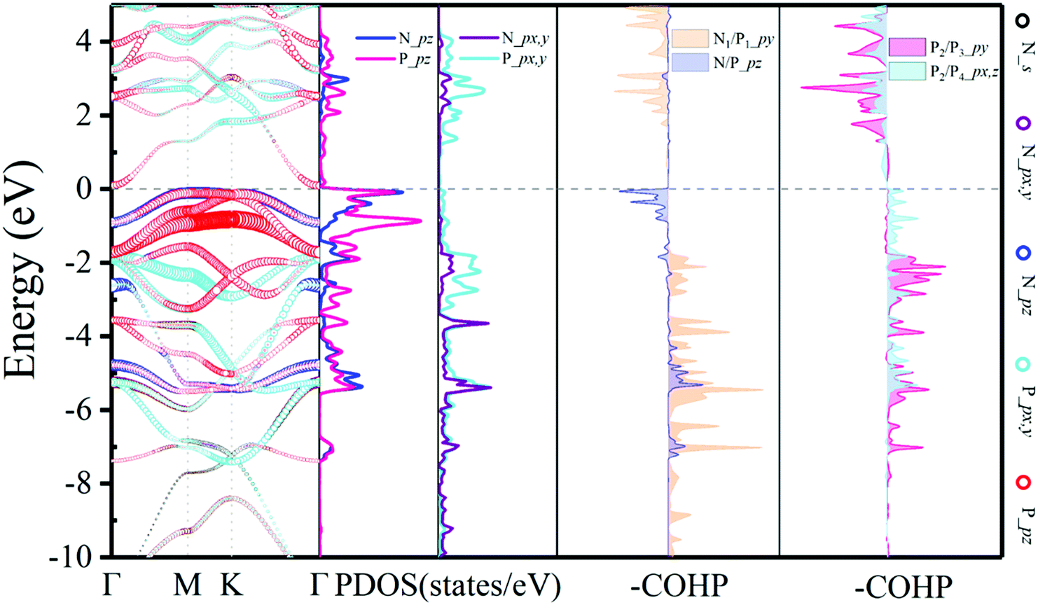 | ||
| Fig. 2 Electronic structure with orbital resolved band structure, the corresponding PDOS and –COHP results of the N2P6 unit cell. The Ef is set to zero as shown by the dashed line. | ||
To achieve an in-depth understanding of this structure, the partial density of states (PDOS) and the COHP have been calculated and analyzed. The PDOS and –COHP are depicted in Fig. 2, confirming that this structure is relatively stable and could be synthesized experimentally. Notice that N_pz and P_pz dominate in the PDOS around the Fermi level; thus we focus on –COHP of N–P and P–P bonds to analyze the bonding character. The coupling of N/P_px,y,z orbitals are the main source in the formation of covalent N–P bonds. For optimized N2P6, there is three-fold rotational symmetry Ĉ3 at the position of the N atom, and all of the coupling between N and P is exactly the same. Thus, a typical N1–P1 (red arrow in Fig. 1a) bond was selected to perform COHP analysis. As the -COHP images in Fig. 2 show, the N/P_pz interaction (ondine area) produce part of anti-bonding components below the Fermi energy, and almost of the occupied states are bonding components for the coupling of N/P_py (pale orange area). Two different P–P bonds are observed (blue arrow in Fig. 1a), one (P2–P3), perpendicular to a-axis, is that P/P_py (rose area) interaction which is stronger than other orbitals; other P–P bonds (P2–P4) intensities mainly come from the px, pz orbital coupling. Their –COHP indicates that the bonding of these two kinds of P–P is stable. On the other hand, the N–P (ICOHP: Integral Crystal orbital Hamilton population = −3) bonding strength is stronger than the P–P (ICOHP = −2.3) one. The strong interaction between N_pz and P_pz induces splitting of the energy band near the Fermi level.
3.2 Adsorption of adatoms on N2P6
Adsorption of adatoms will modify the structural, electronic, and magnetic properties of the N2P6 monolayer. Totally 21 different adatoms on N2P6 have been studied. The possible adsorption geometries are predicted using Calypso with the most stable structures shown in Fig. 3. In general, four different configurations have been identified, including (1) the top site above a N atom (TN): H, Al, Mg, K, and Ca; (2) the top site above a P atom (TP): O, F, S, and Cl; (3) the hollow site above the center of a hexagon with six P atoms (HPP): Si, Ni, and Cu; and (4) the bridge site above the middle of a P and the next neighbor P (BPP): P. Li, and Zn adatoms are always relaxed to non-special points deviated from the special adsorption sites (Fig. 10(b)). In brief, adatom-N2P6 (Al–N2P6) represents the entire system after the substrate has adsorbed the adatom (Al).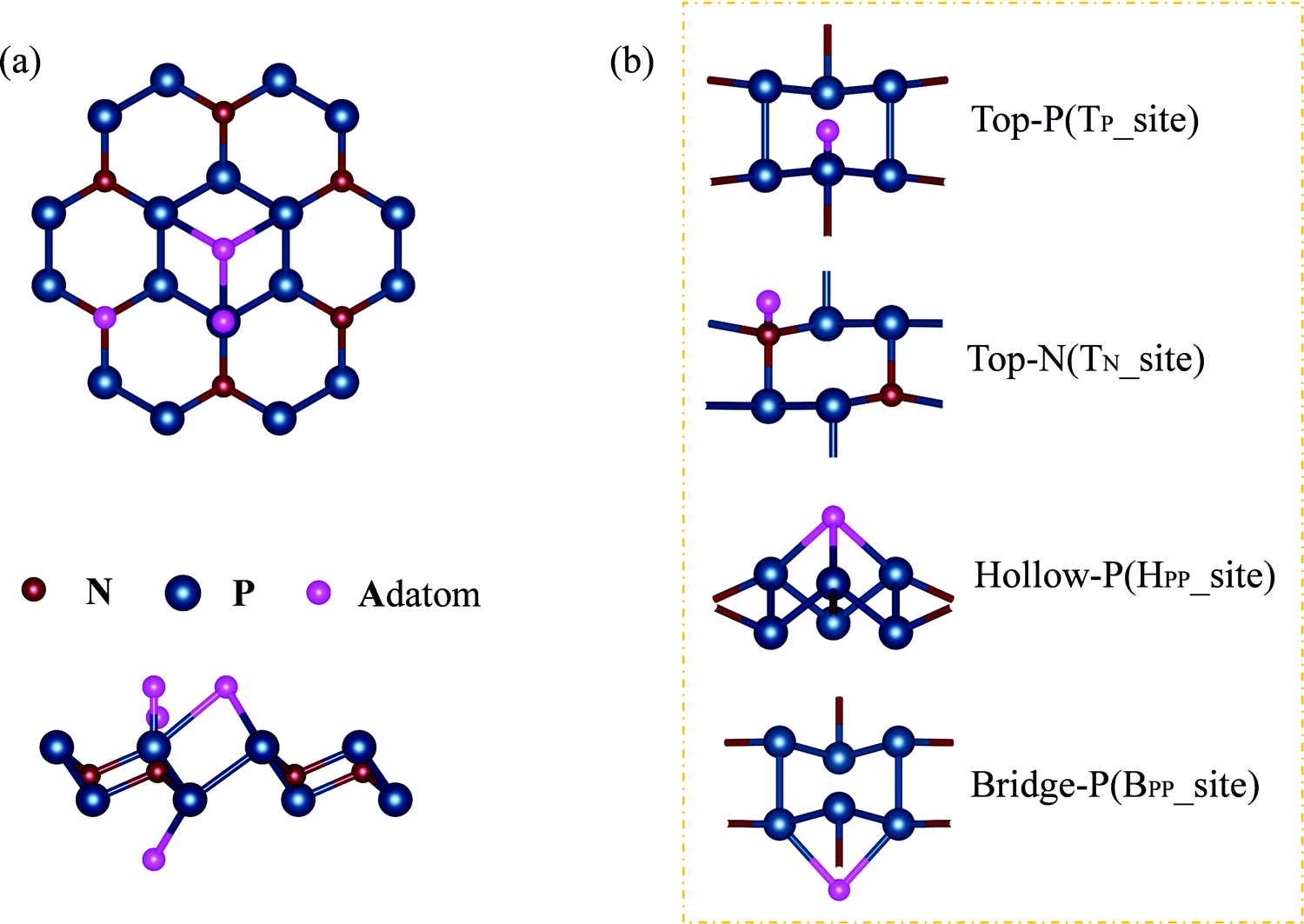 | ||
| Fig. 3 (a) A schematic illustration of top and side views of the embedded single atom, and (b) adsorption sites of the atoms on monolayer N2P6 as presented in Table 1. | ||
Notice that adsorbed B, Be, Co, Fe, and N atoms on N2P6 break the substrate structure due to the strong interaction between adatoms and N2P6. For other systems, we calculated the ICOHP value of the system and found the results to be negative as shown in Table 2. This indicates that all bonds are stable as ICOHP values for all of the N–P, P–P bonds in the adsorption system, approximately the same as that of pristine N2P6. Hence, the Ad–N2P6 systems are stable. We used the biggest change (Δl = |lp–p − lp–p(sub0)|, lp–p(sub0) = 3.183 Å) of the distance (lp–p) between the P atom and its third nearest atom to describe the in-plane local distortion, and out-plane buckling of N2P6 is defined by the height change (Δh = |h − hsub0|, hsub0 = 1.338 Å, hsub0 is the height of pristine N2P6) when compared against pristine N2P6. Fig. 4 shows the tendency of charge transfer (CT) and distortion magnitude (Q) which is described by in-plane distortion Δl and out-plane distortion Δh, that is  (Fig. 4(b)).
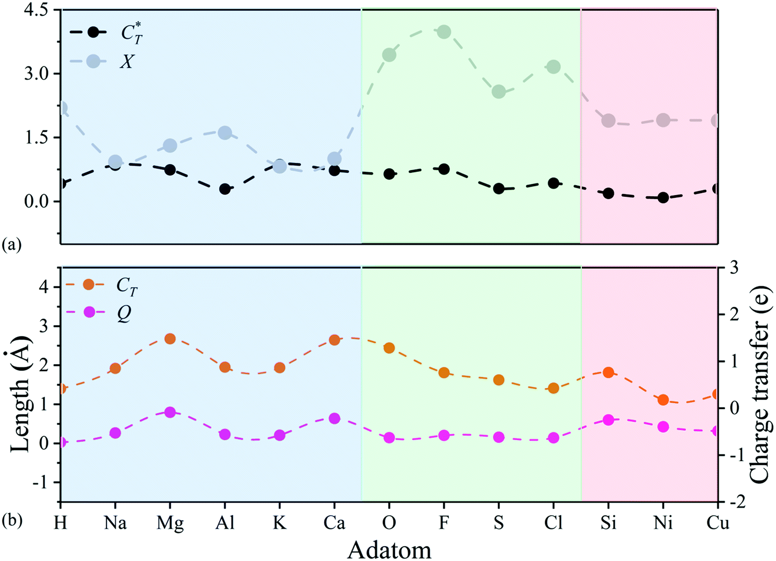 | ||
Fig. 4 (a) Charge transfer capability ( , dashed black curve) and electronegativity (X, dashed grey curve) for different adatoms. (b) Comparison between the distortion magnitude of N2P6 structure (Q, dashed rose curve) and the charge transfer of adatoms (CT, dashed orange curve). The adsorption type of TN, TP, HPP are represented by light blue, green and red area, respectively. , dashed black curve) and electronegativity (X, dashed grey curve) for different adatoms. (b) Comparison between the distortion magnitude of N2P6 structure (Q, dashed rose curve) and the charge transfer of adatoms (CT, dashed orange curve). The adsorption type of TN, TP, HPP are represented by light blue, green and red area, respectively. | ||
The results show tendency to have high consistency in structural distortion and charge transfer of adatoms. To better understand the structural distortion, we analyze the variation of structural parameters, including bond length, height, bond angle and buckling for different adatoms adsorbed N2P6 (Fig. S4, ESI†). Adsorptions on the TN and HPP site mainly exhibit in-plane distortion and have similar degree of in-plane and out-of-plane distortion to CT, which further verifies the relevance between charge transfer and distortion. As for the TP site, there are small changes in the distortion magnitude. Hence, the variation of the relative angle (Δθ = θ − θ0, θ0 = 88.89°) for each system has been studied, which is defined as the maximum variation of the angle θ made up by adatoms nearest the P atom and its first and second P–P bond, and we found that adsorption behavior mainly cause alteration of N/P atomic position (bottom panel of Fig. S4, ESI†). However, focusing on the area closest to the adsorbed atom, adatoms have more impact on dNP and dPP at TP sites than TN and TPP sites. This indicates that the distortion by TP adsorption is more localized than other adsorption sites. The length of N–P bonds is smaller than the substrate while the P–P bond is longer at the stable TN site (light blue area), the main reason being the charge transfer between the N and adatoms elongates N–P bond length. Similarly, the length of N–P, P–P bonds decreased on TP, HPP sites (light green, light red area), and adsorbed O, F, S, and Cl atoms mainly cause out plane bulking, but retain the atomic structure to a great extent compared to TN, HPP adsorption sites as shown in the top panel of Fig. S4 (ESI†).
Then, we defined a physical quantity, charge transfer capability 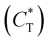 which is obtained by the charge transfer value and the maximum electron number the adatom can gain or lose, to verify the accuracy of charge transfer (Take the H atom as an example; it can lose at most one electron, if the actual charge given is 0.418, the value of
  . Similarly, there is 2e located in the outermost orbit of Mg atom, if the actual charge given is 1.483, then we could get
  ) and use it to compare electronegativities. For TN and HPP adsorption sites, the curve trend of charge transfer capability shows the opposite behavior of electronegativity due to adatom electronegativity being lower than those of N/P atoms (3.04/2.19). And the trend of charge transfer capability is similar to the electronegativity for TP site adsorption. Obviously, it proves that the charge transfer is dominated by electronegativity. In general, the extent of structural distortion depends on the electronegativity of adatoms. The adsorption energy is defined as Ea = EAd/N2P6 − EAd − EN2P6, where EAd/N2P6 is the total energy of the structure with adatom adsorption on N2P6, EN2P6 is the total energy of pristine N2P6, and EAd is the total energy of an isolated adatom in a vacuum (Table 1). The calculation results show that adsorbed atom systems are stable (Ea < 0). The adsorption energies of adatoms located at the stable TN, TP, HPP, and BPP sites ranges from −5.9 to −1.9 eV, which can be considered as chemisorption.
| Adatom | Site | d TC | d NP | d PP | h | θ | l P–P | C T | E a (eV) | E g (eV) | M (μB) |
|---|---|---|---|---|---|---|---|---|---|---|---|
| Al | TN | 2.095 | 1.852 | 2.262 | 1.559 | 84.683° | 3.124 | −0.877 | −2.962 | M | 0 |
| Mg | TN | 2.076 | 1.859 | 2.250 | 2.085 | 80.490° | 2.910 | −1.482 | −1.929 | HM | 0 |
| H | TN | 1.039 | 1.885 | 2.253 | 1.342 | 90.947° | 3.212 | −0.418 | −2.664 | M | 0 |
| Ca | TN | 2.293 | 1.844 | 2.250 | 1.943 | 82.794° | 2.978 | −1.456 | −2.959 | 0.21 | 0 |
| Na | TN | 2.366 | 1.823 | 2.259 | 1.595 | 86.872° | 3.104 | −0.851 | −2.648 | M | 0 |
| K | TN | 2.799 | 1.859 | 2.259 | 1.540 | 87.684° | 3.130 | −0.866 | −4.086 | M | 0 |
| Cl | TP | 2.066 | 1.671 | 2.207 | 1.373 | 97.570° | 3.321 | 0.428 | −2.547 | M | 0 |
| S | TP | 1.951 | 1.728 | 2.249 | 1.438 | 94.542° | 3.304 | 0.603 | −3.602 | 0.304 | 0 |
| O | TP | 1.496 | 1.716 | 2.248 | 1.384 | 95.241° | 3.321 | 1.286 | −5.852 | 0.259 | 0 |
| F | TP | 1.608 | 1.653 | 2.200 | 1.428 | 99.821° | 3.366 | 0.603 | −4.347 | M | 0 |
| Cu | HPP | 2.309 | 1.763 | 2.254 | 1.632 | 94.208° | 3.057 | −0.300 | −2.858 | M | 0 |
| Si | HPP | 2.419 | 1.757 | 2.223 | 1.868 | 101.10° | 2.899 | −0.763 | −3.778 | 0.265 | 0 |
| Ni | HPP | 2.183 | 1.777 | 2.264 | 1.704 | 95.342° | 2.965 | −0.178 | −4.187 | M | 0.590 |
| P | BPP | 2.185 | 1.715 | 2.248 | 2.169 | 74.583° | 2.737 | −0.036 | −2.992 | M | 0 |
| Li | 2.036 | 1.845 | 2.256 | 1.603 | 88.885° | 3.160 | −0.883 | −3.071 | M | 0 | |
| Zn | 2.266 | 1.842 | 2.248 | 1.576 | 86.929° | 3.085 | −0.544 | −0.344 | M | 0.494 |
The structural, electronic, and magnetic parameters of adsorption structures involving TN, TP, HPP and BPP adsorption sites are listed in Table 1. This includes the bond length between adatom and its nearest atom (dTC), the bond length of N–P atoms (dNP), the bond length of P–P atoms (dPP), the height of adsorption structure, the charge transfer (CT) between the embedded atom and N2P6 monolayer, the adsorption energy of adatom (Ea), and magnetic parameters are measured by the magnetic moment per supercell (μ). An electronic state is specified as metal (M), half-metal (HM), or semiconductor (SC), and correspond to the band gap of the adsorption system (Eg).
3.3 Electronic and magnetic properties
The effects of adsorbed adatoms on the electronic and magnetic properties of N2P6 are studied by calculating –COHP,56 fatband structure, DOS, PDOS, and Bader charge. For the band structure, we use the HSE06 functional which chooses 25% short-range exchange using the Hartree–Fock exact exchange, with 2 × 2 × 1 of the k-point sampling, to calculate the electronic structure of two kinds of adsorption systems. Compared with HSE06, PBE functional does underestimate the bandgap, but the band dispersions remain virtually unchanged, and the qualitative results by both PBE and HSE06 are similar. The comparison of PBE and HSE06 is shown in Fig. S3 (ESI†). So, all the calculations were carried out using PBE in this work due to the limiting computational resources. At first, we consider adsorbed atom systems of which the adatoms (H, Na, Mg, Al, K, and Ca) are located at TN site. The adsorption energies of adatoms are in the range of −4.086 to −1.9 eV. dTC ranges from 1.039 to 2.798 Å, which coincides with the value of chemical bond between adatoms and N atoms. Therefore, H, Na, Mg, Al, K and Ca show chemical adsorption. The interaction between adatoms and substrate will cause charge transfer. The amount of charge transfer is denoted as CT with “−” and “+” denoted for giving and gaining electrons, respectively. For adatoms at the stable TN site, adatoms are easier to give electrons to its nearest N atom due to the low electronegativity (0.82–2.2). To further investigate the mechanism between adatoms and their nearest N atoms, the –COHP of adsorption system and integral COHP (ICOHP) values are calculated, which are shown in Fig. 5 and Table 2, respectively. The ICOHP values are very small, suggesting that chemical bond between metal adatoms (Mg, Na, Ca, and K) and their nearest N atoms is owing to the weak bonding strengths, so they are ionic bonds. The corresponding –COHP of Li and Na adsorption system implies that the bond between Ad_s and N_pz is the decisive factor for the strength of the Ad/N bond. –COHP of Li and Na shows that the bonding state is below the Fermi level, and above the Fermi level is the anti-bonding state, suggesting that the adsorption system is stable. But ICOHP value of Al adsorption is not small and the corresponding –COHP shows anti-bonding exists below the Fermi level, which implies that the bond of Al_N may not be ionic.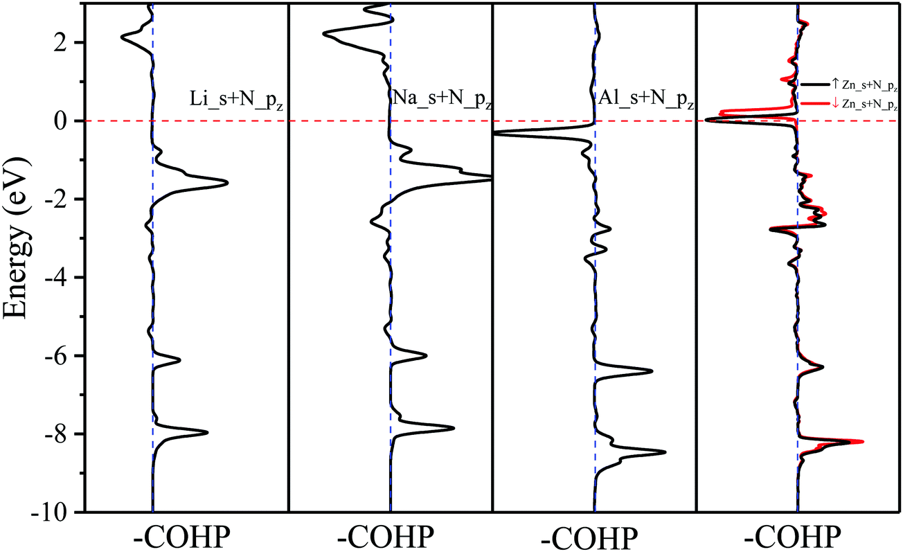 | ||
| Fig. 5 –COHP analysis of metal atoms (Li, Na, Al, and Zn) adsorbed on N2P6. | ||
| Adatom | ICOHP | Adatom | ICOHP | |
|---|---|---|---|---|
| TN | H–N | −3.56789 | Al–N | −1.51874 |
| Mg–N | −0.25946 | Ca–N | −0.21766 | |
| Na–N | −0.18104 | K–N | −0.09594 | |
| TP | O–P | −5.03522 | F–P | −3.44282 |
| S–P | −4.09341 | Cl–P | −2.88108 | |
| HPP | Si–P | −1.805 | ||
| Zn–P | −0.965 | Li–P | −0.967 | |
| BPP | P–P | −2.637 |
The band structure and DOS at the stable TN site adsorption are shown in Fig. 6. These new structures show metallic behavior after adsorbing H, Na, Al, and K atoms. The calculated Bader (CT) demonstrates H, Na, Al and K adatoms transfer 0.418, 0.851, 0.877 and 0.866 electrons to N2P6, respectively. It can be seen Fermi energy shifts up into the conduction band. The energy band dispersion of N2P6 of TN site adsorption is weakly modified by the adatoms compared with pristine N2P6. From the PDOS and the fatband in Fig. 6, it can be seen the energy bands right below and above Ef are mainly contributed by the hybridization of N_s and P_pz. However, the Mg–N2P6 and Ca–N2P6 conduction band are strongly modified by adatoms because the s orbitals of adatoms is located at CBM, as well as the Fermi energy of systems shifts up. The system transforms into semi-metal after embedding Mg, with VBM and CBM located at K and Γ point, respectively. The Ca–N2P6 system still stays an indirect semiconductor with band gap of 0.21 eV, with VBM and CBM located at K and M point, respectively. In addition, the PDOS main peaks contributed by the metal adatoms locate from conduction band to valence band depending on the atom electronegativity. It implies that the chemical bond between metal adatoms and their nearest N atoms changes from ionic bond (K–N) to covalent bond (Al–N), which is consistent with the ICOHP results.
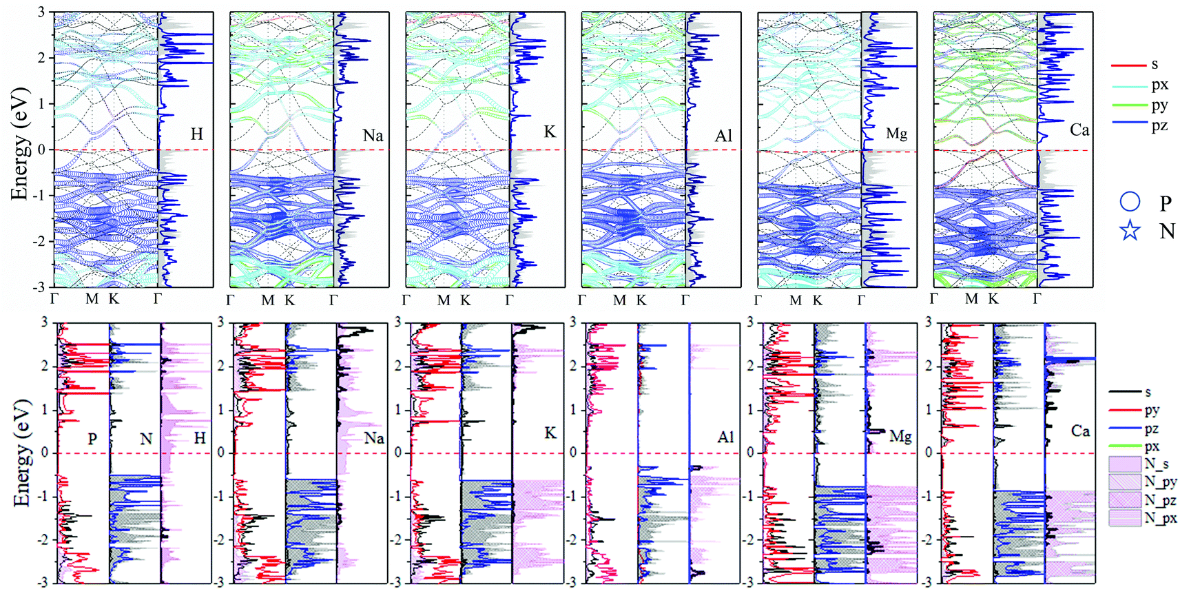 | ||
| Fig. 6 Orbital resolved band structure, DOS and PDOS of adsorbed H, Na, Mg, Al, K and Ca adatoms at the TN site. The Ef is set to zero as shown by the red dashed–dotted line. | ||
Similarly, we study the non-metal adsorption of O, F, S and Cl adatoms on TP site. 1.50–2.07 Å of dTC implies that the bonding of adatoms and neighboring P atom is chemical bonding. Meanwhile, relative value of ICOHP (Table 2) also confirms the strong interaction between adatoms and N2P6, which proves that the bond of Ad–P should be covalent bonding. As can be seen in Fig. 7, the interaction O_pz and N_pz shows the bonding component below Fermi level. This indicates that the adsorbed O atom makes the structure more stable for the O–N2P6 system. In addition, the O (S, F, and Cl)-N2P6 structures transform to p-type semiconductors after adsorbing adatoms.
 | ||
| Fig. 7 –COHP analysis of non-metal atom (H, O, P, Si) adsorbed on N2P6. | ||
Fig. 8 shows the fatband structure, DOS and PDOS of O, F, S and Cl decorated adsorbed systems. The O (S) adatom interact with neighboring P atom of N2P6via sp3-hybridization, resulting in no in-plane distortion of the structure, which is consistent with conclusion of structural change. The interaction between O/S and N2P6 are mainly comprised of the hybridization of O/S_p with P_p orbitals of the nearest atoms. Interestingly, the energy overlap ranges from −2 eV to −3 eV and −0.5 e V to 1.5 eV for the corresponding O and S adsorption system, respectively. There is no influence on electronic states near Ef because the coupling is far away from VBM/CBM. Thereby the O (S)–N2P6 system is a direct semiconductor with a bandgap of 0.259 (0.3) eV, where the VBM/CBM is located at the Γ point. On the contrary, the interaction of F/Cl with substrate eliminates the semiconducting band gap of N2P6, and achieves metallic properties. The reason can be attributed to the much higher electronegativity of F/Cl atoms.
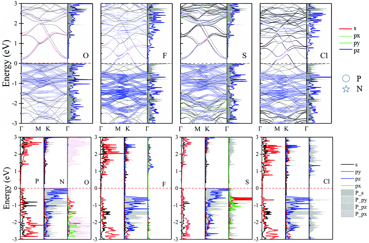 | ||
| Fig. 8 Orbital resolved band structure, DOS and PDOS of adsorbed O, F, S and Cl adatoms at the TP site. The Ef is set to zero shown by the red dashed–dotted line. | ||
Si, Ni and Cu adatoms have similar electronegativity. As shown in Fig. 9, the DOS distribution displayed in Fig. 9 focuses on understanding the electronic properties of adsorption. The band structure and DOS shift down relatively compared to pristine N2P6, and the electronic properties are totally different for Si, Ni and Cu adsorption. For example, it is quite different from the DOS before and after Si adsorption, the band structure moves down 0.5 eV after Si adsorption with respect to pristine N2P6, and reforms an indirect band gap of 0.3 eV. This proves that there is strong interaction between Si and the substrate, which reflects that the system becomes more stable after Si exposure. The corresponding ICOHP values (Table 2) and –COHP (Fig. 7) also imply the same conclusion. Moreover, the PDOS reveals that the valence electronic orbital of adatom show sp3 behavior, forming a tripod-like structure with the nearest three P atoms, and the partial hybridization of s and pxy is obvious for P atoms in N2P6. As a result, not only does the length of Si and P bond increase from 2.22 to 2.41, but also the CBM stems from the hybridization of N_s (black line, Fig. 9) with P_pz orbitals (grey grid, Fig. 9), and the VBM originates from the hybridization of P_sp and N_s, pxy orbitals. More importantly, the partial hybridization behavior of P atoms may lead to reopening of a band gap in the adsorption structure as bonding and antibonding.
 | ||
| Fig. 9 Orbital resolved band structure, DOS and PDOS of adsorbed Si, Ni and Cu adatoms at the HPP site. The zero of energy is set to Ef, shown by the red dashed–dotted line. | ||
Unlike the original N2P6, the embedding of magnetic Ni atom gives rise to some localized states, destroys the spin degeneracy of the system, and modifies the electronic and magnetic properties. The Fermi energy shift proves that Ni atoms serve as an electron donor, agrees well with charge transfer results. Energy bands split into spin up and spin down channels. The spin down (orange dotted line) channel appears the localized states which also become metallic character, while spin up (black solid line) exhibits a metal, inducing a ferromagnetic metallic with 0.59 μB magnetic moment. The DOS is shown in Fig. 9, it can be seen spin-splitting appears below Ef, with the d electronic states of Ni mainly existing below the Ef.
The Cu–N2P6 exhibits a metal character. The semiconductor to metal transition caused by charge transfer of adatoms, and adatom serves as the electron donor and transfers 0.3 electrons to the substrate, which makes Ef move up 0.5 eV (Fig. 9). Though 3d orbital states of the Cu atom has high energy values, the calculated PDOS shows 3d-orbital of Cu adatom located below −1.5 eV, which could hardly modify electron states of N2P6 around Ef.
For the P–N2P6, P adatom located on the BPP site, 2.185 Å of dTC is in conformity with the principle of P–P bond length, indicating a system of chemisorption. As shown in Fig. 7, the –COHP of P adatom and its nearest atom is similar to those of metal adatoms, but there is covalent bonding between them based on the data of ICOHP. The P–N2P6 system exhibits metal nature form the band structure, with P adatom transform 0.299e to its two nearest P atoms on N2P6 (Fig. S5, ESI†). P adatoms interact through sp3-hybridization and form two σ bonds to two neighboring P atoms (Fig. S5, ESI†).
The Li, Zn adatoms as well as the previous TN–N2P6, serve as electron donors transferring 0.883e and 0.544e to pristine N2P6, respectively. From top and side views of the structure of Li, Zn–N2P6 as shown in Fig. 10(b), we found Li adsorption of non-special site relatively increases the degree of out-plane distortion while the bucking of in-plane is very small. Zn adsorption causes distortion both in out-plane and in-plane of the structure, which results in the breaking of the system.
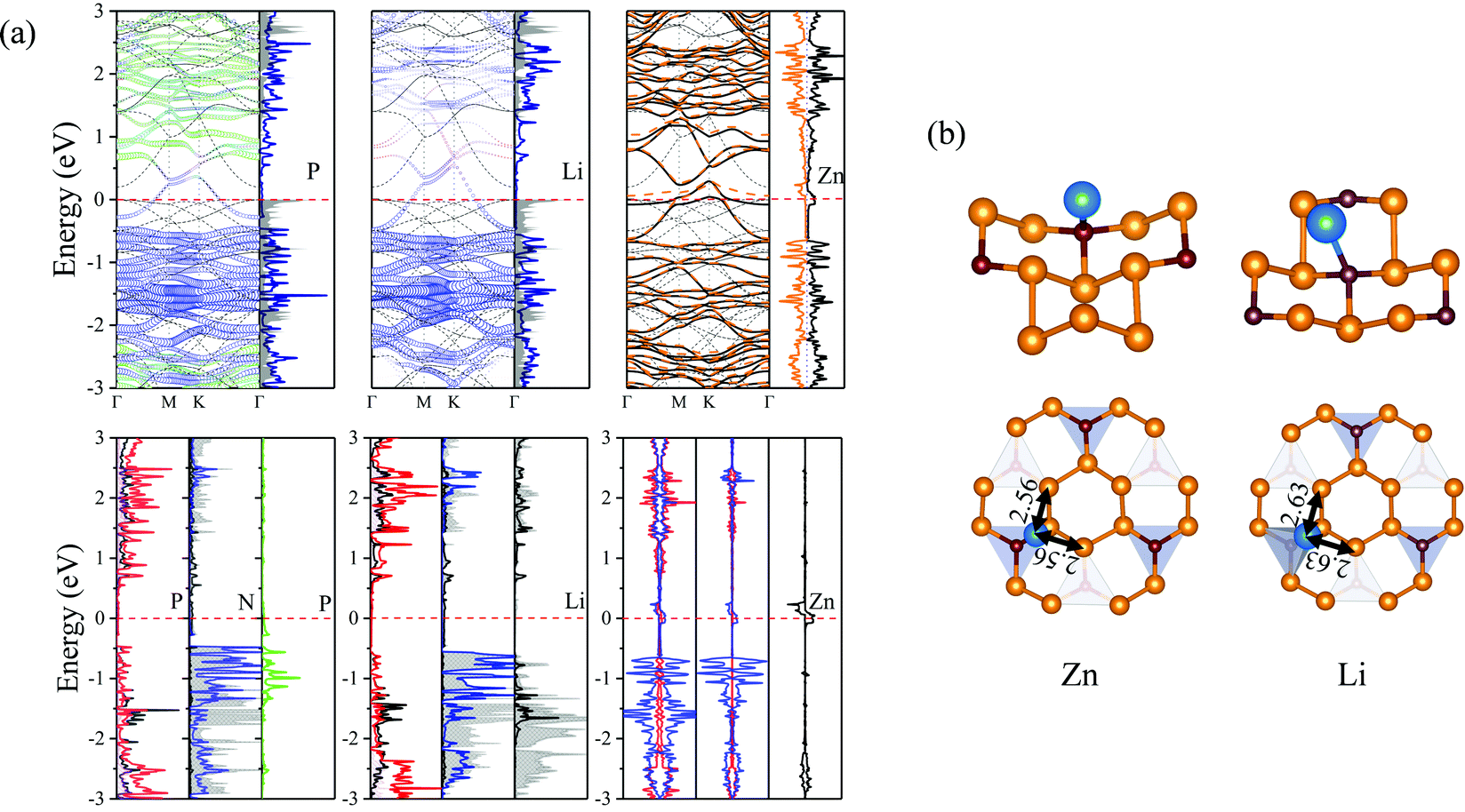 | ||
| Fig. 10 (a) Orbital resolved band structure, DOS and PDOS of their system with substrate adsorbed P, Li and Zn adatoms, respectively. The zero of energy is set to Ef, shown by the red dashed–dotted line. (b) Schematic view of the most stable site and relative position parameters of adatoms for adsorption of Zn and Li on N2P6. | ||
As shown in (Fig. 10), it can be seen the Fermi energy shifts toward low energy adsorbed Li atom from the band structure and DOS, which is similar to Na–N2P6. However, different from Ni adsorption, the ground state of Zn adsorbed by N2P6 destroys the spin degeneracy of the system which is nonmagnetic. Spin-splitting can be found in the vicinity of Ef of the main 4s-orbital peaks for Zn adatom. On the other hand, we found impurity level is introduced at the Ef level making Zn–N2P6 metal ferromagnetic. From the PDOS in Fig. 10(a), there are some localized states located at Fermi level for N and P atoms of N2P6. Metallic states originate from the Zn_4s spin up with N and P_sp spin up orbital states. The DOS of Zn adatom located below Ef illustrates the adsorption system is stable. As seen from –COHP in Fig. 5, bonding between Zn_s and N_pz is the key factor which induces spin-splitting of the band structure.
4. Conclusions
In summary, based on first-principles calculations, we have explored the effects of adsorbed atom impurities on the structural, electronic and magnetic properties of N2P6 monolayers. It is found that the pristine N2P6 is not a plane hexagonal honeycomb structure due to N/P_sp3 hybridization, and it is a semiconductor with an indirect narrow band gap of 0.21 eV. We have further systematically investigated the effect of adsorption for metal atoms (Li, Na, Mg, Al, K, Ca, Fe, Co, Ni, and Cu) and non-metal atoms (H, B, Be, O, F, S, Cl, N, P, C, and Si). The adsorption systems show different electronic and magnetic properties depending on the adatoms. The structures of N2P6 monolayers were found to remain intact, despite local deformations induced by the adsorbed atoms. In contrast, adsorption of B, Be, N, C and some transition metal adatoms (Fe, Co) will cause considerable local deformations, involving bond breaking or reorganization of N2P6 monolayers. In particular, we found that the degree of local distortion adsorption structure is related to the electronegativity of adatoms. For electronic and magnetic properties, there are considerable modifications after adsorption of adatoms. The band gap of N2P6 can be modified and the system will transform to metal, magnetic metal, half-metal or remain a semiconductor depending on the species of adatoms. Moreover, through calculating the PDOS and –COHP, we verify the stability of the adsorption systems, and also reveal the adsorption mechanism. Our research provides a detailed understanding of the electronic structure of N2P6 and how it is modified by adsorption of various atoms, which should be very useful for studies of semiconductor photocatalytic materials and gas sensors in the future.Conflicts of interest
There are no conflicts to declare.Acknowledgements
This work is supported by the Program of Shanghai Normal University (309-AC7001-21-003041).References
- K. S. Novoselov, A. K. Geim, S. V. Morozov, D. Jiang, Y. Zhang and S. V. Dubonos, Electric Field Effect in Atomically Thin Carbon Films, Science, 2004, 306(5696), 666–669 CrossRef CAS PubMed.
- X. Li and H. Zhu, Two-dimensional MoS2: Properties, preparation, and applications, J. Materiomics, 2015, 1(1), 33–44 CrossRef.
- M. S. Xu, T. Liang, M. M. Shi and H. Z. Chen, Graphene-Like Two-Dimensional Materials, Chem. Rev., 2013, 113(5), 3766–3798 CrossRef CAS PubMed.
- K. Hantanasirisakul and Y. Gogotsi, Electronic and Optical Properties of 2D Transition Metal Carbides and Nitrides (MXenes), Adv. Mater., 2018, 30(52), e1804779 CrossRef PubMed.
- M. Faraji, A. Bafekry, M. M. Fadlallah, F. Molaei, N. N. Hieu, P. Qian, M. Ghergherehchi and D. Gogova, Surface modification of titanium carbide MXene monolayers (Ti2C and Ti3C2) via chalcogenide and halogenide atoms, Phys. Chem. Chem. Phys., 2021, 23(28), 15319–15328 RSC.
- X. Huang, Z. Y. Yin, S. X. Wu, X. Y. Qi, Q. Y. He, Q. C. Zhang, Q. Y. Yan, F. Boey and H. Zhang, Graphene-Based Materials: Synthesis, Characterization, Properties, and Applications, Small, 2011, 7(14), 1876–1902 CrossRef CAS PubMed.
- Q. H. Wang, K. Kalantar-Zadeh, A. Kis, J. N. Coleman and M. S. Strano, Electronics and optoelectronics of two-dimensional transition metal dichalcogenides, Nat. Nanotechnol., 2012, 7(11), 699–712 CrossRef CAS PubMed.
- K. Zollner, P. E. F. Junior and J. Fabian, Strain-tunable orbital, spin-orbit, and optical properties of monolayer transition-metal dichalcogenides, Phys. Rev. B, 2019, 100(19), 195126 CrossRef CAS.
- G. R. Bhimanapati, Z. Lin and V. Meunier, Recent advances in two-Dimensional materials beyond graphene, ACS Nano, 2015, 9(12), 11509–11539 CrossRef CAS PubMed.
- X. G. Li, W. T. Bi, L. Zhang, S. Tao, W. S. Chu, Q. Zhang, Y. Luo, C. Z. Wu and Y. Xie, Single-Atom Pt as Co-Catalyst for Enhanced Photocatalytic H-2 Evolution, Adv. Mater., 2016, 28(12), 2427–2431 CrossRef CAS PubMed.
- L. J. Li, E. C. T. O’Farrell, K. P. Loh, G. Eda, B. Ozyilmaz and A. H. C. Neto, Controlling many-body states by the electric-field effect in a two-dimensional material, Nature, 2016, 529(7585), 185–189 CrossRef CAS PubMed.
- H. W. Guo, Z. Hu, Z. B. Liu and J. G. Tian, Stacking of 2D Materials, Adv. Funct. Mater., 2020, 31(4), 2007810 CrossRef.
- X. F. Yu, Y. C. Li, J. B. Cheng, Z. B. Liu, Q. Z. Li, W. Z. Li, X. Yang and B. Xiao, Monolayer Ti(2)CO(2): A Promising Candidate for NH(3) Sensor or Capturer with High Sensitivity and Selectivity, ACS Appl. Mater. Interfaces, 2015, 7(24), 13707–13713 CrossRef CAS PubMed.
- Y. Zhang, W. Zeng and Y. Li, NO2 and H2 sensing properties for urchin-like hexagonal WO3 based on experimental and first-principle investigations, Ceram. Int., 2019, 45(5), 6043–6050 CrossRef CAS.
- F. Bonaccorso, Z. Sun, T. Hasan and A. C. Ferrari, Graphene photonics and optoelectronics, Nat. Photonics, 2010, 4(9), 611–622 CrossRef CAS.
- X. Wang, L. J. Zhi and K. Mullen, Transparent, conductive graphene electrodes for dye-sensitized solar cells, Nano Lett., 2008, 8(1), 323–327 CrossRef CAS PubMed.
- F. Bonaccorso, L. Colombo, G. H. Yu, M. Stoller, V. Tozzini, A. C. Ferrari, R. S. Ruoff and V. Pellegrini, Graphene, related two-dimensional crystals, and hybrid systems for energy conversion and storage, Science, 2015, 347, 6217 CrossRef PubMed.
- R. Kolahchi, B. Keshtegar and M. H. Fakhar, Optimization of dynamic buckling for sandwich nanocomposite plates with sensor and actuator layer based on sinusoidal-visco-piezoelasticity theories using Grey Wolf algorithm, J. Sandwich Struct. Mater., 2020, 22(1), 3–27 CrossRef.
- J. T. Robinson, F. K. Perkins, E. S. Snow, Z. Q. Wei and P. E. Sheehan, Reduced Graphene Oxide Molecular Sensors, Nano Lett., 2008, 8(10), 3137–3140 CrossRef CAS PubMed.
- M. Y. Han, B. Ozyilmaz, Y. B. Zhang and P. Kim, Energy band-gap engineering of graphene nanoribbons, Phys. Rev. Lett., 2007, 98, 20 Search PubMed.
- X. D. Zhang and Y. Xie, Recent advances in free-standing two-dimensional crystals with atomic thickness: design, assembly and transfer strategies, Chem. Soc. Rev., 2013, 42(21), 8187–8199 RSC.
- A. Bafekry, M. Ghergherehchi, S. F. Shayesteh and F. M. Peeters, Adsorption of molecules on C3N nanosheet: a first-principles calculations, Chem. Phys., 2019, 526 Search PubMed.
- A. Bafekry, C. Stampfl, B. Akgenc and M. Ghergherehchi, Control of C3N4 and C4N3 carbon nitride nanosheets' electronic and magnetic properties through embedded atoms, Phys. Chem. Chem. Phys., 2020, 22(4), 2249–2261 RSC.
- A. Bafekry, C. Stampfl, M. Ghergherehchi and S. F. Shayesteh, A first-principles study of the effects of atom impurities, defects, strain, electric field and layer thickness on the electronic and magnetic properties of the C2N nanosheet, Carbon, 2020, 157, 371–384 CrossRef CAS.
- Y. Gui, X. Peng, K. Liu and Z. Ding, Adsorption of C2H2, CH4 and CO on Mn-doped graphene: atomic, electronic, and gas-sensing properties, Phys. E, 2020, 119 Search PubMed.
- S. Manzeli, D. Ovchinnikov, D. Pasquier, O. V. Yazyev and A. Kis, 2D transition metal dichalcogenides, Nat. Rev. Mater., 2017, 2(8), 17033 CrossRef CAS.
- A. Castellanos-Gomez, Black Phosphorus: Narrow Gap, Wide Applications (vol 6, pg 4280, 2015), J. Phys. Chem. Lett., 2015, 6(23), 4873 CrossRef CAS PubMed.
- J. Zhu, G. Xiao and X. Zuo, Two-Dimensional Black Phosphorus: An Emerging Anode Material for Lithium-Ion Batteries, Nanomicro Lett., 2020, 12(1), 120 CAS.
- Y. Zhang, Q. Jiang, P. Lang, N. Yuan and J. Tang, Fabrication and applications of 2D black phosphorus in catalyst, sensing and electrochemical energy storage, J. Alloys Compd., 2021, 850 Search PubMed.
- S. X. Yang, C. B. Jiang and S. H. Wei, Gas sensing in 2D materials, Appl. Phys. Rev., 2017, 4(2), 1–34 Search PubMed.
- Y. Q. Cai, Q. Q. Ke, G. Zhang and Y. W. Zhang, Energetics, Charge Transfer, and Magnetism of Small Molecules Physisorbed on Phosphorene, J. Phys. Chem. C, 2015, 119(6), 3102–3110 CrossRef CAS.
- L. Z. Kou, T. Frauenheim and C. F. Chen, Phosphorene as a Superior Gas Sensor: Selective Adsorption and Distinct I–V Response, J. Phys. Chem. Lett., 2014, 5(15), 2675–2681 CrossRef CAS PubMed.
- A. N. Abbas, B. L. Liu, L. Chen, Y. Q. Ma, S. Cong, N. Aroonyadet, M. Kopf, T. Nilges and C. W. Zhou, Black Phosphorus Gas Sensors, ACS Nano, 2015, 9(5), 5618–5624 CrossRef CAS PubMed.
- A. Singh, H. Bae, S. Lee, K. Shabbiri, T. Hussain and H. Lee, Highly sensitive and selective sensing properties of modified green phosphorene monolayers towards SF6 decomposition gases, Appl. Surf. Sci., 2020, 512 Search PubMed.
- A. J. Yang, D. W. Wang, X. H. Wang, D. Z. Zhang, N. Koratkar and M. Z. Rong, Recent advances in phosphorene as a sensing material, Nano Today, 2018, 20, 13–32 CrossRef CAS.
- N. Tan, C. Y. He, C. Tang and J. X. Zhong, First-principles study of the structures and fundamental electronic properties of two-dimensional P0.5As0.5 alloy, Phys. Status Solidi B, 2017, 254(10), 1700157 CrossRef.
- Y. Dong, X. Lv, L. Yu, F. Li and J. Gong, Two-dimensional phosphorus-based binary nanosheets for photocatalyzing water splitting: a first-principles study, Chem. Phys. Lett., 2021, 772 Search PubMed.
- D. Laniel, B. Winkler, T. Fedotenko, A. Pakhomova, S. Chariton, V. Milman, V. Prakapenka, L. Dubrovinsky and N. Dubrovinskaia, High-Pressure Polymeric Nitrogen Allotrope with the Black Phosphorus Structure, Phys. Rev. Lett., 2020, 124(21), 216001 CrossRef CAS PubMed.
- K. Landskron, H. Huppertz, J. Senker and W. Schnick, High-Pressure Synthesis of gamma-P3 N5 at 11 GPa and 1500 degrees C in a Multianvil Assembly: A Binary Phosphorus(V) Nitride with a Three-Dimensional Network Structure from PN4 Tetrahedra and Tetragonal PN5 Pyramids, Angew. Chem., Int. Ed., 2001, 40(14), 2643–2645 CrossRef CAS PubMed.
- M. Naseri, A. Bafekry, M. Faraji, D. M. Hoat, M. M. Fadlallah, M. Ghergherehchi, N. Sabbaghi and D. Gogova, Two-dimensional buckled tetragonal cadmium chalcogenides including CdS, CdSe, and CdTe monolayers as photo-catalysts for water splitting, Phys. Chem. Chem. Phys., 2021, 23(21), 12226–12232 RSC.
- A. Bafekry, M. Faraji, M. M. Fadlallah, B. Mortazavi, A. A. Ziabari, A. B. Khatibani, C. V. Nguyen, M. Ghergherehchi and D. Gogova, Point Defects in a Two-Dimensional ZnSnN2 Nanosheet: A First-Principles Study on the Electronic and Magnetic Properties, J. Phys. Chem. C, 2021, 125(23), 13067–13075 CrossRef CAS.
- A. Bafekry, M. Faraji, M. M. Fadlallah, H. R. Jappor, N. N. Hieu, M. Ghergherehchi, S. A. H. Feghhi and D. Gogova, Prediction of two-dimensional bismuth-based chalcogenides Bi2X3 (X = S, Se, Te) monolayers with orthorhombic structure: a first-principles study, J. Phys. D: Appl. Phys., 2021, 54(39), 395103 CrossRef CAS.
- A. Bafekry, I. A. Sarsari, M. Faraji, M. M. Fadlallah, H. R. Jappor, S. Karbasizadeh, V. Nguyen and M. Ghergherehchi, Electronic and magnetic properties of two-dimensional of FeX (X = S, Se, Te) monolayers crystallize in the orthorhombic structures, Appl. Phys. Lett., 2021, 118(14), 143102 CrossRef CAS.
- K. Niwa, Y. Iijima, M. Ukita, R. Toda, K. Toyoura, T. Sasaki, K. Matsunaga, N. A. Gaida and M. Hasegawa, Nitriding synthesis and structural change of phosphorus nitrides at high pressures, J. Raman Spectrosc., 2021, 52(5), 1064–1072 CrossRef CAS.
- Y. C. Wang, M. S. Miao, J. Lv, L. Zhu, K. T. Yin, H. Y. Liu and Y. M. Ma, An effective structure prediction method for layered materials based on 2D particle swarm optimization algorithm, J. Chem. Phys., 2012, 137(22), 224108 CrossRef PubMed.
- X. Y. Luo, J. H. Yang, H. Y. Liu, X. J. Wu, Y. C. Wang, Y. M. Ma, S. H. Wei, X. G. Gong and H. J. Xiang, Predicting Two-Dimensional Boron-Carbon Compounds by the Global Optimization Method, J. Am. Chem. Soc., 2011, 133(40), 16285–16290 CrossRef CAS PubMed.
- B. Delley, An All-Electron Numerical-Method for Solving the Local Density Functional for Polyatomic-Molecules, J. Chem. Phys., 1990, 92(1), 508–517 CrossRef CAS.
- J. P. Perdew, K. Burke and M. Ernzerhof, Generalized gradient approximation made simple (vol 77, pg 3865, 1996), Phys. Rev. Lett., 1997, 78(7), 1396 CrossRef CAS.
- A. Bafekry, S. Karbasizadeh, C. Stampfl, M. Faraji, D. M. Hoat, I. A. Sarsari, S. A. H. Feghhi and M. Ghergherehchi, Two-dimensional Janus semiconductor BiTeCl and BiTeBr monolayers: a first-principles study on their tunable electronic properties via an electric field and mechanical strain, Phys. Chem. Chem. Phys., 2021, 23(28), 15216–15223 RSC.
- H. C. Chow and S. H. Vosko, Special Points for Two-Dimensional Brillouin-Zone or Wigner-Seitz Cell Integrations, Can. J. Phys., 1980, 58(4), 497–503 CrossRef CAS.
- R. S. Mulliken, Electronic Population Analysis on Lcao-Mo Molecular Wave Functions.4. Bonding and Antibonding in Lcao and Valence-Bond Theories, J. Chem. Phys., 1955, 23(12), 2343–2346 CrossRef CAS.
- S. Maintz, V. L. Deringer, A. L. Tchougreeff and R. Dronskowski, LOBSTER: A Tool to Extract Chemical Bonding from Plane-Wave Based DFT, J. Comput. Chem., 2016, 37(11), 1030–1035 CrossRef CAS PubMed.
- R. Nelson, C. Ertural, J. George, V. L. Deringer, G. Hautier and R. Dronskowski, LOBSTER: Local orbital projections, atomic charges, and chemical-bonding analysis fromprojector-augmented-wave-baseddensity-functional theory, J. Comput. Chem., 2020, 41(21), 1931–1940 CrossRef CAS PubMed.
- C. Liu, T. Hu, Y. Wu, H. Gao, Y. Yang and W. Ren, 2D selenium allotropes from first principles and swarm intelligence, J. Phys.: Condens. Matter, 2019, 31(23), 235702 CrossRef CAS PubMed.
- K. Pu, X. Dai, D. Jia, W. Tao, F. Liu, X. Zhang, J. Song, T. Zhao and Y. Hao, Structural, electrical and optical properties of halogen doped phosphorene based on density functional theory, J. Alloys Compd., 2020, 812 Search PubMed.
- S. Steinberg and R. Dronskowski, The Crystal Orbital Hamilton Population (COHP) Method as a Tool to Visualize and Analyze Chemical Bonding in Intermetallic Compounds, Crystals, 2018, 8(5), 225 CrossRef.
Footnote |
| † Electronic supplementary information (ESI) available. See DOI: 10.1039/d1cp03211a |
| This journal is © the Owner Societies 2021 |