
 Open Access Article
 This Open Access Article is licensed under a Creative Commons Attribution-Non Commercial 3.0 Unported Licence
First principles simulations of microscopic mechanisms responsible for the drastic reduction of electrical deactivation defects in Se hyperdoped silicon
Alberto
Debernardi

CNR-IMM, Unit of Agrate Brianza, via C. Olivetti 2, 20864 Agrate Brianza (MB), Italy. E-mail: alberto.debernardi@mdm.imm.cnr.it
First published on 8th October 2021
Abstract
By first principles simulations we systematically investigate Se hyperdoped silicon by computing, for different types of Se complexes, the formation energy as a function of dopant concentration. We identify the microscopic mechanisms responsible for the dramatic reduction of electrical deactivation defects as the dopant concentration approaches the critical value, xc, at which the insulator-to-metal transition occurs. We discuss the electrical properties of Se point defects and Se complexes, shedding light on the formation and the nature of the impurity band in the bandgap and how the presence of different types of complexes may increase the broadening of the impurity band and affects the insulator-to-metal transition. We identify the best doping range in which the properties of the impurity band can be engineered according to the needs of the electronic industry. Simulations of the structural properties of the complexes complete the work. Our findings are relevant for intermediate impurity band applications.
I Introduction
Silicon hyperdoped (i.e., doped beyond the solid solubility limit) with donor impurities is attracting increasing attention from the electronic industry and materials science community because it is a promising candidate as a building block for the conception of new electronic devices ranging from infrared absorbers,1–3 to intermediate band photovoltaics4,5 to ultra-scaled nano-electronics6. The latter application is motivated by the continuous scaling down of Si-based transistors in on-chip complementary metal oxide semiconductor (CMOS) devices, which are approaching the 2 nm technology node. Therefore, the next generation of ultra-scaled CMOS devices requires extremely high free-electron densities, of the order of 1021 cm−3 (i.e. one electron per nm3) to ensure sufficient free carriers in a transistor to work.7,8Shallow donors, such as group V elements (P, As, or Sb), are traditionally employed as dopants in Si for their low ionization energy, low diffusivity and suitable solid solubility. Unfortunately, their free-electron concentration saturates at around 5 × 1020 cm−3:9,10 beyond this concentration the introduction of further donors does not generate free carriers, thus providing an upper limit for the electron density, preventing the realization of nanometer-size devices.
In the last few decades, experimental11–13 and theoretical14–16 works studied the microscopic mechanisms responsible for saturation of free-electron concentration in group V dopants in Si. The saturation has been attributed to the formation of electrical deactivation defects. According to the literature, these defects have been identified with different types of substitution complexes: the Asn–VSi (n ≤ 4) model (the clustering around a Si vacancy, VSi, surrounded by As atoms,12,14–23 also invoked to interpret Sbn–VSi clusters24); the dimers (substitutional dopant in nearest neighbor (NN) lattice sites)25 and the defects containing pairs of separated dopant atoms (in next NN lattice sites) without vacancies.25,26 These group V complexes introduce deep acceptor states in the bandgap that deactivate free carriers, thus preventing high electron concentrations.25,26
At variance, chalcogen impurities (group VI elements: S, Se, and Te) are deep donors in Si, having ionization energy of a few hundreds of meV at low concentration, while at high concentration they can induce free electrons (in excess of 1020 cm−3) in Si, accompanied by an insulator-to-metal transition (IMT).27,28 Chalcogens show superior electronic properties as Si hyper-dopants than traditional group V elements: a Te concentration of 1.25 × 1021 cm−3 has been reached in hyperdoped Si without showing any sign of saturation,6,29 while the electron concentration (8.1 × 1020 cm−3![[thin space (1/6-em)]](https://www.rsc.org/images/entities/char_2009.gif) 6) in the same samples nearly scored the target of 1021 cm−3 required for the next generation of the Si technology node.7,9,30
6) in the same samples nearly scored the target of 1021 cm−3 required for the next generation of the Si technology node.7,9,30
Furthermore, hyper-doping establishes a new materials playground to investigate impurity mediated IMTs in semiconductors, that has been largely studied both for its interest in fundamental physics and for its relevance in technological applications. Previous studies about IMT in S27,31 and Se28 hyperdoped Si have been focused on the single substitutional impurities, while recently, first principles simulations have enlightened the role of dimers as a driving force of IMT in Te hyperdoped Si.6,29
Computational studies are therefore desirable to validate this scenario, by considering other chalcogen dopants, and additional types of chalcogen complexes, to provide novel insights into the microscopic mechanisms governing the hyperdoped regime in Si.
In this work we present first principles simulations of the formation energy of different complexes in Se hyperdoped Si in a wide range of dopant concentrations.
This article is structured as follows: in Section II we describe the computational techniques used in the work; in Section III.A we display our results for the formation energy of the different types of defects investigated as a function of dopant concentration; for each defect, we present our first principles results for the electronic, and the structural properties, respectively in Sections III.B and III.C. In Section IV we discuss our finding in relation to applications in which Se hyperdoped silicon can be used as building block in innovative devices based on the formation of an intermediate impurity band in the electronic gap. Finally, in Section V we present our conclusions and summarize our results.
II Computational methods
In our simulations we consider Se interstitial ISe, single Se substitutional, SeSi, Se dimers SeSi–SeSi and complexes formed by a Si vacancy VSi surrounded by m Se atoms, denoted as (SeSi)m–VSi, m = 1, 2, 3, 4. Although the latter complexes have been extensively studied for group V donors (mainly As), the possible role of the clustering of chalcogen atoms around a vacancy seems still unexplored by ab initio simulations. Geometrical models of neutral single vacancy-selenium complexes are determined from first principles by plane-wave pseudopotentials techniques. We will present the formation energy of these complexes as a function of the Se concentration, and we will discuss electrical properties to enlighten the advantages of chalcogen atoms as dopants in forthcoming nanometer-size devices based on hyperdoped Si.Our simulations are obtained using the super-cell method within the single complex model (SCM); accuracy and limit of SCM, and all computational details are discussed in Appendix A.
III Results
A Defect formation energy
We denote with D a generic defect among the ones considered in the present work (i.e. D ∈ ISe, SeSi, SeSi–SeSi and (SeSi)m–VSi, m = 1, 2, 3, and 4). For the defect D, the formation energy per Se atom as a function of Se concentration x, in hyperdoped silicon (Si1−xSex), reads| ΔEFormD(x) ≡ [ED(x) − NSiμSi − NSeμSe]/NSe | (1) |
In Fig. 1 and 2 we display our computed formation energy at different doping concentrations for all complexes investigated. Note that, accordingly to the choice of the chemical potentials, the zero of the energy corresponds to the phase separation of Si1−xSex into bulk Si and SiSe2, and all Se complexes present positive formation energy, in agreement with the experimental fact that, in the concentration range considered, Si is doped beyond the Se solid solubility limit.6,32
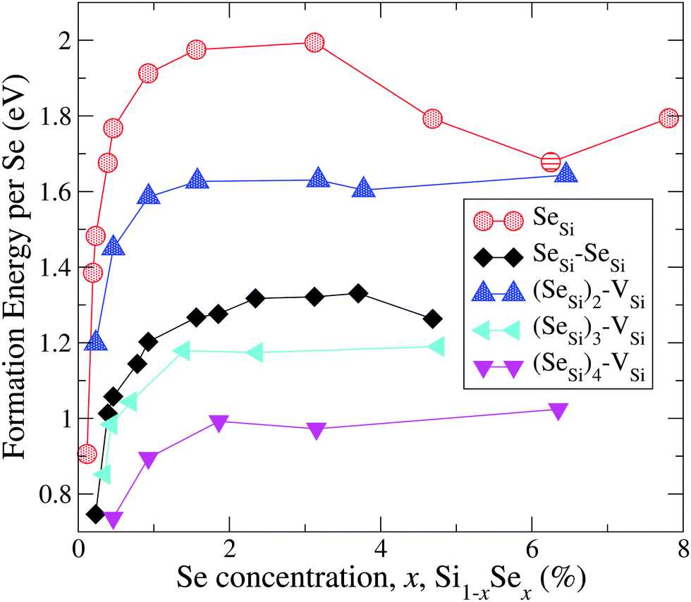 | ||
| Fig. 1 Formation energy (per atom) of Se substitutional impurities and their complexes with a silicon vacancy. Solid lines are a guide for the eye. | ||
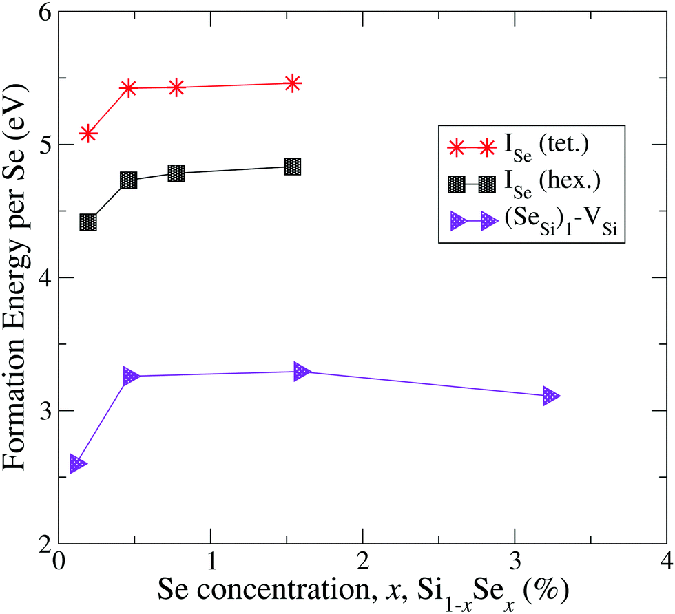 | ||
| Fig. 2 Formation energy (per atom) of Se interstitials and the complex formed by Se substitutional with a silicon vacancy. | ||
By the comparison of the energy scales of the two figures we can immediately appreciate that at high concentration (x ≳ 0.45 at%) the formation energies of the complexes displayed in Fig. 2 (ISe and SeSi–VSi) are more than one eV higher that the ones of Fig. 1, thus making unlikely, at least at high concentration, the formation of the complexes displayed in Fig. 2, as discussed below.
For convenience, in the following discussion, we distinguish, for each type of defect D, three different ranges of doping: (1) the highly diluted range (x ≪ 1), in which the average distance between different complexes is so high that the complexes can be considered as non-interacting; (2) the interaction range, in which the average distances between randomly distributed complexes allow a non-negligible overlap of the wave-function of different complexes, producing a impurity band (IB) in the gap; and (3) the fully metallic range for concentration greater than the concentration xM(D) at which the IB merges into the conduction band; in this range the electrons originating from the IB are de-localized in the conduction bands thus contributing to the metallic behaviors.
The ab initio simulation of a highly diluted range, requiring enormous size super-cells, is beyond the scope of the present work, which is focused on the interaction and the metallic ranges corresponding to hyper-doping. Donor complexes in highly diluted range have localized wave-functions, producing energy levels in the bandgap having sharp (zero or negligible) linewidth due to negligible overlap between the wave-functions of different defects. In this range the formation energy is almost equal to the one of the isolated defect, ΔEFormD(0).
As the concentration increases (interaction range), the interaction between neighboring complexes produces an IB whose width increases for increasing overlap, and the formation energy steeply increases up to the concentration at which the system presents metallic states delocalized in the whole crystal.
In the fully metallic range, for x > xM, the IB is merged into the conduction band providing conduction electrons and eventually contributing to a metallic screening of the impurity complex, and ΔEFormD(x) is a smooth function of x.
As it will be illustrated in the next section, the different types of complexes, can be divided in two sets: complexes that in the interaction range have an insulating IB, denoted as Dins and complexes that in the interaction range have a metallic IB, denoted as Dmet. For the latter complexes, we define xs(Dmet) as the concentration at which ΔEFormD(x) becomes smooth; in general, xs(Dmet) ≲ xM(Dmet), the non-equality holds probably as a consequence of the screening effects due to the formation of a metallic band.
In general, for all type of complexes investigated, the formation energy increases monotonically with increasing concentration; ΔEFormD(x) is steep in the interaction range (up to xs for Dmet), while it is rather flat in the metallic range. The decrease of ΔEFormSeSi(x) for x > 3 at% is probably due to the mutual interaction of different SeSi, that above the xM(SeSi) produces a lowering of the formation energy approaching the one of dimers as the concentration increases.
These differences in ΔEFormD(x) explain the prevalence of complexes involving substitutional Se with respect to Se interstitials in the metallic range, detected in experimental studies, since according to our simulations the former complexes have lower formation energy in the region where ΔEFormD(x) is flat. Although similar differences in ΔEFormD(x) can be also noticed in the lower values of x range considered, a local fluctuation of the concentration Δx, provided by the random distribution of dopants, can cause a significant variation in the formation energy of the complex if x is within the interaction range in which ΔEFormD(x) is steep, thus preventing the complexes having the lowest ΔEFormD(x) to become the dominant ones.
To better illustrate this concept, we consider two complexes D1 and D2 for which 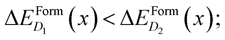 if x is within the steep range of ΔEFormD(x) and a local increase (decrease) Δx1 (−Δx2) occurs in a region of the crystal where the complexes D1 (D2) are present, this fluctuation can produce
 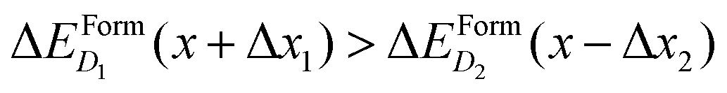 .
.
At variance, if x is within the metallic range, where ΔEFormD(x) is smooth, the formation energy is only slightly affected by a local fluctuation of x (in fact, in the smooth range a local fluctuation does not change the inequality  ), and thus the complexes having lowest ΔEFormD(x) are the predominant ones that we expect to detect in an experiment.
The complexes formed by one substitutional Se nearest-neighbour (NN) to a Si vacancy, SeSi–VSi, and the Se interstitial, ISe, in the hexagonal or in the tetrahedral position, have significantly higher formation energy than the other complexes investigated; for x ≳ 0.45 at% the formation energy of these complexes is smooth, and consequently, the formation of these complexes is unlikely, explaining the dramatic reduction of interstitial Se at these concentrations as experimentally detected in Se hyperdoped Si.32,33 A similar mechanism has been also found in Te hyperdoped Si6 (by comparing ΔEFormD of ITe, TeSi, TeSi–TeSi).
B Electronic bandstructure
To analyze the electronic properties of different defects, in Fig. 3 and 4 we display the Density of States (DOS) of the different types of complexes studied for x ∈ [0.44–0.46] at%. With this choice of x, all types of defects considered have equal or very similar Se concentration thus allowing the comparison between the IB of different complexes.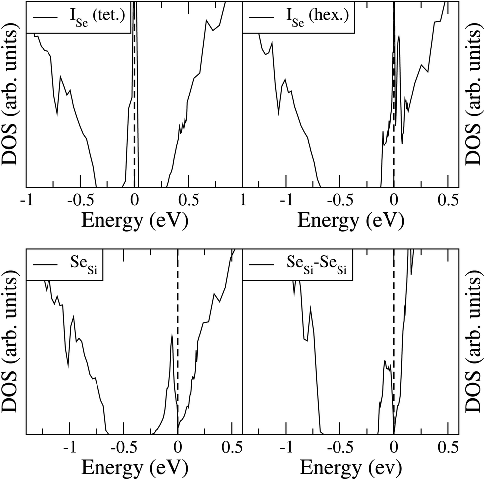 | ||
| Fig. 3 Electronic DOS of Si1−xSex for Se interstitial in the tetrahedral and hexagonal positions at x = 0.461 at%, and for substitutional single SeSi and SeSi–SeSi dimers at x = 0.463 at%. | ||
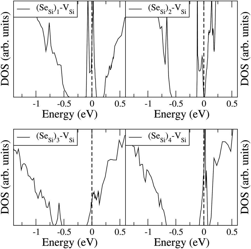 | ||
| Fig. 4 Electronic DOS of Si1−xSex for (SeSi)m–VSi, with m = 1, 2, 3, and 4 at x ≃ 0.465; 0.464; 0.438; and 0.463 at%, respectively. | ||
At this concentration, the IB of ISe in the hexagonal position and the IB of (SeSi)3–VSi have already been merged with the conduction band, while the IBs formed by the other complexes are within the bandgap originated from the Si gap. (SeSi)4–VSi has a shallow metallic IB. At variance, ISe in the tetrahedral position and (SeSi)1–VSi have metallic IB deep in the bandgap, and both complexes are double acceptors, thus acting as deactivation centers for electronic carriers. According to Fig. 2 the formation energy of the latter two complexes for x ≳ 0.45 at% is flat, in agreement with the fact that the complexes present metallic behaviors, and thus produces a drastic reduction of undesired deactivation centers for x > 0.45 at%.
Fig. 3 and 4 show that SeSi, SeSi–SeSi, and (SeSi)2–VSi form insulating IBs, occupied with two electrons per complex.
While the IB filling with two electrons per SeSi is simply understood since Se has two more valence electrons than Si thus acting as double donor, the IB filling with two electrons per SeSi–SeSi, can be explained as follows: three electrons from each of the two NN SeSi are involved in the bond with the three NN of the host Si, while two electrons of each SeSi are involved in the Se–Se double bond in a similar way to that in Se2 molecule34. In fact, according to our simulations the value of the Se–Se bond of Se2 molecule is 2.18 Å, quite close (∼10% smaller) to the value of the Si-Si bond in bulk Si, which is 2.37 Å. This bond filling leaves one unpaired electron for each SeSi, thus accounting for the fact that SeSi–SeSi is a double donor in Si (i.e. each Se provide one electron to the conduction band). Probably, a similar mechanism can also be invoked for (SeSi)2–VSi. Consequently, the latter two complexes, each involving two substitutional Se, donate one electron per – Se atom to the conduction band.
The Fermi energy intersects the IB of ISe in tetrahedral position and the IB of (SeSi)1–VSi; each IB is deep in the bandgap and both complexes are double acceptors, thus acting as deactivation centers for electronic carriers. Notice that for (SeSi)1–VSi the Fermi energy separates two well resolved peaks in the DOS at the IB, a reminiscence of the separated filled and empty electronic levels of isolated complex, now merged in a metallic IB. As shown in Fig. 2, for these complexes, the concentration x ≃ 0.45 at% corresponds to the flat range of the formation energy, in agreement with the fact that the complexes present metallic behaviors, as discussed above.
Similar results can be deduced from the analysis of the electronic bandstructure. The interested reader can find a detailed discussion of the electronic bands in relation to the electrical properties of the different types of defects in Appendix C.
C Geometry of Complexes involving substitutional Se
In Tables 1 and 2, for x ≃ 0.45 at%, we display the geometry of fully relaxed complexes involving substitutional Se, reporting the distances d between all the atoms of the complex. In the first columns of the tables, we report the distances d(p.d. −X) between the point defect (p.d. = VSi,SeSi) and the NN atoms forming the complex (X = SeSi,Si, assuming the vacant atom lying at the ideal position in the pristine lattice). In the last columns we report the distances d(X–X) between the four atoms (6 distances) neighboring VSi (SeSi) or between the six Si (15 distances) NN to Se in SeSi–SeSi. Note that while the distances correspond to relaxed positions, the symbol NNnlabels the atoms according to the ideal positions in the pristine lattice in the n-th NN shell from the p.d. The (SeSi)m–VSi complexes show an inward relaxation of Se toward the vacancy. At variance, for SeSi the relaxed d(Se–Si) is 8% isotropically larger than the simulated ideal Si–Si bond (2.37 Å).| Complex | Conc. (%) | d(VSi–Se) | d(VSi–Si) | d(Se–Se) | d(Se–Si) | d(Si–Si) |
|---|---|---|---|---|---|---|
| (SeSi)1–VSi | 0.465 | 2.30 (1) | 2.09 (3) | — | 3.63 (3) | 3.37 (3) |
| (SeSi)2–VSi | 0.464 | 2.25 (2) | 2.06 (2) | 3.69 (1) | 3.52 (4) | 3.35 (1) |
| (SeSi)3–VSi | 0.438 | 2.29 (3) | 2.12 (1) | 3.74 (3) | 3.61 (3) | — |
| (SeSi)4–VSi | 0.463 | 2.33 (4) | — | 3.80 (6) | — | — |
| Near. neigh. shell | NN | NN2 | ||||
| Complex | Conc. (%) | d(Se–Se) | d(Se–Si) | d(Si–Si) | |||
|---|---|---|---|---|---|---|---|
| SeSi | 0.463 | — | 2.57 (4) | 4.19 (12) | — | — | — |
| SeSi–SeSi | 0.463 | 3.15 (1) | 2.44 (3) | 4.37 (3) | 4.12 (6) | 4.82 (6) | 6.34 (3) |
| Near. neigh. shell | NN | NN2 | NN3 | NN4 | |||
Since they can be measured by Rutherford back-scattering spectrometry in channeling geometry (RBS-C), we report, for x ≃ 0.45 at%, the atomic displacements of Se from the ideal position in the pristine lattice. While for (SeSi)m–VSi, m = 1, 3, or 4, the atomic displacement is very small (about 0.06, 0.08, and 0.04 Å for m = 1, 3, and 4, respectively) for SeSi–SeSi and (SeSi)2–VSi the Se displacement is 0.39 Å, and 0.12 Å, respectively, representing a fingerprint of the peculiar bond formed by couples of chalcogen donors in Si. Similar values of Se displacements are obtained for other concentrations.
IV Discussion
We briefly discuss our finding in view of possible applications of chalcogen hyperdoped Si as the building block in broad band infra-red detectors or intermediate band photo-voltaics. Both applications are based on the formation of a relatively shallow IB.At room temperature – the usual device working temperature – all IB electrons are thermally excited in the conduction band, while the absorption of infra-red radiation (or of sunlight to photo-generate electric current for photo-voltaics) is produced by the excitation of valence-band electrons into the IB.
Our goal is to determine the best doping range for these applications.
Assuming a uniform random distribution of substitutional Se in the lattice sites, the complexes involving three or more donors are extremely unlikely (for a quantitative analysis see Appendix B). The complexes of Fig. 1 involving up to two Se have insulating IB, for these Dins defects we found
| 0.46 at% ≅ xM(SeSi) < xM((SeSi)2–VSi) < xM(SeSi–SeSi) ≅ 0.93 at% | (2) |
According to the above analysis for x ≳ 0.46 at% the system presents a dramatic reduction of the deactivation complexes ISe and (SeSi)1–VSi.
Notice that, for x ≳ 0.46 at%, the other types of complexes having a metallic IB don't act as acceptors, because they have (1) a shallow IB, which is fully ionized at room temperature (as (SeSi)4–VSi at x = 0.46 at%); or they have (2) the IB merged into the conduction band (xM((SeSi)3–VSi) < 0.43 at%).
This condition determines the lower limit of the best doping range, xinf = xM(SiSe).
A second technological requirement is the presence of a broad IB in the gap. As shown in Fig. 3 and 4 different types of complexes have different IB-widths and different IB-centers, their DOS overlap only partially in the energy interval corresponding to the IBs; these overlap of the DOS contributes to further increase the total width of the resulting IB (which is the sum of the IB of all types of defects present in the sample), at least up to the concentration xM(SeSi–SeSi) that corresponds to the greater xM among the donor complexes that have non-negligible probability to be present in the sample.
The highest xM dictates the upper limit of the best concentration range since it determines the extinction of the IB due to the merging into the conduction band. So, we chose xsup ≡ xM(SeSi–SeSi) ≃ 0.93 at%, since for x > xsup we expect that IB of the large majority of Se complexes are merged into the conduction band.
Thus, we suggest that the optimal doping values for intermediate IB application ranges between xinf (≃0.46 at%), and xsup (≃0.93 at%); in this range in which a shallow IB is present and is providing the maximum carrier density per donor since the electrical deactivating defects are drastically reduced.
The variation of the dopant concentration within the optimal range provides a tunable mechanism to modify the IB minimum, according to the needs of the electronic industry.
Finally, some considerations about the estimation of xc within SCM. Neglecting for simplicity Dmet complexes, if only one type of defect D is present, the critical temperature corresponds to xM(D). If more than one type of complex is present, what is the critical concentration xc at which the IMT occurs? By using a simple model in which the complex wave-function is localized around the impurity and the IB is formed by a tight-binding like form, we propose the formula to evaluate xc from the values xM obtained by first principles:
 | (3) |
 and n ranges over all different types of complexes.
A simple estimation of most probable defects (assuming a limited mobility of random distributed Se combined with thermal weights, see also Appendix B) gives xc = 0.50 at%. The xc value is mainly determined by xM of the SeSi population (xM ≃ 0.46, cn ∼ 84%) with respect to the SeSi–SeSi one (xM ≃ 0.93, cn ∼ 16%). Our results suggest that the presence of different complexes may increase the IB broadening thus affecting the conductivity of the system, the xc, and the sharpness of the IMT as a function of x.
V Conclusions
In summary, by first principles simulations, we enlighten the microscopic mechanisms responsible for the removal of electrical deactivation defects in Se hyperdoped Si. We studied the formation energy as a function of the dopant concentration and the electronic and structural properties of different Se complexes to identify the optimal doping range, in which the donor density can be tuned to engineering the width and the shallowness of the IB for intermediate IB applications. Our findings can be extended to silicon hyperdoped with other chalcogen impurities, paving the way toward an intermediate IB electronics of nanometer size.Conflicts of interest
There are no conflicts to declare.Appendix
Appendix A: Computational details
We performed our first principles calculations of structural and electronic properties of Se hyperdoped silicon within the framework of Density Functional Theory (DFT) by solving the Kohn–Sham equations through the plane-wave pseudopotential approach as implemented in QUANTUM ESPRESSO (QE) open-source package35. In our simulations we used ultra-soft pseudopotentials36,37 in the separable form introduced by Kleinmann and Bylander38, generated using a Perdew–Burke–Ernzerhof (PBE)39 exchange correlation functional. For metallic systems, i.e. for defects having a metallic IB or for defects having an insulating IB at concentration above the Insulator to Metal Transition (IMT) threshold (x > xM), we used smearing techniques with a Gaussian broadening of 1 mRy. We choose a 40-Ry cutoff radius for the electronic valence wave function and 400-Ry cutoff radius for the charge density. The computed lattice parameter of bulk Si is aL = 5.475 Å (while aL = 5.431 Å is the experimental value, from ref. 40).To simulate the hyperdoped silicon we used the super-cell (SC) method, consisting in the use of large simulation cells containing Se defects. We fully exploit the cubic symmetry of the silicon lattice by building super-cells with different cubic symmetry to increase for each type of defect the set of different doping concentration considered, maintaining the super-cells within a size that can be computationally affordable by our first principles techniques. For this purpose, by using periodic (i.e., Born–von Karman) boundary conditions, we considered simulation cells of different sizes, each containing a different type of Se point defect or Se complex as detailed in the following.
Bulk silicon presents the diamond structure constituted by a face center cubic (fcc) lattice plus a two atom basis. The fcc primitive lattice vectors ![[a with combining right harpoon above (vector)]](https://www.rsc.org/images/entities/i_char_0061_20d1.gif) fcci (I = 1, 2, or 3), can be repeated M-times, with M a positive integer, to form super-cell of fcc symmetry, denoted fcc-MMM, composed of M3 unit cells. Explicitly, the super-cell lattice vectors are sci ≡ Mfcci (i = 1, 2, 3), where the same integer M is multiplied by each primitive lattice vector to ensure uniform and isotropic dopant distribution, when the super-cell contain one point defect or a isotropic complex as (SeSi)4–VSi, while it is true with a good approximation if the defect is non-isotropic. Since the unit cell contains 2 atoms, the repetition of the unit cell according a fcc lattice provides super-cells having size 2MMM (i.e. 16, 54, 128, 250, 432, 686,…, for M = 2, 3, 4, 5, 6, 7,…). Since different types of cubic symmetries are possible, a different choice of cubic symmetry provides different super-cell sizes. The conventional unit cell of Si is a face centered cube with 8 atoms; we considered the conventional cell, as the unit cell of a simple cubic (sc) lattice (whose primitive lattice vectors coincide with the three orthogonal side of the conventional cube), whose 8 atoms unit-cell can be used to build super-cell of type sc-MMM, having size 8MMM (i.e., 64, 216, 512, 1000, …, for M = 2, 3, 4, 5,…), in an analogous way as done for the fcc lattice (by replacing fcc label with sc in the definition of SCi). In a similar way, a sc–(2M)(2M)(2M) super-cell can be seen as body centered cubic (bcc) super-cell containing
fcci (I = 1, 2, or 3), can be repeated M-times, with M a positive integer, to form super-cell of fcc symmetry, denoted fcc-MMM, composed of M3 unit cells. Explicitly, the super-cell lattice vectors are sci ≡ Mfcci (i = 1, 2, 3), where the same integer M is multiplied by each primitive lattice vector to ensure uniform and isotropic dopant distribution, when the super-cell contain one point defect or a isotropic complex as (SeSi)4–VSi, while it is true with a good approximation if the defect is non-isotropic. Since the unit cell contains 2 atoms, the repetition of the unit cell according a fcc lattice provides super-cells having size 2MMM (i.e. 16, 54, 128, 250, 432, 686,…, for M = 2, 3, 4, 5, 6, 7,…). Since different types of cubic symmetries are possible, a different choice of cubic symmetry provides different super-cell sizes. The conventional unit cell of Si is a face centered cube with 8 atoms; we considered the conventional cell, as the unit cell of a simple cubic (sc) lattice (whose primitive lattice vectors coincide with the three orthogonal side of the conventional cube), whose 8 atoms unit-cell can be used to build super-cell of type sc-MMM, having size 8MMM (i.e., 64, 216, 512, 1000, …, for M = 2, 3, 4, 5,…), in an analogous way as done for the fcc lattice (by replacing fcc label with sc in the definition of SCi). In a similar way, a sc–(2M)(2M)(2M) super-cell can be seen as body centered cubic (bcc) super-cell containing  atoms (i.e. 32, 256, 864,… for M = 1, 2, 3,…). The use of All Compatible Symmetries (ACS), in the procedure to build the super-cell (in the present case we use All types of Cubic Symmetries) allows to arrange the doping complexes in a periodic repeated lattice of cubic symmetry (sc, fcc or bcc). This trick significantly increases the number of supercells of different sizes, and is particularly useful, as in our case, in first principle simulations in which one should limit the computational effort to super-cells having less than one thousand atoms, to study complexes composed of different number of dopants, whose electronic properties should be computed at similar dopant concentrations, for comparison.
If only one complex is placed in the super-cell, this technique ensure an uniform distribution of dopants, and by considering the interaction of one complex with its periodic repeated images, each complex can experience a different configuration and different number of nearest neighbour complexes (6, 12, and 8), for each of the three cubic lattice considered (sc, fcc, bcc, respectively). The regularity of the formation energy as a function of dopant concentration (in Fig. 1 and 2 of the main text, in which the data are obtained by using ACS) suggests that the formation energy is relatively non-sensible on the specific dopant arrangement according to the different cubic system used. This fact, suggests that our results, taken with the ACS technique, are, at least partially, rather unaffected by the disorder effect due to the random distribution of the complexes in a real system. The biggest super-cell considered is the one containing 864 atoms used to simulate the lowest Se concentrations considered (note that x = 0.463 at% used to compute the DOS in the bottom-right panel of Fig. 4 is the lowest concentration taken into account to simulate (SeSi)4–VSi, corresponding to 863 atoms).
Thus the ACS distribution of dopants allows us to simulate a great variety of dopant concentrations, as required, due to the different types of complexes considered which can be formed by one up to 4 Se atoms. For each complex, by varying the size of the supercell, we simulate different concentrations of impurities (in our case, the Se concentration ranges from approximately 0.12 at% up to to 7.8 at% for SeSi the defect with the widest concentration range).
In our study, we adopt a single complex model (SCM), in which we assume that only one type of complex is present, and formation energy results from interaction of the complex with the same type of complex in the super-cell if more than one complex are placed in it, and with defect images due to the periodic boundary condition adopted.
This approximation is largely employed in first principles simulation of (hyper-)doped semiconductors (see e.g. ref. 16, 25, 27 and 28, to cite only a few) since combine affordable super-cell size with reliable prediction of formation energy in comparison with experimental data (see also ref. 6 and 29).
So in the hyperdoping regime considered in the present work, the formation energy of a complex in a system where different types of complexes are present, is approximated to the one of a system in which only one type of complex is present. The SCM is expected to provide a qualitative estimation of properties like the formation energy of defect types representing a fraction of the total defect population, while it is expected to provide a reliable quantitative estimation of the complexes representing the large majority of defects present in the sample.
The formation energy of each complex is computed per singe Se atom forming the complex, to allow a direct comparison of the formation energy of complexes composed of a different number of Se atoms.
We mention that, motivated by the decrease of the formation energy of SeSi in the range between x ∈ [3,6] at% (discussed in the main text), we performed our simulation of this type of defect up to x = 7.8 at%. The results for this huge range of doping are reported for completeness. However, at this extreme hyperdoping regime we expect that disorder effects and/or phase separation in experimental samples can occur.
The sampling of electronic states over the Brillouin zone was performed by special points techniques by using 2 × 2 × 2 Monkhorst–Pack grid41 for a super-cell having cubic symmetry with 216 atoms. For super-cell of different size the Monkhorst–Pack grid was modified accordingly to ensure an uniform sampling grid in the Brillouin zone.
In the silicon lattice site a single vacancy VSi was created and decorated with (SeSi)m, with m = 1–4 atoms in substitutional nearest neighbors positions to create the complex (SeSi)m–VSi. The substitutional (interstitial) Se are placed in the corresponding lattice site (position) of pristine Si.
After structural and atomic relaxation we performed the calculation of formation energy and other electronic properties (electronic bandstructure and/or the density of states (DOS)). Electronic occupation of the IB is obtained by the integration of the DOS. The Se concentration for all complexes refers to the percentage concentration of Se atoms with respect to the total amount of Si plus Se atoms in the super-cell. At a given concentration, to simulate the different types of complexes the size of the super-cell (i.e. the total number of atomic sites) and/or the number of Se atoms in the super-cell are arranged accordingly, to obtain the stated Se concentration.
The formation energy is computed according to eqn (1) of the main text; the more natural choice for μSi corresponds to the chemical potential of bulk silicon (usually referred as the Si-rich chemical potential), evaluated according to the standard procedure (see, e.g., ref. 40 and 42) by taking the total energy of the unit cell computed by DFT divided by the number of atoms contained in the unit cell. Our choice for μSe corresponds to the Se chemical potential of bulk SiSe2 in equilibrium with bulk silicon. So, μSi is evaluated by subtracting the chemical potential of bulk Si from the total energy of the SiSe2 unit cell computed by DFT and dividing the result by 2. Note that, for the present case, the choice of the chemical potential of Se simply shifts the zero of the energy, i.e., the vertical axis in Fig. 1 and 2 in the main text.
We focused our attention on complexes involving substitutional Se, motivated by the experimental evidence that at high chalcogen concentration in Si (i.e. concentration comparable or higher than xc, the critical concentration at which the IMT occurs) the substitutional impurities are the predominant type of defect (at least for Se32,33 and Te6), a fact that can be explained on the basis of first principles calculations by the significantly higher formation energy of chalcogen in interstitial position than the substitutional ones, as shown in ref. 6 for Te interstitials compared to the substitutional single Te and Te dimer and in the present study for Se interstitial compared to all types of Se substitutional complexes investigated.
Appendix B: What are the most probable defects?
The relative concentrations of the defects ISe, and of the complex (SeSi)1–VSi (i.e. the ones displayed Fig. 2 of the main text) can be safely neglected, at least in the metallic range, due to the unfavorable formation energy, which is more than 1.5 eV higher than the ones of the SeSi (and to the other types of complexes displayed of Fig. 1 of the main text), thus favoring the collocation of Se in the substitutional position and penalizing the creation of VSi in the NN sites to a single Se.In contrast, the relative concentration of complexes of the type displayed Fig. 1 is a more delicate balance between the thermal processes related to temperatures involving the formation energy of different complexes, and the kinematic processes related to the limited Se mobility to account a formation of a compound whose Se concentration is beyond the solid solubility limit.
For the calculation of the relative concentration of different types of complexes present in Se hyperdoped Si, we propose the following model according to the practical recipe described below.
We assume a random distribution of dopants whose probability can be evaluated by statistical methods (see e.g., ref. 25, a justification of this assumption is also provided in Appendix D), and we consider a region of limited size (typically including few tens lattice sites). To compute the relative concentration of different types of complex, we assign to each complex a thermal Boltzmann weight according to the formation energies computed for the given complex if the number of dopants present in this region is compatible with the number of dopants forming the complex.
We illustrate our procedure by applying our model to the results obtained in the main text. We assume that the dopants are randomly distributed at the silicon lattice sites with probability  where NSe and NSi are the total number of Se and Si atoms present in the system, respectively (or in the supercell, if, as in our case, one applies periodic boundary conditions). In our model, we consider a lattice site occupied by a dopant (Se) and the lattice sites of the neighbor shells surrounding the dopant, up to the nmax-th shells having the dopant (Se) atom at the center. We call this region the nmax-sphere.
If Se are randomly distributed at the Si lattice sites, x is the probability that the lattice site is occupied by a Se, while χ ≡1 − x is the probability that the lattice site is occupied by a Si. Let zk be the number of lattice sites in the k-th shell, we define:
 | (4) |
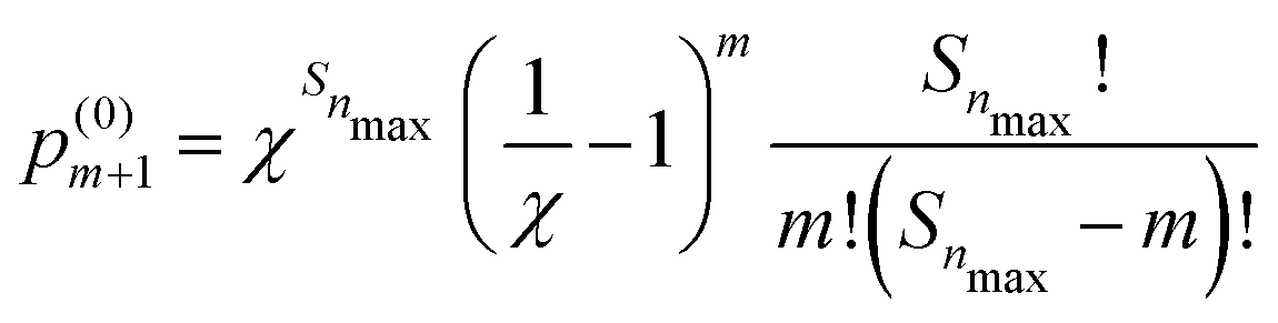 | (5) |
 is the probability of finding m′-Se (including the Se at the center) randomly placed in the nmax-sphere.
With eqn (5) we can easily evaluate the probability, p(0)m>2 that within the first three neighboring shells (i.e., in the nmax-sphere, with nmax = 3) there are more than two Se (including the Se at the center). At x = 0.45 at% the probability is p(0)m>2 = 0.8668 × 10⁻² (hereafter p(0)m will be normalized to unity, if not explicitly stated otherwise), while at x = 0.95 at% the probability is p(0)m>2 = 0.2897 × 10⁻¹. So, according to our model, within the concentration range of interest, the probability of forming (SeSi)3–VSi and (SeSi)4–VSi is less than 3%. So, we neglect the possibility of forming the complexes which involve three or four Se, and we focus on our estimation of the complexes involving one or two dopants.
In our model, the formation of a complex D having a formation energy ΔEFormD can occur at temperature T according to a probability proportional to the Boltzmann distribution, if and only if the number of dopants which are randomly placed in the nmax-sphere is equal to or greater than the number of dopants forming the complex. We re-call that p(0)m is the probability of finding m-Se randomly placed in the nmax-sphere, and, according to the above consideration, we chose for simplicity m ≤ 2. The probability of finding a defect Dn constituted by n-dopants in the nmax-sphere containing m-Se is
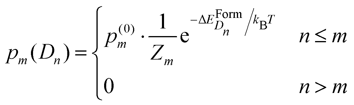 | (6) |
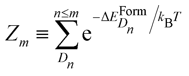 is the partition function with n that runs over all the distinct types of defects Dn with n ≤ m. The relative concentration of defect Dn is given by
 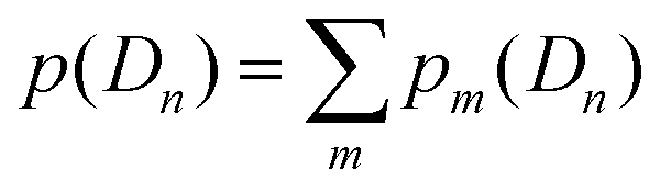 .
.
We now apply our model to evaluate the probability of different complexes within the optimal doping range for intermediate band applications, as reported in the main text.
In our estimation we choose x = 0.75 at%, nmax = 3, and m ≤ 2. For this choice of parameters, the probability to find only one Se within the nmax-sphere is p1(0) = 0.8214, while the probability of finding two Se within the nmax-sphere is p2(0) = 0.1621. The probability of finding one SeSe in a nmax-sphere containing only one random Se is obviously p1(SeSi) = p1(0), according to eqn (6). Less trivial is the case of two random Se present in the nmax-sphere. Within the nmax-sphere the two Se can arrange according to the Boltzmann distribution to the three allowed configurations: two single SeSi, or one SeSi–SeSi dimer, or one (SeSi)2–VSi complex. According to eqn (6) where  is the partition function and D ∈ [SeSi;SeSi–SeSi;(SeSi)2–VSi]. With the p(0) parameters reported above, and the formation energy reported in Table 3 we evaluate the relative concentration of the complexes: SeSi, SeSi–SeSi, (SeSi)2–VSi, the results for the relative concentration p(D) are displayed in the same table. As reported in the table, according to our model the large majority of the complexes is constituted by SeSi, and SeSi–SeSi. All other types of complexes contribute less than 3% to the relative concentration for all types of complexes.
| Complex | ΔEFormD (eV) | Concentration (%) |
|---|---|---|
| SeSi | 1.90 | 82.21 |
| (SeSi)2–VSi | 1.59 | 0.56 |
| SeSi–SeSi | 1.11 | 15.58 |
| Other complexes | — | 1.65 |
The choice of the temperature in eqn (6) is rather arbitrary. To evaluate the relative concentrations displayed in Table 3 we take T = 1687 K, i.e. equal to Si melting point, which corresponds to the maximum value that the sum of the concentration of all other complexes different from SeSi, and SeSi–SeSi can assume (within our model and the choice of the parameters different than T). For lower temperatures, T < 1687 K, the sum of the relative concentrations of all other complexes should be lower.
Therefore, to evaluate the critical concentration, xc, at which the IMT occurs, we limited ourselves to consider the SeSi, and SeSi–SeSi populations (re-normalizing the relative concentration considering only these two types of complexes). We obtained xc = 0.50 at%. The xc value is mainly determined by xM of SeSi population (xM ≃ 0.46, cn ∼ 84%) with respect to SeSi–SeSi one (xM ≃ 0.93, cn ∼ 16%). This result, reported in the main text, is quite intuitive: complexes involving three or more Se are penalized by the low probability to find three or more Se close enough to form a complex, while the formation of the complex (SeSi)2–VSi is energetically unfavored with respect to SeSi–SeSi by the higher formation energy.
To provide an intuitive, albeit approximate, picture of the mechanism involved in our model we assume that, in the silicon crystal which constitutes the experimental sample, the Se atoms have a very limited mobility, remaining close (says within a NN-distance) to the lattice sites where the Se atoms were originally located by the random distribution (obviously, the model can be generalized to include the moving to NNn lattice sites). At variance, we assume that the Si atoms have very high mobility, since the formation of Si vacancies is assumed to occur according to a Boltzmann factor. This assumption can be justified, at least in part, by the fact that a Si atom has a smaller covalent radius than a Se atom.
Appendix C: Electronic bandstructure
To prove our estimation of xM for SeSi and SeSi–SeSi, in Fig. 5 we display the bandstructure of single SeSi at x = 0.46 at%, while in Fig. 6 we display the bandstructure of SeSi–SeSi at x = 0.93 at%. The two bandstructures denote two systems very close to the semi-metallic state in which the conduction band minimum is basically equal to the maximum of the impurity band. | ||
| Fig. 5 Electronic bandstructure of Se hyperdoped Si, Si1−xSex, for single SeSe at x = 0.46 at%. The zero of the energy scale corresponds to the Fermi energy. | ||
 | ||
| Fig. 6 Electronic bandstructure of Se hyperdoped Si Si1−xSex, for SeSe–SeSe dimer at x = 0.93 at%. The zero of the energy scale corresponds to the Fermi energy. | ||
For completeness, by using the same Se concentration we computed the DOS displayed in Section III.B, for each type of defect we provide the electronic bandstructure, along high symmetry direction in the Brillouin zone (labels along high symmetry directions the Brillouin zone has been assigned according to the symmetry of the super-cell used in the simulation, see Appendix A for further details).
In Fig. 7 we display, the electronic bandstructure of SeSi–SeSi for x = 0.463 at%. At variance with bandstructure of the same complex for x = 0.93 at% displayed in Fig. 6, at the lower concentration of x = 0.463 at%, the IB is still separated by the conduction band.
 | ||
| Fig. 7 Electronic bandstructure of Se hyperdoped Si, Si1−xSex, for substitutional SeSi–SeSi dimer at x = 0.463 at%. The zero of the energy scale corresponds to the Fermi energy. | ||
In Fig. 8 we display the electronic bandstructure of Se interstitials. For ISe in the tetrahedral position we can notice the partially filled IB, which is situated deep in the bandgap, thus acting as an acceptor defect. At variance, at the considered concentration, the IB of ISe in hexagonal position, is merged into the conduction band, as can be noticed by looking at the bandstructure along the Γ–X direction in the Brillouin zone.
 | ||
| Fig. 8 Electronic bandstructure of Se hyperdoped Si, Si1−xSex, for Se interstitial, ISe, in tetrahedral (top panel) and hexagonal position (bottom panel) at x = 0.461 at%. The zero of the energy scale corresponds to the Fermi energy. | ||
In Fig. 9 and 10 we display the electronic bandstructure of the complexes (SeSi)m–VSi, m = 1, 2, 3, and 4. As discussed in the main text, at x ≃ 0.465 at%, the (SeSi)1–VSi is an acceptor complex, and it is characterized by a partially filled IB in the middle of the gap. At variance at x ≃ 0.438 at%, the IB of (SeSi)3–VSi is fully merged into the conduction band. As can be noticed by looking at the figures, the considered concentrations (SeSi)2–VSi and (SeSi)4–VSi have shallow IBs, and these complexes act as donors. The bandstructures illustrated above provide a complementary picture of the analysis of electronic properties of the different types of defects discussed in Section III.B by means of the DOS.
 | ||
| Fig. 9 Electronic bandstructure of Se hyperdoped Si, Si1−xSex, for (SeSi)1–VSi at x ≃ 0.465 at% (top panel), and for (SeSi)2–VSi at x ≃ 0.464 at% (bottom panel). The zero of the energy scale corresponds to the Fermi energy. | ||
 | ||
| Fig. 10 Electronic bandstructure of Se hyperdoped Si, Si1−xSex, for (SeSi)3–VSi at x ≃ 0.438 at% (top panel), and for (SeSi)4–VSi at x ≃ 0.463 at% (bottom panel). The zero of the energy scale corresponds to the Fermi energy. | ||
Appendix D: Formation energy of a couple of substitutional Se
To support the assumption of a random distribution of Se dopants at the different lattice sites of silicon, used in Appendix B to provide a quantitative estimation of the concentration of the different types of defects, we considered the formation energy of a couple of SeSi placed at different distances at the substitutional sites of Si. The results for x = 0.93 at% are displayed in Fig. 11. We considered the first Se placed at a substitutional site in the Si lattice site, while the second Se is placed at a substitutional site in one of the neighbouring shells of the Si lattice that surrounds the first Se. We considered an increasing number of next nearest neighbour shells NNn, n = 1, 2,…,6. We recall that n = 1 corresponds to the SeSi–SeSi (with the substitutional Se in a nearest neighbour shell). The lowest formation energy corresponds to the SeSi–SeSi dimer, while all the other energies are comparable to the one of single SeSi at the same concentration (see Fig. 1). | ||
| Fig. 11 Formation energy (per atom) of a couple of Se substitutional impurities in Se hyperdoped Si, Si1−xSexi, at x = 0.93 at%. One Se is placed at the n-neighbour shells (NNn, n = 1, 2,…,6) surrounding the other Se. Se–Se distance refers to relaxed positions and increases according to the increasing shell number n. Dashed line is a guide for the eye. | ||
From the figure we can conclude that while the dimer formation is energetically favored (probably due to the similar Se–Se bond length in the Se2 molecule with the Si–Si bond length in bulk Si, see also Section 3.2) the positioning of Se at the other lattice sites can be considered, with a good approximation, equally probable, due to the very similar formation energies, thus justifying a distribution with equal probability of SeSi at this lattice site.
Acknowledgements
We acknowledge the CINECA for computer resources allocated under the ISCRA initiative (IMeCS project), and R. Colnaghi for technical support on computer hardware.References
- S. Hu, P. Han, S. Wang, X. Mao, X. Li and L. Gao, Improved photoresponse characteristics in se-doped si photodiodes fabricated using picosecond pulsed laser mixing, Semicond. Sci. Technol., 2012, 27, 102002 CrossRef.
- Y. Berencén, S. Prucnal, F. Liu, I. Skorupa, R. Huebner, L. Rebohle, S. Zhou, H. Schneider, M. Helm and W. Skorupa, Room-temperature short-wavelength infrared si photodetector, Sci. Rep., 2017, 7, 43688 CrossRef PubMed.
- M. Wang and Y. A. Berencén, Room-temperature infrared photoresponse from ion beam-hyperdoped silicon, Phys. Status Solidi A, 2021, 218, 2000260 CrossRef CAS.
- A. Luque, A. Marti and C. Stanley, Understanding intermediate-band solar cells, Nat. Photonics, 2012, 6, 146 CrossRef CAS.
- Y. Okada, N. J. Ekins-Daukes, T. Kita, R. Tamaki, M. Yoshida, A. Pusch, O. Hess, C. C. Phillips, D. J. Farrell, K. Yoshida, N. Ahsan, Y. Shoji, T. Sogabe and J. F. Guillemoles, Intermediate band solar cells: recent progress and future directions, Appl. Phys. Rev., 2015, 2(2), 021302 Search PubMed.
- M. Wang, A. Debernardi, Y. Berencén, R. Heller, C. Xu, Y. Yuan, Y. Xie, R. Bottger, L. Rebohle, W. Skorupa, M. Helm, S. Prucnal and S. Zhou, Breaking the doping limit in silicon by deep impurities, Phys. Rev. Appl., 2019, 11, 054039 CrossRef CAS.
- International Technology Roadmap for Semiconductors (ITRS), Tech. Rep. (Semiconductor Industry Association).
- H.-J. Gossmann, C. S. Rafferty and P. Keys, Junctions for deep sub-100 nm mos: How far will ion implantation take us?, J. Mater. Res. Soc. Symp., 2000, 610, B1.2.1–B1.2.10 Search PubMed.
- H. Gossmann, F. C. Unterwald and H. S. Luftman, Doping of si thin films by lowtemperature molecular beam epitaxy, J. Appl. Phys., 1993, 73, 8237 CrossRef CAS.
- H. H. Radamson, M. R. Sardela Jr, L. Hultman and G. V. Hansson, Characterization of highly sbdoped si using highresolution xray diffraction and transmission electron microscopy, J. Appl. Phys., 1994, 76, 763 CrossRef CAS.
- K. Saarinen, J. Nissila, H. Kauppinen, M. Hakala, M. Puska, P. Hautojarvi and C. Corbel, Identification of vacancy-impurity complexes in highly n-type si, Phys. Rev. Lett., 1999, 82, 1883 CrossRef CAS.
- V. Ranki, K. Saarinen, J. Fage-Pedersen, J. Hansen and A. Larsen, Electrical deactivation by vacancy-impurity complexes in highly as-doped si, Phys. Rev. B: Condens. Matter Mater. Phys., 2003, 67, 041201 CrossRef.
- M. Rummukainen, I. Makkonen, V. Ranki, M. J. Puska, K. Saarinen and H. J. L. Gossmann, Vacancy-impurity complexes in highly sb-doped si grown by molecular beam epitaxy, Phys. Rev. Lett., 2005, 94, 165501 CrossRef CAS PubMed.
- M. Ramamoorthy and S. Pantelides, Complex dynamical phenomena in heavily arsenic doped silicon, Phys. Rev. Lett., 1996, 76, 4753 CrossRef CAS PubMed.
- D. Mueller, E. Alonso and W. Fichtner, Arsenic deactivation in si: Electronic structure and charge states of vacancy-impurity clusters, Phys. Rev. B: Condens. Matter Mater. Phys., 2003, 68, 045208 CrossRef.
- A. Satta, E. Albertazzi, G. Lulli and L. Colombo, Ab initio structures of asmv complexes and the simulation of rutherford backscattering channeling spectra in heavily as-doped crystalline silicon, Phys. Rev. B: Condens. Matter Mater. Phys., 2005, 72, 235206 CrossRef.
- D. Mathiot and J. C. Pfister, Diffusion of arsenic in silicon: validity of the percolation model, Appl. Phys. Lett., 1983, 42, 1043–1044 CrossRef CAS.
- D. Mathiot and J. C. Pfister, Dopant diffusion in silicon: a consistent view involving nonequilibrium defects, J. Appl. Phys., 1984, 55, 3518 CrossRef CAS.
- K. Pandey, A. Erbil, G. Cargill, R. Boehme and D. Vanderbilt, Annealing of heavily arsenic-doped silicon: Electrical deactivation and a new defect complex, Phys. Rev. Lett., 1988, 61, 1282–1285 CrossRef CAS PubMed.
- D. Lawther, U. Myler, P. Simpson, P. Rousseau, P. Griffin and J. Plummer, Vacancy generation resulting from electrical deactivation of arsenic, Appl. Phys. Lett., 1995, 67, 3575–3577 CrossRef CAS.
- V. Ranki, J. Nissila and K. Saarinen, Formation of vacancy-impurity complexes by kinetic processes in highly as-doped si, Phys. Rev. Lett., 2002, 88, 105506 CrossRef CAS PubMed.
- V. Ranki and K. Saarinen, Formation of thermal vacancies in highly as and p doped si, Phys. Rev. Lett., 2004, 93, 255502 CrossRef CAS PubMed.
- R. Pinacho, M. Jaraiz, P. Castrillo, I. Martin-Bragado, J. Rubio and J. Barbolla, Modeling arsenic deactivation through arsenic-vacancy clusters using an atomistic kinetic monte carlo approach, Appl. Phys. Lett., 2005, 86, 252103 CrossRef.
- P. Voyles, D. Muller, J. Grazul, P. Citrin and H. Gossmann, Atomic-scale imaging of individual dopant atoms and clusters in highly n-type bulk si, Nature, 2002, 416, 826 CrossRef CAS PubMed.
- D. Mueller and W. Fichtner, Highly n-doped silicon: Deactivating defects of donors, Phys. Rev. B: Condens. Matter Mater. Phys., 2004, 70, 245207 CrossRef.
- D. Chadi, P. Citrin, C. Park, D. Adler, M. Marcus and H. Gossmann, Fermi-level-pinning defects in highly n-doped silicon, Phys. Rev. Lett., 1997, 79, 4834 CrossRef CAS.
- M. T. Winkler, D. Recht, M.-J. Sher, A. J. Said, E. Mazur and M. J. Aziz, Insulator-to-metal transition in sulfur-doped silicon, Phys. Rev. Lett., 2011, 106, 178701 CrossRef PubMed.
- E. Ertekin, M. T. Winkler, D. Recht, A. J. Said, M. J. Aziz, T. Buonassisi and J. C. Grossman, Insulator-to-metal transition in selenium-hyperdoped silicon: Observation and origin, Phys. Rev. Lett., 2012, 108, 026401 CrossRef PubMed.
- M. Wang, A. Debernardi, W. Zhang, C. Xu, Y. Yuan, Y. Xie, Y. Berencén, S. Prucnal, M. Helm and S. Zhou, Critical behavior of the insulator-to-metal transition in Te-hyperdoped si, Phys. Rev. B: Condens. Matter Mater. Phys., 2020, 102, 085204 CrossRef CAS.
- K. Suzuki, Y. Tada, Y. Kataoka, K. Kawamura, T. Nagayama, S. Nagayama, C. W. Magee, T. H. Bueyueklimanli, D. C. Mueller, W. Fichtner and C. Zechner, Maximum active concentration of ion-implanted phosphorus during solid-phase epitaxial recrystallization, IEEE Trans. Electron Devices, 2007, 54, 1985 CAS.
- Z.-Y. Zhao and P.-Z. A. Yang, Insight into insulator-to-metal transition of sulfur-doped silicon by dft calculations, Phys. Chem. Chem. Phys., 2014, 16, 17499 RSC.
- S. Zhou, F. Liu, S. Prucnal, K. Gao, M. Khalid, C. Baehtz, M. Posselt, W. Skorupa and M. K. Helm, Hyperdoping silicon with selenium: solid vs. liquid phase epitaxy, Sci. Rep., 2015, 5, 8329 CrossRef CAS PubMed.
- F. Liu, S. Prucnal, Y. Berencen, Z. Zhang, Y. Yuan, Y. Liu, R. Heller, R. Boettger, L. Rebohle, W. Skorupa, M. Helm and S. Zhou, Realizing the insulator-to-metal transition in se-hyperdoped si via non-equilibrium material processing, J. Phys. D: Appl. Phys., 2017, 50, 415102 CrossRef.
- See e.g. H. Overhof, M. Scheffler and C. M. Weinert, Formation energies, electronic structure, and hyperfine fields of chalcogen point defects and defect pairs in silicon, Phys. Rev. B: Condens. Matter Mater. Phys., 1991, 43, 12494 CrossRef CAS PubMed , and references therein.
- P. Giannozzi, S. Baroni, N. Bonini, M. Calandra, R. Car, C. Cavazzoni, D. Ceresoli, G. L. Chiarotti, M. Cococcioni, I. Dabo, A. D. Corso, S. Fabris, G. Fratesi, S. de Gironcoli, R. Gebauer, U. Gerstmann, C. Gougoussis, A. Kokalj, M. Lazzeri, L. Martin-Samos, N. Marzari, F. Mauri, R. Mazzarello, S. Paolini, A. Pasquarello, L. Paulatto, C. Sbraccia, S. Scandolo, G. Sclauzero, A. P. Seitsonen, A. Smogunov, P. Umari and R. M. Wentzcovitch, Quantum espresso: a modular and open-source software project for quantum simulations of materials, J. Phys.: Condens. Matter, 2009, 21, 395502 CrossRef PubMed.
- A. M. Rappe, K. M. Rabe, E. Kaxiras and J. D. Joannopoulos, Optimized pseudopotentials, Phys. Rev. B: Condens. Matter Mater. Phys., 1990, 41, 1227(R) CrossRef PubMed.
- D. Vanderbilt, Soft self-consistent pseudopotentials in a generalized eigenvalue formalism, Phys. Rev. B: Condens. Matter Mater. Phys., 1990, 41, 7892(R) CrossRef PubMed.
- L. Kleinmann and D. Bylander, Efficacious form for model pseudopotentials, Phys. Rev. Lett., 1982, 48, 1425 CrossRef.
- J. P. Perdew, K. Burke and M. Ernzerhof, Generalized gradient approximation made simple, Phys. Rev. Lett., 1996, 77, 3865 CrossRef CAS PubMed; J. P. Perdew, K. Burke and M. Ernzerhof, Generalized gradient approximation made simple, Phys. Rev. Lett., 1997, 78, 1396(E) CrossRef.
- R. W. Wyckoff, Crystal Structures, Wiley Interscience Publication, New York, 1971, vol. 1 Search PubMed.
- H. J. Monkhorst and J. D. Pack, Special points for brillouinzone integration, Phys. Rev. B: Condens. Matter Mater. Phys., 1976, 13, 5188 CrossRef.
- G. Petretto, A. Debernardi and M. Fanciulli, Confinement effects and hyperfine structure in se doped silicon nanowires, Nano Lett., 2011, 11, 4509 CrossRef CAS PubMed.
| This journal is © the Owner Societies 2021 |