
Transient absorption measurements of interlayer charge transfer in a WS2/GeS van der Waals heterostructure
Lier
Deng
 a,
Weihang
Yuan
a,
Dawei
He
b,
Shuangyan
Liu
b,
Yuxuan
Du
a,
Lei
Gong
a and
Huan
Liu
*a
a,
Weihang
Yuan
a,
Dawei
He
b,
Shuangyan
Liu
b,
Yuxuan
Du
a,
Lei
Gong
a and
Huan
Liu
*a
aSchool of Optoelectronic Engineering, Xi’an Technological University, Xi’an 710032, China. E-mail: liuhuan@xatu.edu.cn
bKey Laboratory of Luminescence and Optical Information, Ministry of Education, Institute of Optoelectronic Technology, Beijing Jiaotong University, Beijing 100044, China
First published on 11th July 2021
Abstract
We introduce germanium sulfide (GeS) as a new layered material for the fabrication of two-dimensional van der Waals materials and heterostructures. Heterostructures of WS2/GeS were fabricated using mechanical exfoliation and dry transfer techniques. Significant photoluminescence quenching of WS2 in the heterostructures indicates efficient charge transfer. Transient absorption measurements were performed to study the dynamics of charge transfer. The results show that the heterostructure forms a type-II band alignment with the conduction band minimum and valence band maximum located in the WS2 and GeS layers, respectively. The ultrafast hole transfer from WS2 to GeS is confirmed by the faster decay of the lower peak value of the differential reflection signal in the heterostructure sample, in comparison to the WS2 monolayer. These results introduce GeS as a promising semiconductor material for developing new novel heterostructures.
Introduction
Two-dimensional (2D) materials exist in layered structures, in the form of stacks of strongly bonded layers with weak interlayer attraction, which allows exfoliation into individual and atomically thin layers.1 Many 2D materials have excellent electronic and optical properties; the most typical ones include graphene, transition metal dichalcogenides (TMDs), phosphorene and graphene analogues such as arsenene and antimonene.2–6 Graphene has excellent properties such as high conductivity, wide absorption band and high mechanical strength.7,8 However, its lack of a band gap is a limiting factor in some electronic and optoelectronic applications, such as using it as the channel material for field-effect transistors.9 The band gap range of TMDs extends from visible light to the near-infrared band;10–14 however, the charge mobility of these materials is several orders of magnitude lower than that of graphene.15,16 Low carrier mobility makes it difficult to improve the response speed of TMD-based optoelectronic devices. Phosphorene presents an in-plane anisotropic response to external stimulations, which brings new elements to the study of 2D materials.17,18 However, due to the existence of lone-pair electrons, phosphorene is prone to oxidation and decomposition in the ambient environment, which presents a challenge for developing phosphorene based devices.Although the 2D material library is rapidly increasing, no single 2D material can perfectly meet all the requirements for practical applications.19,20 van der Waals (vdW) heterostructures, which break the limitation of the restricted properties of single materials, are attractive prospects for designing new devices with tailored properties.21–23 VdW heterostructures are very different from the traditional 3D semiconductor heterostructures, as each layer acts simultaneously as the bulk material and the interface, which reduces the amount of charge displacement in each layer. At present, the research on vdW heterostructures mainly focuses on graphene/TMD, graphene/phosphorene, TMD/TMD, and TMD/phosphorene. Searching for new 2D materials, preferably with new optoelectronic properties, to expand the library of vdW heterostructures is highly desirable.
In this work, we introduce a new 2D material to the library of vdW heterostructures, GeS. The family of monolayer group-IV monochalcogenides (MXs), including GeS, GeSe, SnS, and SnSe, has similar puckered and cellular structures to phosphorene. They are a series of 2D semiconductors with many intriguing properties, such as excellent performance in optoelectronics, photovoltaics and ferroelectricity.24 Consisting of two elements makes MXs possess different electronegativity from phosphorene, which lacks centro-symmetry.25 For example, MXs present two orders of magnitude higher piezoelectric coefficients than MoS2 and h-BN.26,27 They also have an ultra-high thermoelectric figure of merit and the potential for realizing topological crystal insulators as sensor materials. Among these single-layer IV–VI compounds, GeS is regarded as a promising material for high-efficiency photodetectors and solar cells with high sensitivities and external quantum efficiencies, as suggested by recent theoretical and experimental studies.28–30
A bulk GeS crystal consists of double-layer slabs of Ge–S in a zigzag configuration, which are bonded by vdW interactions with an interlayer separation of 3.5 Å as shown in Fig. 1(a). At room temperature, its thermodynamically preferred phase is the orthorhombic α-GeS structure (a = 10.47 Å, b = 3.64 Å, c = 4.3 Å).31,32 The original unit cell of the GeS monolayer (ML) contains eight atoms, four of each type, arranged as shown in Fig. 1(b). Based on density functional theory (DFT) calculations, the GeS monolayer is a semiconductor with an indirect band gap of 2.34 eV. Its electron mobility is 3680 cm2 V−1 s−1, which is much higher than that of the MoS2 monolayer and silicene.33,34 Besides, Zhang et al. found, using theoretical calculations, that monolayer GeS is stable in the ambient environment because there are no soft phonon modes in its phonon spectrum.35 Experimentally, GeS nanosheets have recently been fabricated using solution-phase synthesis or vapor deposition processes.36,37 The smallest thickness achieved so far is 2 MLs by liquid phase exfoliation.38
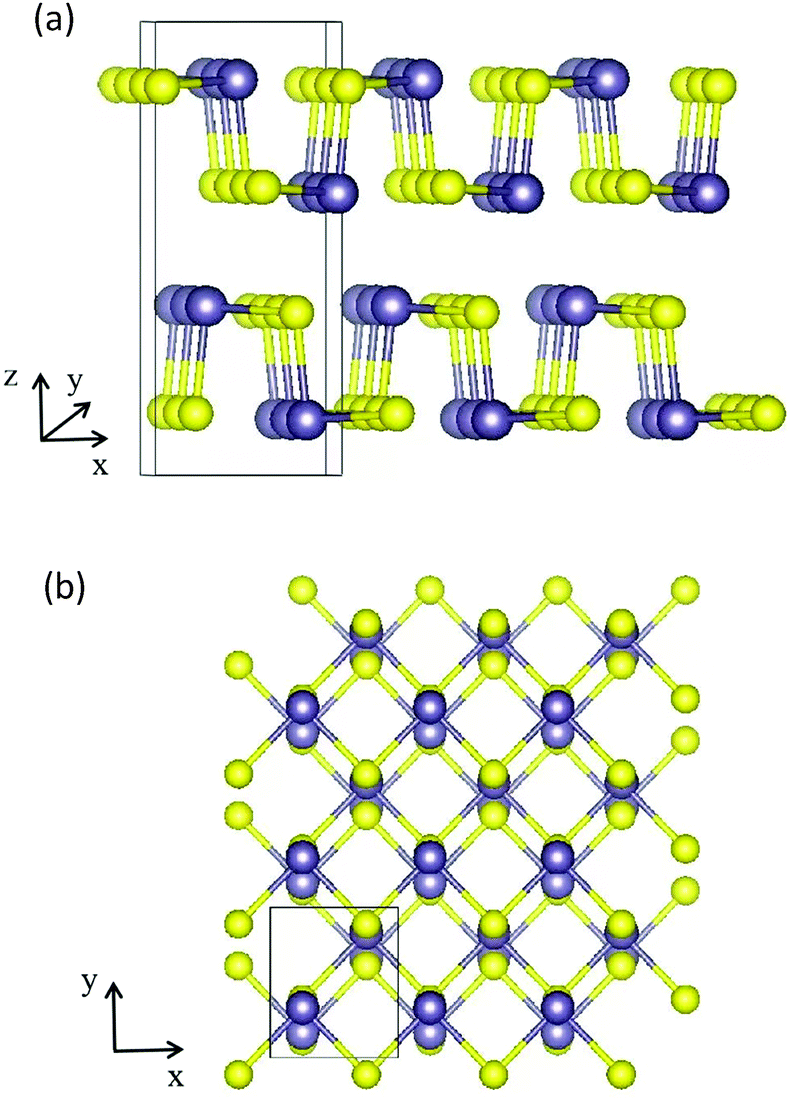 | ||
| Fig. 1 (a) Side view along the y direction of a bulk GeS crystal. (b) Top view of the atomic structure of the GeS monolayer, the purple and yellow balls represent Ge and S atoms, respectively. | ||
Despite increasing studies on GeS as a new 2D material, its inclusion in vdW heterostructures has only been speculated theoretically. Based on first-principles calculations, Wang et al. presented the control of the electronic properties of GeS/phosphorene heterostructures by thickness.39 Zhu et al. predicted that GeS/FeCl2 heterostructures had potential applications in spintronic devices because of their tunable electronic band structure and magnetic anisotropy.40 Furthermore, strain and electric field control of the electronic properties in SiP(SiAs)/GeS and the band alignment tuning in GeS/arsenene heterostructures have been discussed theoretically.41,42 Hence, experimental studies of GeS-based vdW heterostructures are highly desired as they can validate the feasibility of its integration with other 2D materials. In particular, combining GeS with TMDs, the most extensively studied 2D materials to date, would be of high interest.
In this work, we fabricated a vdW heterostructure formed by monolayer WS2 and multilayer GeS. Transient absorption measurements were performed to study the dynamics of charge transfer between the two materials. We found that monolayer WS2 and multilayer GeS form a type-II band alignment. Our transient absorption measurements indicate that charge transfer from WS2 to GeS occurs on a subpicosecond time scale. These results provide useful information for developing TMDs/MX heterostructures for various applications.
Experimental
The WS2/GeS heterostructure sample used in this study was fabricated by mechanical exfoliation and dry transfer. First, GeS multilayer flakes were cleaved from the fresh surface of a GeS crystal using an adhesive tape and transferred to a Si/SiO2 (90 nm) substrate. Second, a large number of flakes containing monolayers were exfoliated similarly from a WS2 crystal and transferred to a flexible polydimethylsiloxane (PDMS) substrate. Next, under an optical microscope, a monolayer WS2 flake was transferred onto the GeS flake to form a WS2/GeS heterostructure. Finally, the sample was annealed for 2 hours at 200 °C in a 100-sccm Ar gas environment at a base pressure of 2–3 Torr.The photocarrier dynamics in the WS2/GeS heterostructure and monolayer WS2 was studied by transient absorption measurement.43Fig. 2 shows schematically the home-made setup used in this study. An 80 MHz mode-locked Ti:sapphire laser pumped using a 532 nm diode laser produces 100 fs pulses with a central wavelength of 790 nm. This beam was divided into two parts by a beamsplitter. One part was sent to an optical parametric oscillator to generate a tunable signal output with a central wavelength in the range of 490–750 nm, serving as the probe. The other part was sent to a beta barium borate (BBO) crystal to generate its second harmonic at 395 nm, serving as the pump. The pump and probe beams were combined using a beamsplitter and focused on the sample surface through a microscope objective lens with spot size of about 2 μm full width at half maximum. The reflected probe was sent to a silicon photodiode, whose output was measured by a lock-in amplifier. Color filters were used to prevent the pump light from reaching the photodiode. The photocarrier dynamics was revealed by detecting the pump-induced relative change of the probe reflection (differential reflectance), ΔR/R0 = (R − R0)/R0, where R and R0 are the probe reflectance of the sample with and without the presence of the pump. The intensity of the pump reaching the sample was modulated at 2 KHz using a mechanical chopper, which was placed in the pump arm. A linear motor stage was used to control the path length of the pump arm, and thus the arrival time of the pump pulse. We define the probe delay as the arrival time of the probe pulse at the sample with respect to the pump pulse. The differential reflectance ΔR/R0 was measured as a function of the probe delay.
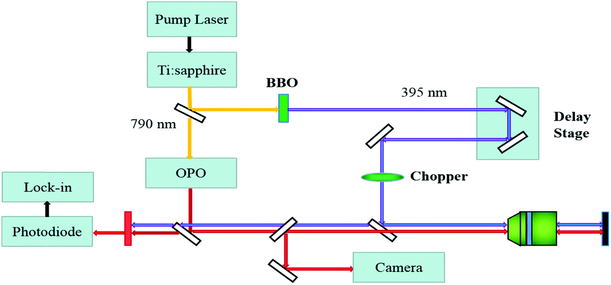 | ||
| Fig. 2 Schematic of the transient absorption microscope setup. | ||
Results and discussion
Fig. 3(a) shows an optical microscope image of a WS2/GeS heterostructure sample with an area of nearly 200 square micrometers, which is large enough for the photoluminescence (PL) and transient absorption measurements. Fig. 3(b) shows the PL spectra of the monolayer WS2 (red) and the WS2/GeS heterostructure (black) regions under the excitation of a 405 nm continuous-wave laser with an incident power of 3 μW and a spot size of about 2 μm full width at half maximum. The PL peak position of the monolayer WS2 region (612 nm) is consistent with the previously reported values.44 The PL of WS2 in the heterostructure (black curve) is much lower than that of the individual WS2 ML. A quenching of about 96% indicates that most excited electrons or holes (or both) transfer from WS2 to GeS before their recombination in WS2. There is a small shift of about 7 nm between the two peaks, which originates from the different dielectric environments in the heterostructure compared to the individual WS2 ML. Fig. 3(c) illustrates the predicted band alignment of the heterostructure, where the upper and lower boxes represent the conduction and valence bands of WS2 and GeS, respectively. The numbers show the energy of the conduction band minimum (CBM) and valence band maximum (VBM) with respect to the vacuum level, according to theoretical results.39,45 As shown, WS2 and GeS are expected to form a type-II heterostructure with the CBM and VBM located in the WS2 and GeS layers, respectively. Hence, electrons excited in GeS are expected to transfer to WS2, driven by the potential offset, while holes excited in WS2 would transfer to GeS to lower their potential energy. This charge transfer driven by the band offset in type-II heterostructures has been previously discussed.46–48 In our PL measurements, since the holes excited in WS2 transfer to GeS, instead of forming excitons and recombining in WS2, we observed the quenching of the WS2 PL peak in the heterostructure.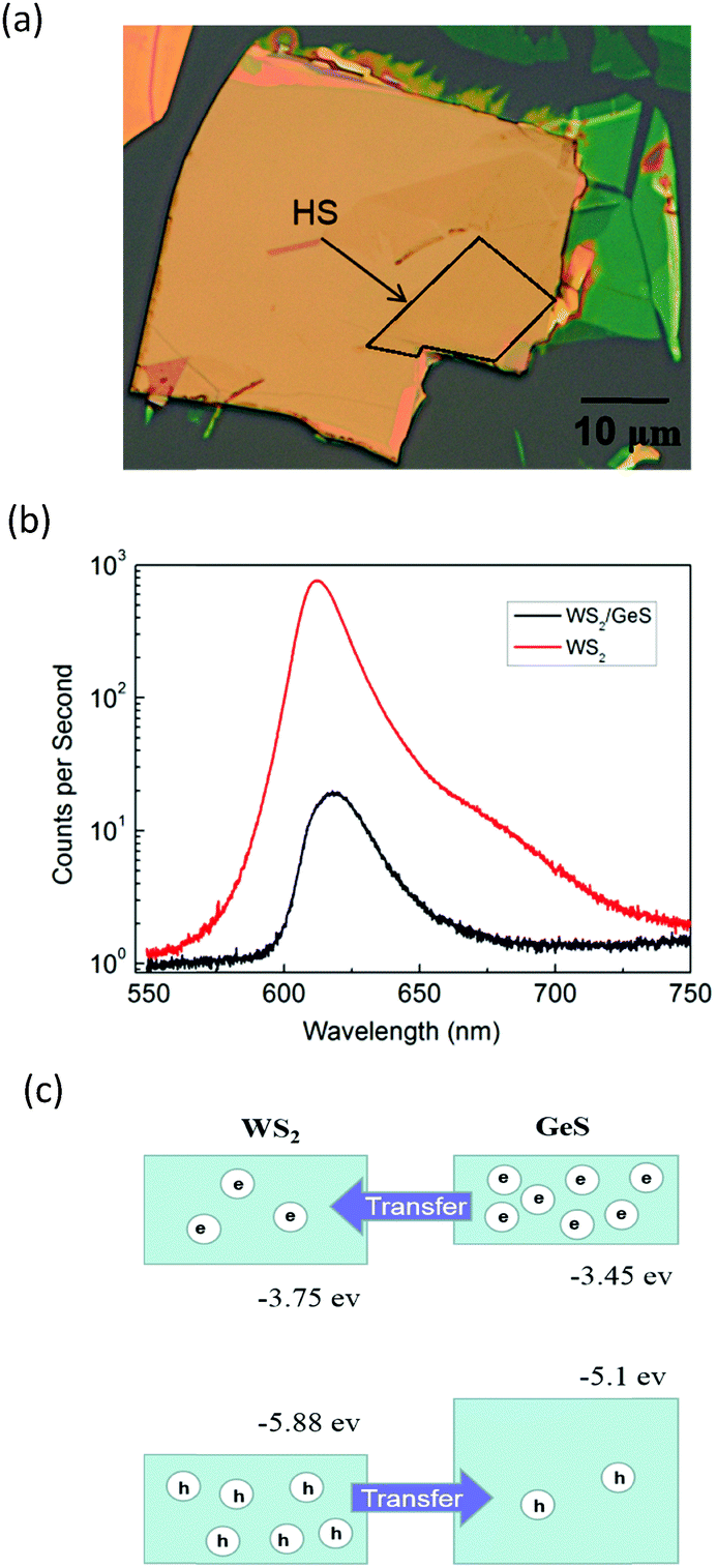 | ||
| Fig. 3 (a) Optical microscope image of the WS2/GeS heterostructure; the heterostructure is in the black box. (b) Photoluminescence spectra of the samples measured from the regions of monolayer WS2 (red) and the heterostructure (black). (c) The predicted band alignment of the WS2/GeS heterostructure. | ||
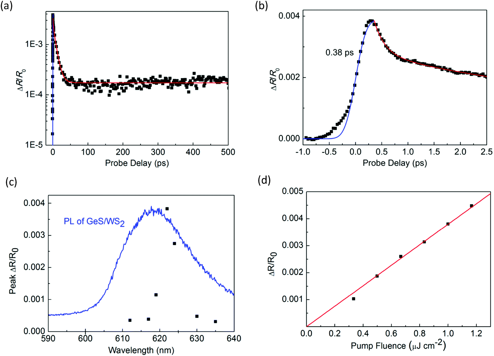
In the transient absorption measurements, we first investigated the individual monolayer WS2 using a 395 nm pump pulse with an incident energy fluence of Fi = 1 μJ cm−2. According to Beer's law, the transmitted fluence can be calculated by the equation Ft = Fiexp(−αL), where α and L represent the absorption coefficient and thickness of the WS2 ML, respectively. Hence, we can get the absorbed fluence Fa = Fi[1 − exp(−αL)], and for αL ≪ 1, Fa ≈ FiαL. Based on the assumption that every absorbed photon excites one electron–hole pair, the injected carrier density is N = Fa/(ħw) = FiαL/(ħw), where ħw is the photon energy. Using α = 2.3 × 10⁸ m−1 and L = 0.7 nm49 the estimated peak carrier density is 3.2 × 10¹¹ m−1. A 617 nm probe pulse is tuned to the exciton resonance of the WS2 ML. The differential reflectance of this pulse, which was measured as a function of the probe delay, is shown in Fig. 4 for long [Fig. 4(a)] and short time ranges [Fig. 4(b)]. The rise of the signal is rather fast, which can be fit by the integral of a Gaussian function with a full width at half maximum of 0.38 ps, as indicated by the blue curve over the data points in Fig. 4(b). This time is close to the cross-correlation of the pump and probe pulse, which indicates that the injected carriers produce a peak differential reflectance signal instantaneously, as has been generally observed in TMD monolayers and has been attributed to the ultrafast thermalization and relaxation of photocarriers in such materials.50,51 The decay of the signal can be fit using a triple exponential function ΔR/R0 = A0 + A1e−t/τ1 + A2e−t/τ2 + A3e−t/τ3, as shown by the red curve over the data points in Fig. 4(a). The three decay constants (and their relative weights in the total signal) are 0.94 ± 0.05 (24%), 10.7 ± 0.3 (61%), and 67 ± 4 (13%), in which a constant term accounts for 2% of the total signal. The sub-picosecond decay can be attributed to the formation of excitons from the injected electron–hole pairs.52–54 The 10.7 ps and 67 ps decay processes reflect the dynamics of excitons in WS2 and are reasonably consistent with previous studies.55 The 2% background could be induced by carriers trapped at the defect states.
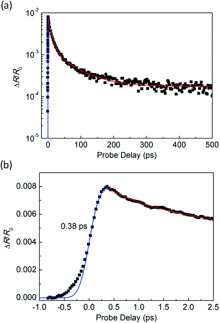 | ||
| Fig. 4 Differential reflection signal from monolayer WS2 measured using 395 nm pump and 617 nm probe pulses over (a) long and (b) short-time ranges. The red curve is a fit of the decay process by a triple exponential function. The blue curve represents the integral of a Gaussian function with a full width at half maximum of 0.38 ps. | ||
Next, we performed transient absorption measurements to study the carrier transfer in the WS2/GeS heterostructure. A 395 nm pump pulse with a peak fluence of 1 μJ cm−2 was used to excite the heterostructure sample. As theoretically predicted in Fig. 3(c), holes are expected to transfer from WS2 to GeS, driven by the potential energy offset. By using a 612 nm probe pulse, we monitor the differential reflectance of the sample, as shown by the black symbols in Fig. 5(a). We find that the peak signal from the heterostructure is about half of that from the WS2 ML. The increase of the signal is also ultrafast, as indicated by the blue curve in Fig. 5(b). The decay of the signal is also fit using the triple exponential function, as shown by the red curve. The deduced decay time constants (and their relative weights) are 0.13 ± 0.02 ps (69%), 1.3 ± 0.5 ps (4%), and 8.4 ± 0.5 ps (22%), with a constant of about 5%.
 | ||
| Fig. 5 Differential reflection signal from the WS2/GeS heterostructure measured with 395 nm pump and 617 nm probe pulses over (a) long and (b) short-time ranges. The red curve is a fit of the decay process by a triple exponential function. The blue curve represents the integral of a Gaussian function with a full width at half maximum of 0.38 ps. (c) Peak differential reflection signal from the heterostructure as a function of the pump wavelength (black squares) and the PL spectrum of the WS2 (blue curve). (d) Peak differential reflection (black squares) as a function of the pump fluence. The red line is a linear fit. | ||
The dramatically different dynamics observed for the heterostructure sample provides convincing evidence of charge transfer between WS2 and GeS. If charge transfer was absent, one would expect the dynamics from the two samples to be identical. Overall, the decay of the signal from the heterostructure is shorter than that from the WS2 monolayer. In particular, the majority of the signal (73%) decays on the 0.13 to 1.3 ps time scales. This result shows that GeS provides a fast decay channel for the photocarriers in WS2. Along with the predicted type-I band alignment, we attribute this decay to the transfer of holes from WS2 to GeS, which reduces the carrier population in WS2. This conclusion is also consistent with the PL quenching observed in the heterostructure sample. The 8.4 ps process could be due to the exciton dynamics inside WS2 that originates from regions of the sample with poor interfacial quality, which blocks charge transfer. The 5% constant could indicate the long lifetime of electrons in WS2 after the holes are transferred to GeS. Previously, interlayer charge transfer in various heterostructures has been studied using density functional theory.56–58 However, we are not aware of such studies on WS2/GeS yet. Our experimental funding could encourage more computational studies of this promising heterostructure.
To further confirm that the observed differential reflection signal originates from the WS2 layer of the heterostructure, we studied the dependence of the signal on the probe wavelength. As shown in Fig. 5(c), the peak of the signal depends strongly on the probe wavelength, which is consistent with the WS2 PL peak as shown by the blue curve. This result proves that the differential reflection signal is indeed from the exciton resonance of WS2. In the measurement shown in Fig. 5(a), the pump pulse fluence is 1 μJ cm−2, which is the same as that in the measurement of monolayer WS2 shown in Fig. 3. By repeating the measurement with different pump fluences, we find that the peak of the signal is proportional to the pump fluence, as shown in Fig. 5(d). This shows that the pump fluence of 1 μJ cm−2 used in our measurement is in the unsaturated absorption regime of WS2, which satisfies the basic assumption of the transient absorption measurement.
Conclusions
We have studied charge transfer in a WS2/GeS heterostructure by transient absorption measurements. Our experimental results are consistent with the predicted type-II band alignment of this heterostructure. We conclude that holes injected in WS2 can transfer to GeS on an ultrafast time scale based on three experimental observations in the WS2/GeS heterostructure sample in comparison to the WS2 monolayer: the PL quenching, the faster decay of the differential reflection signal, and the lower peak differential reflection signal. Hence, our study shows that GeS can be integrated with TMDs to form vdW heterostructures with superior charge transfer properties. Since GeS has attractive optoelectronic and ferroelectric properties and is environmentally friendly, earth-abundant, and low-cost, its inclusion brings promise for developing new novel vdW heterostructures.Conflicts of interest
There are no conflicts of interest to declare.Acknowledgements
We are grateful for the financial support from the Key Research and Development Program of Shaanxi Province (Grant No. 2019ZDLGY16-01), the Beijing Natural Science Foundation (Grant No. Z190006), the National Natural Science Foundation of China (Grant No. 61527817, 61875236, 61905010, and 61975007), and the Scientific Research Program funded by Shaanxi Provincial Education Department (Grant No. 20JS059).References
- K. S. Novoselov, A. K. Geim, S. V. Morozov, D. Jiang, Y. Zhang, S. V. Dubonos, I. V. Grigorieva and A. A. Firsov, Science, 2004, 306, 666–669 CrossRef CAS PubMed.
- Z. Cui, X. Wang, Y. C. Ding, E. L. Li, K. F. Bai, J. S. Zheng and T. Liu, Appl. Surf. Sci., 2020, 530, 147275 CrossRef CAS.
- M. L. Sun and U. Schwingenschlögl, Adv. Energy Mater., 2021, 11, 2003633 CrossRef CAS.
- S. Wang, F. R. Pratama, M. S. Ukhtary and R. Saito, Phys. Rev. B, 2020, 101, 081414 CrossRef CAS.
- M. L. Sun and U. Schwingenschlögl, Chem. Mater., 2020, 32, 4795–4800 CrossRef CAS.
- S. Wang, M. S. Ukhtary and R. Saito, Phys. Rev. Res., 2020, 2, 033340 CrossRef CAS.
- S. D. Sarma, S. Adam, E. H. Hwang and E. Rossi, Rev. Mod. Phys., 2011, 83, 407–470 CrossRef.
- G. Eda, G. Fanchini and M. Chhowalla, Nat. Nanotechnol., 2008, 3, 270–274 CrossRef CAS.
- L. Liao, Y. C. Lin, M. Q. Bao, R. Cheng, J. W. Bai, Y. Liu, Y. Q. Qu, K. L. Wang, Y. Huang and X. F. Duan, Nature, 2010, 467, 305–308 CrossRef CAS PubMed.
- Z. T. Wu, Z. Z. Luo, Y. T. Shen, W. W. Zhao and W. H. Wang, J. Nano Res., 2016, 9, 3622–3631 CrossRef CAS.
- Z. H. Hu, Z. T. Wu, C. Han, J. He, Z. H. Ni and W. Chen, Chem. Soc. Rev., 2018, 47, 3100–3128 RSC.
- M. Chhowalla, H. S. Shin, G. Eda, L. J. Li, K. P. Loh and H. Zhang, Nat. Chem., 2013, 5, 263–275 CrossRef PubMed.
- P. Pataniya, C. K. Zankat, M. Tannarana, C. K. Sumesh, S. Narayan, G. K. Solanki, K. D. Patel, V. M. Pathak and P. K. Jha, ACS Appl. Nano Mater., 2019, 2, 2758–2766 CrossRef CAS.
- B. Radisavljevic, A. Radenovic, J. Brivio, V. Giacometti and A. Kis, Nat. Nanotechnol., 2011, 6, 147–150 CrossRef CAS PubMed.
- H. Wang, L. L. Yu, Y. H. Lee, Y. M. Shi, A. Hsu, M. L. Chin, L. J. Li, M. Dubey, J. Kong and T. Palacios, Nano Lett., 2012, 12, 4674–4680 CrossRef CAS PubMed.
- L. Li, Y. Yu, G. J. Ye, Q. Ge, X. Ou, H. Wu, D. Feng, X. H. Chen and Y. Zhang, Nat. Nanotechnol., 2014, 9, 372–377 CrossRef CAS PubMed.
- J. S. Qiao, X. H. Kong, Z. X. Hu, F. Yang and W. Ji, Nat. Commun., 2014, 5, 4474 CrossRef PubMed.
- F. N. Xia, H. Wang and Y. C. Jia, Nat. Commun., 2014, 5, 4458 CrossRef CAS.
- K. S. Novoselov, A. Mishchenko, A. Carvalho and A. H. Castro, Neto, Science, 2016, 353, 9439 CrossRef.
- J. Y. Kwak, J. Hwang, B. Calderon, H. Alsalman, N. Munoz, B. Schutter and M. G. Spencer, Nano Lett., 2014, 14, 4511–4516 CrossRef CAS.
- G. Barik and S. Pai, Phys. Chem. Chem. Phys., 2020, 22, 1701–1714 RSC.
- X. P. Hong, J. Kim, S. F. Shi, Y. Zhang, C. H. Jin, Y. H. Sun, S. Tongay, J. Q. Wu, Y. F. Zhang and F. Wang, Nat. Nanotechnol., 2014, 9, 682–686 CrossRef CAS PubMed.
- R. Hu, Z. Z. Zhou, C. Y. Sheng, L. Wang, J. H. Liu, S. H. Han and H. J. Liu, Phys. Chem. Chem. Phys., 2020, 22, 22390–22398 RSC.
- Y. L. Mao, C. S. Xu, J. M. Yuan and H. Q. Zhao, J. Mater. Chem. A, 2019, 7, 11265–11271 RSC.
- R. X. Fei, W. B. Li, J. Li and L. Yang, Appl. Phys. Lett., 2015, 107, 173104 CrossRef.
- L. C. Gomes, A. Carvalho and A. H. C. Neto, Phys. Rev. B: Condens. Matter Mater. Phys., 2015, 92, 214103 CrossRef.
- T. Hu and J. M. Dong, Phys. Chem. Chem. Phys., 2016, 183, 32514–32520 RSC.
- R. K. Ulaganathan, Y.-Y. Lu, C.-J. Kuo, S. R. Tamalampudi, R. Sankar, K. M. Boopathi, A. Anand, K. Yadav, R. J. Mathew, C.-R. Liu, F. C. Chou and Y.-T. Chen, Nanoscale, 2016, 8, 2284–2292 RSC.
- E. Sutter, B. Zhang, M. H. Sun and P. Sutter, ACS Nano, 2019, 13, 9352–9362 CrossRef CAS PubMed.
- S. R. Tamalampudi, S. Patole, B. Alfakes, R. Sankar, I. Almansouri, M. Chiesa and J.-Y. Lu, ACS Appl. Nano Mater., 2019, 2, 2169–2175 CrossRef CAS.
- D. D. Vaughn, R. J. Patel, M. A. Hickner and R. E. Schaak, J. Am. Chem. Soc., 2010, 132, 15170–15172 CrossRef CAS PubMed.
- P. D. Antunez, J. J. Buckley and R. L. Brutchey, Nanoscale, 2011, 3, 2399–2411 RSC.
- T. P. Kaloni, G. Schreckenbach, M. S. Freund and U. Schwingenschlogl, Phys. Status Solidi RRL, 2016, 10, 133–142 CrossRef CAS.
- F. Li, X. Liu, Y. Wang and Y. F. Li, J. Mater. Chem. C, 2016, 4, 2155–2159 RSC.
- S. L. Zhang, N. Wang, S. G. Liu, S. P. Huang, W. H. Zhou, B. Cai, M. Q. Xie, Q. Yang, X. P. Chen and H. B. Zeng, Nanotechnology, 2016, 27, 274001 CrossRef PubMed.
- C. Li, L. Huang, G. P. Snigdha, Y. F. Yu and L. Y. Cao, ACS Nano, 2012, 6, 8868–8877 CrossRef CAS PubMed.
- C. Y. Lan, C. Li, Y. Yin, H. Y. Guo and S. Wang, J. Mater. Chem. C, 2015, 3, 8074–8079 RSC.
- D. Lam, K. S. Chen, J. Kang, X. L. Liu and M. C. Hersam, Chem. Mater., 2018, 30, 2245–2250 CrossRef CAS.
- C. Wang, L. Peng, Q. Qian, J. Y. Du, S. F. Wang and Y. C. Huang, Small, 2018, 14, 1703536 CrossRef PubMed.
- Y. M. Zhu, X. C. Wang and W. B. Mi, J. Mater. Chem. C, 2019, 7, 7745–7759 Search PubMed.
- Y. M. Zhu, X. C. Wang and W. B. Mi, J. Mater. Chem. C, 2019, 7, 10491–10497 RSC.
- L. Z. Fang, X. P. Li, Z. D. Geng, T. Wang and C. Xia, J. Alloys Compd., 2019, 793, 283–288 CrossRef CAS.
- S. Das, A. Dutta, R. Bera and A. Batra, Phys. Chem. Chem. Phys., 2019, 21, 15568–15575 RSC.
- Z. Ye, T. Cao, K. O’Brien, H. Zhu, X. Yin, Y. Wang, S. G. Louie and X. Zhang, Nature, 2014, 513, 214–218 CrossRef CAS.
- Y. Z. Guo and J. Robertson, Appl. Phys. Lett., 2016, 108, 233104 CrossRef.
- S. Wang, C. D. Ren, H. Y. Tian, J. Yu and M. L. Sun, Phys. Chem. Chem. Phys., 2018, 20, 13394 RSC.
- Z. Cui, K. F. Bai, Y. C. Ding, X. Wang, E. L. Li and J. S. Zheng, Phys. E, 2020, 123, 114207 CrossRef CAS.
- S. Wang, H. Y. Tian, C. D. Ren, J. Yu and M. L. Sun, Sci. Rep., 2018, 8, 12009 CrossRef.
- M. Bernardi, M. Palummo and J. C. Grossman, Nano Lett., 2013, 13, 3664–3670 CrossRef CAS PubMed.
- F. Ceballos and H. Zhao, Adv. Funct. Mater., 2017, 27, 1604509 CrossRef.
- J. Q. Jia, D. W. He, Y. S. Wang and H. Zhao, Opt. Express, 2017, 25, 1949–1957 CrossRef PubMed.
- F. Ceballos, Q. Cui, M. Z. Bellus and H. Zhao, Nanoscale, 2016, 8, 11681–11688 RSC.
- P. Valencia-Acuna, P. Zereshki, M. M. Tavakoli, J.-H. Park, J. Kong and H. Zhao, Phys. Rev. B, 2020, 102, 035414 CrossRef CAS.
- Y. Fu, D. He, J. He, A. Bian, L. Zhang, S. Liu, Y. Wang and H. Zhao, Adv. Mater. Interfaces, 2019, 6, 190137 Search PubMed.
- M. Z. Bellus, Z. Yang, P. Zereshki, J. Hao, S. P. Lau and H. Zhao, Nanoscale Horiz., 2019, 4, 236–242 RSC.
- T. T. Li, C. He and W. X. Zhang, J. Energy Chem., 2021, 52, 121–129 CrossRef.
- W. X. Zhang, Y. Yin and C. He, Phys. Chem. Chem. Phys., 2020, 22, 26231 RSC.
- C. He, Y. Liang and W. X. Zhang, Appi, Surf. Sci., 2021, 553, 149550 CrossRef CAS.
| This journal is © the Owner Societies 2021 |