
 Open Access Article
 This Open Access Article is licensed under a
 Creative Commons Attribution 3.0 Unported Licence
Tailoring the stoichiometry of C3N4 nanosheets under electron beam irradiation†
Rafael G.
Mendes
a,
Huy Q.
Ta
a,
Xiaoqin
Yang
b,
Alicja
Bachmatiuk
cd,
Petr
Praus
ef,
Aref
Mamakhel
g,
Bo B.
Iversen
 g,
Ren
Su
h,
Thomas
Gemming
*a and
Mark H.
Rümmeli
*adfh
g,
Ren
Su
h,
Thomas
Gemming
*a and
Mark H.
Rümmeli
*adfh
aLeibniz Institute for Solid State and Materials Research Dresden, Helmholtzstr. 20, 01069 Dresden, Germany. E-mail: t.gemming@ifw-dresden.de
bSchool of Energy and Power Engineering, Xi'an Jiaotong University, No. 28, Xianning West Road, Xi’an, Shaanxi 710049, China
cPolish Center for Technology Development (PORT), Ul. Stabłowicka 147, Wrocław 54-066, Poland
dCentre of Polymer and Carbon Materials, Polish Academy of Sciences, M. Curie-Skłodowskiej 34, Zabrze 41-819, Poland
eDepartment of Chemistry, VŠB-Technical University of Ostrava, Czech Republic
fCenter for Energy and Environmental Technologies, VŠB-Technical University of Ostrava, 17 Listopadu 15, Ostrava, 708 33, Czech Republic
gCenter for Materials Crystallography, Department of Chemistry and iNANO, Aarhus University, DK-8000 Aarhus C, Denmark
hSoochow Institute for Energy and Materials Innovations, College of Energy, Collaborative Innovation Center of Suzhou Nano Science and Technology, Key Laboratory of Advanced Carbon Materials and Wearable Energy Technologies of Jiangsu Province, Soochow University, Suzhou 215006, China. E-mail: mhr1967@yahoo.com
First published on 9th February 2021
Abstract
Two-dimensional polymeric graphitic carbon nitride (g-C3N4) is a low-cost material with versatile properties that can be enhanced by the introduction of dopant atoms and by changing the degree of polymerization/stoichiometry, which offers significant benefits for numerous applications. Herein, we investigate the stability of g-C3N4 under electron beam irradiation inside a transmission electron microscope operating at different electron acceleration voltages. Our findings indicate that the degradation of g-C3N4 occurs with N species preferentially removed over C species. However, the precise nitrogen group from which N is removed from g-C3N4 (C–N–C, ![[double bond, length as m-dash]](https://www.rsc.org/images/entities/char_e001.gif) NH or –NH2) is unclear. Moreover, the rate of degradation increases with decreasing electron acceleration voltage, suggesting that inelastic scattering events (radiolysis) dominate over elastic events (knock-on damage). The rate of degradation by removing N atoms is also sensitive to the current density. Hence, we demonstrate that both the electron acceleration voltage and the current density are parameters with which one can use to control the stoichiometry. Moreover, as N species were preferentially removed, the d-spacing of the carbon nitride structure increased. These findings provide a deeper understanding of g-C3N4.
NH or –NH2) is unclear. Moreover, the rate of degradation increases with decreasing electron acceleration voltage, suggesting that inelastic scattering events (radiolysis) dominate over elastic events (knock-on damage). The rate of degradation by removing N atoms is also sensitive to the current density. Hence, we demonstrate that both the electron acceleration voltage and the current density are parameters with which one can use to control the stoichiometry. Moreover, as N species were preferentially removed, the d-spacing of the carbon nitride structure increased. These findings provide a deeper understanding of g-C3N4.
Introduction
Graphitic carbon nitride (g-C3N4) is regarded as the most stable polymeric allotrope of the carbon nitride family under ambient conditions.1 Due to the semiconducting and exceptional photocatalytic properties of g-C3N4,2 it holds great promise for use in several applications,3,4 including catalysis,5 energy conversion,6,7 biosensing,8 and bioimaging.9 Moreover, g-C3N4 can be used for the preparation of metal nitrides nanoparticles, for example, GaN and VN,10 as well as metal carbide nanoparticles, for instance, NbC, TaC, and WC.11A bandgap of 2.7 eV renders g-C3N4 powder photoluminescent when dissolved in solvents and irradiated by a light source with a wavelength of ∼450 nm.12 The photoluminescence of g-C3N4 nanosheets and quantum dots can be quenched when in contact with certain ions, thus making it a promising material for chemical sensing.13–15 It has also been reported that g-C3N4 can absorb near-infrared light16 generating heat when exposed to near-infrared light for an extended period. This suggests the potential for g-C3N4 application in photodynamic therapies to treat tumors by selectively overheating specific tumorous tissue regions. Because of its semiconducting properties,17 g-C3N4 also shows promise in nanoelectronics, energy conversion and storage, photocatalysis, among other potential applications.18–20
In an ideal case, g-C3N4 nanosheets are comprised solely of covalent bonds between carbon and nitrogen atoms in an sp2-hybridized configuration. In reality, however, it has also been reported that hydrogen is present, which is associated with primary and/or secondary amine groups at termination edges and on the surface.12 The presence of these functional groups on nanosheet surfaces is mostly linked to incomplete polymerization produced during the synthesis, which produces g-C3N4 nanosheets with defects distributed across the lattice. These defects can either be an advantage, e.g., to facilitate further functionalization and tailor the desired properties for bespoken applications, or they can be a source of instability within the g-C3N4 crystalline structure, which could reduce their performance for certain applications. For example, it has been reported that the morphology and surface area of g-C3N4 are important parameters for controlling photocatalytic performance.21 Thus, understanding the actual structure of g-C3N4 and aspects regarding its stability is of great importance.
Moreover, its potential for industrial use be can only be realized once an in-depth understanding of the stability of g-C3N4 under different conditions is obtained. Typically, material stability is investigated through mechanical, chemical, and thermal stress testing, which is usually conducted with bulk quantities. The rise in diverse applications that require extreme precision and reliability, such as in biomedicine and space exploration, demands characterization and quality controls under specific conditions at smaller scales, even down to the atomic level. For example, the biomedical use of g-C3N4 nanosheets requires that the material interacts with specific proteins and enzymes to develop its functional ability, whereas employing g-C3N4 in nanoelectronic devices for use in space exploration may necessitate tolerance of the material to certain doses of radiation. Although it is known that g-C3N4 has high chemical and thermal stability (up to 500 °C at pH from acidic to alkaline),22,23 its stability under electron beam irradiation is, to the best of our knowledge, little known.
Transmission electron microscopy (TEM) is a structural and spectroscopic characterization tool that allows the investigation of materials at the atomic level. Moreover, it permits control of the electron irradiation level (dose) that the specimen receives. This can be achieved by varying the electron acceleration voltage and by tuning the electron current density. This is important because the mechanisms through which electrons interact with the specimen vary dramatically by changing the conditions of the incident electron beam. The electron/specimen interaction can be of an inelastic or elastic nature, and both scattering processes are the result of Coulomb interactions between the incident electron beam with either the atomic nuclei of the specimen (elastic interaction) or the electron cloud surrounding the atom nuclei of the specimen (inelastic interaction). These physical processes are important for imaging and characterizing samples, but they can simultaneously damage the specimen, which in many cases modifies or even degrades the crystalline structure of the material.24,25
In the case of inelastic scattering, the energy of incident electrons is transferred to atoms in the specimen. This energy is converted into kinetic energy and momentum, leading to the loss of mass or atom displacement, known as radiolysis. In elastic interactions, there is no change in the incident beam energy but only a deflection of incident electrons due to electrostatic interactions with the nuclei of atoms. To maintain constant energy and momentum, incident electrons and atoms in the specimen deflect. If deflection from atoms of a specimen is above a threshold energy (which is dependent on the material in question), then atoms can be displaced in a process known as knock-on damage.25,26 Whether inelastic or elastic interactions dominate is not only highly dependent on the energy and current density of the incident electron beam but also on the nature of the specimen being investigated.27
The use of high acceleration voltages leads to knock-on damage dominating because electrons carrying more energy have a higher probability of interacting elastically with the specimen. This effect can be even more prominent when exposing thin materials to high-energy beams28 and can be easily observed by imaging graphene with acceleration voltages above its knock-on damage threshold energy (86 kV).25,29 The use of low acceleration voltages reduces knock-on damage but may increase damage due to radiolysis. This is because low electron voltages increase the interaction cross-section of the incident electrons, which increases the probability of inelastic interactions taking place. Therefore, there is no single set of optimum operating conditions for TEM measurements and a balance of the operating conditions must be determined for each type of sample.28,30,31
Herein, we investigate the stability of g-C3N4 nanosheets under different electron irradiation conditions for different TEM acceleration voltages (300, 80, 60, and 30 kV) and current densities (1.0 × 10⁻¹¹–6.5 × 10⁻¹⁰ nA nm−2). Our results suggest that the stability of g-C3N4 is highly dependent on the operating conditions of electron beam exposure, which provides an exciting approach for tailoring the nitrogen content and d-spacing of g-C3N4, and ultimately its properties.
Experimental section and methods
Synthesis of g-C3N4
Crystalline g-C3N4 nanosheets were synthesized by a two-step annealing of the NH4SCN precursor under deaerated conditions. NH4SCN (5 g) was heated at 230 °C for 12 h in a tubular furnace (ramping rate: 1 °C min−1) under an Ar atmosphere (flow rate: 50 mL min−1). The obtained white powder was then washed with deionized (DI) water to remove residual ions. The washed powder was dried at 100 °C for 12 h, loaded into a silica glass tube, evacuated to 10−5 mbar, and then sealed. The ampule was eventually heated to 630 °C for 12 h in an oven at a ramping rate of 1 °C min−1 to obtain g-C3N4.32,33TEM sample preparation
A nominal amount of g-C3N4 (20 μg) was dispersed in 0.5 mL of isopropanol in a bath sonicator at room temperature to improve the dispersibility and to exfoliate the g-C3N4 flakes into thin layers. Sonication separates and exfoliates the flakes, allowing the preparation of individual, freestanding g-C3N4 nanosheets (a few atom layers thick). To explore the efficiency of the procedure, a mixture of isopropanol containing the g-C3N4 flakes was sonicated for different time intervals (180, 600, 900, and 1800 s) and shown in Table S1 of the ESI.† The sonicated samples were left to stand for 600 s to allow the precipitation of clusters and larger agglomerations. For each sonication time, a small volume (3 μL) from the supernatant was collected with a pipette and drop-coated onto a TEM grid of lacey carbon film. The samples were then left to dry freestanding (on the tip of cross-locking tweezers) on a hot plate at 40 °C for 1 h prior to TEM measurements.TEM imaging
The samples were imaged using a double-aberration-corrected FEI Titan microscope operating at 300 and 80 kV. The results obtained at acceleration voltages of 60 and 30 kV were acquired using a spherical-aberration-corrected Titan Themis microscope. For each acceleration voltage, the stability of the g-C3N4 flakes was investigated by varying the current densities from high (10−3 nA nm−2) to low (10−5 nA nm−2). The electron energy loss spectroscopy (EELS) spectra were acquired locally with the microscope operating in the scanning transmission electron microscopy (STEM) mode at each corresponding acceleration voltage with a camera length of 91 mm and a convergence angle of 21.4 mrad.Results and discussion
As-synthesized g-C3N4 nanosheets were isolated as bright yellow powders and shown in Fig. S1A in the ESI.† Careful analysis of the results indicated that even a short sonication time was sufficient to disperse the flakes (Fig. S1B–E, ESI†), as no significant differences between the samples sonicated for 180 s and 1800 s were identified (Fig. S2, ESI†). Since sonication is known to damage two-dimensional (2D) materials, we used samples sonicated for 180 s for the electron irradiation experiments to minimize the possibility of such damage.After sonication, the g-C3N4 dispersion was left to settle for 600 s to allow larger agglomerates to precipitate. A small aliquot (3 μL) of the upper portion of the suspension was then removed with a pipette and drop-coated onto a standard TEM grid with a lacey carbon film. TEM grids containing the g-C3N4 dispersion were dried in air on the tip of cross-locking tweezers left on top of a hot plate at 40 °C for 1 h.
Initial characterization of the material begins with determining whether the as-synthesized g-C3N4 sample is crystalline and then the identification of its crystal parameters. The lattice parameters of g-C3N4 are highly dependent on the C![[thin space (1/6-em)]](https://www.rsc.org/images/entities/char_2009.gif) :N ratio.34 For example, Fina et al.34 measured the d-spacing of the (100) plane for their g-C3N4 sample with a C:N ratio of 0.68 as 0.68 nm, whereas the d-spacing of the same (100) plane for fully polymerized triazine and tri-s-triazine (C:N ratio 0.75) was smaller (0.41 nm and 0.615 nm, respectively) in other studies,22,35,36 suggesting that lower g-C3N4 C:N ratios lead to increased d-spacings. This is vitally important because it indicates that varying the nitrogen content affects the d-spacing, viz., it provides a pathway to tailor the properties of g-C3N4.
:N ratio.34 For example, Fina et al.34 measured the d-spacing of the (100) plane for their g-C3N4 sample with a C:N ratio of 0.68 as 0.68 nm, whereas the d-spacing of the same (100) plane for fully polymerized triazine and tri-s-triazine (C:N ratio 0.75) was smaller (0.41 nm and 0.615 nm, respectively) in other studies,22,35,36 suggesting that lower g-C3N4 C:N ratios lead to increased d-spacings. This is vitally important because it indicates that varying the nitrogen content affects the d-spacing, viz., it provides a pathway to tailor the properties of g-C3N4.
TEM images of our g-C3N4 specimen (at 300 kV) are shown in Fig. 1. The g-C3N4 nanosheets are indeed crystalline (Fig. 1A), with lattice fringes easily identified (see inset). The Fourier filtered image shows two crystal spacings at high resolution (Fig. 1B). The corresponding fast Fourier transform (FFT) image is shown in Fig. 1C. To minimize the exposure of the sample to the electron beam, all of the imaging parameters were determined on a section of the specimen near the region to be evaluated. Once the TEM acquisition parameters were set, the stage was then moved to the nearby non-irradiated region, and an image was immediately acquired. The d-spacing values not only provide feedback on the different C:N ratios of g-C3N4 but also indicate the presence of defects in the lattice. In this case, the obtained value (attributed to the (100) orientation) is taken as the basis of the “non-irradiated” sample.
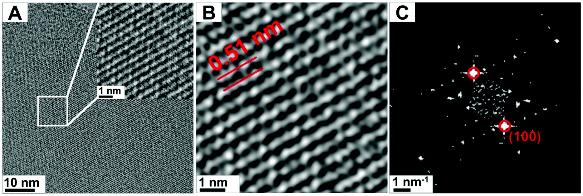 | ||
| Fig. 1 Low- and high-resolution TEM images of C3N4 nanosheets. (A) TEM crystalline image of the g-C3N4 lattice. The inset is of a cropped region showing the lattice in more detail. (B) Fourier filtered image of the inset presented in A. The lattice parameters were measured directly from the TEM image. (C) FFT of the image in B showing the lattice reflex attributed to the (100) plane. TEM images were acquired using an acceleration voltage of 300 kV and a current density of 4.0 × 10⁻¹¹ nA nm−2. | ||
Specimen stability studies at an acceleration voltage of 300 kV reveal that the g-C3N4 nanosheets were sensitive to electron irradiation. At low magnification (<165000×), it was possible to image the sample without visible changes to the flakes. This was achieved with a current density of up to 3.5 × 10⁻¹⁰ nA nm−2. However, when the magnification was increased to 210000×, the g-C3N4 nanosheets rapidly lost their crystalline structure during the same acquisition time (1 s). This happens because the current density is approximately two times larger (6.5 × 10⁻¹⁰ nA nm−2) for a magnification increase from 165000× to 210000×. Successful imaging of g-C3N4 with a magnification of 210000× was only possible by decreasing the current density to 4.0 × 10⁻¹¹ nA nm−2 (which was achieved by increasing the illumination area). At this low current density, the g-C3N4 lattice remained significantly more stable and could be irradiated for up to two minutes, which is sufficient for image capture with longer acquisition times. These results indicate that the current density is an important electron beam parameter concerning the stability of g-C3N4 nanosheets. Examples of the differences observed for different magnifications (and therefore current densities) are presented in Fig. 2A and B, which shows high-resolution TEM images of a g-C3N4 flake and its corresponding FFT, respectively. The image shown in Fig. 2A was acquired using a current density of 6.0 × 10⁻¹¹ nA nm−2. Suitable images with current densities up to 8.5 × 10⁻¹¹ nA nm−2 could be obtained, while for higher current densities, degradation was readily observed. An example of this degradation can be seen in Fig. 2D and E; panel D clearly shows the amorphous nature of the material after electron irradiation, as does the corresponding FFT in panel E, which lacks any reflexes and confirms the amorphous nature of the heavily irradiated samples. Typically, the transition to an amorphous state occurred after ∼20 s irradiation for current densities in the range of 4.0 × 10⁻¹⁰ to 6.0 × 10⁻¹⁰ nA nm−2 (one order of magnitude larger than that used in Fig. 2A). We also examined the stoichiometric changes between C and N in the material when transitioning from its crystalline state to an amorphous state through EELS probing studies. A representative example from a crystalline g-C3N4 state is shown in Fig. 2C, which displayed stoichiometric values of 62% C and 38% N. For the amorphous material obtained after extended electron irradiation, the stoichiometric values change to 96% C and 4% N (Fig. 2F). The EELS data, therefore, suggest a preferential loss of nitrogen from the g-C3N4 nanosheets during the transition process, ultimately yielding amorphous carbon.
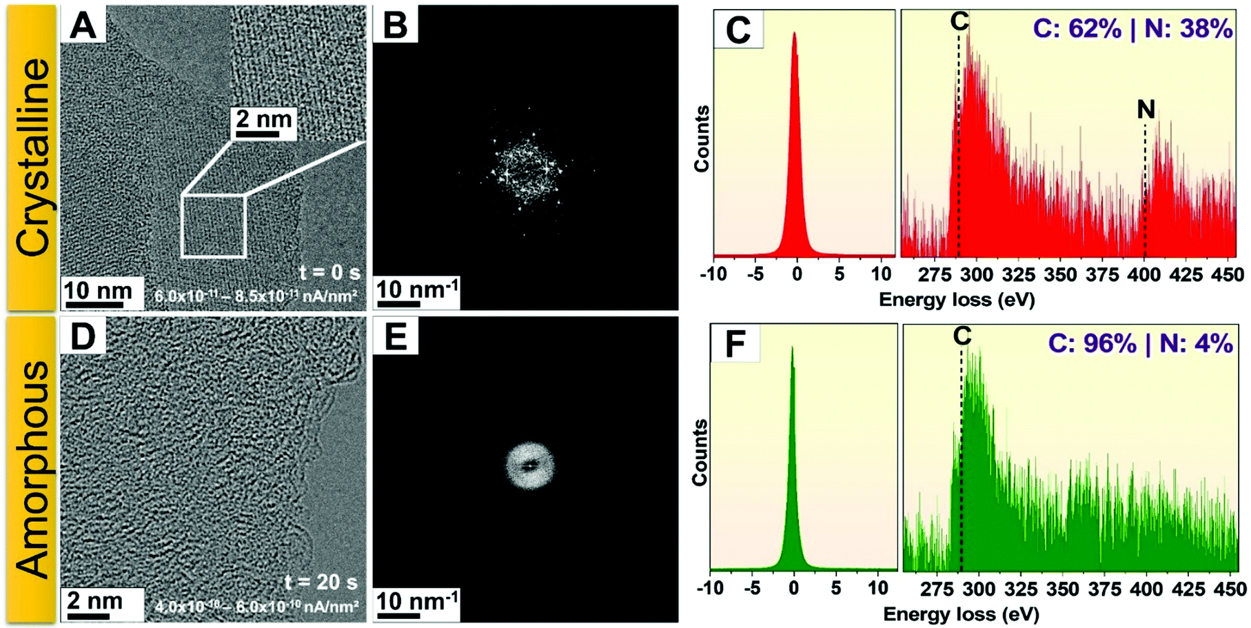 | ||
| Fig. 2 Sample of g-C3N4 sonicated for 180 s in isopropanol and imaged at 300 kV. (A) TEM image of the g-C3N4 nanosheet indicating that it is crystalline, as highlighted in the inset and in the FFT shown in panel (B). (C) EELS data showing the presence of carbon and nitrogen. (D) TEM image showing that after 20 s of electron irradiation, the g-C3N4 nanosheet quickly loses its crystallinity and becomes amorphous. (E) FFT showing the absence of reflexes in the amorphous state. (F) EELS data indicating that nitrogen is lost after electron irradiation. | ||
To further investigate the amorphization process and the stability of the g-C3N4 nanosheets, studies using an electron acceleration voltage of 80 kV were conducted. Reducing the acceleration voltage should, in principle, reduce the role of knock-on damage.25,28 The same experimental imaging conditions were used as were implemented at an electron acceleration voltage of 300 kV. Interestingly, the degradation of g-C3N4 was similar for both electron acceleration voltages (Fig. 3). Fig. 3A–C shows low magnification (31000×–99000×) TEM images for current densities in the range of 9.5 × 10⁻¹¹ to 3.5 × 10⁻¹⁰ nA nm−2, during which the g-C3N4 nanoflakes remained crystalline for up to 180 s. However, when the magnification was increased (165000–210000×), the total current density increased by one order of magnitude and the nanosheet transition to an amorphous state was again rapid and occurred within 20 s. EELS studies showed that this is related to the loss of nitrogen species in the material (for example shown in Fig. 1F).
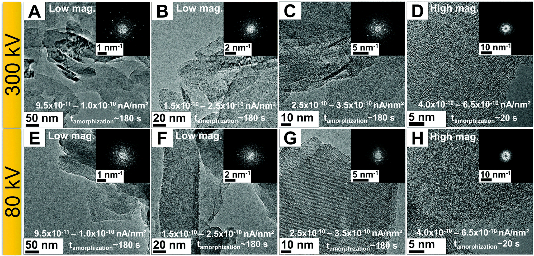 | ||
| Fig. 3 TEM images of g-C3N4 under different electron acceleration voltages. (A)–(D) TEM images of g-C3N4 at 300 kV. (A)–(C) Low magnification images show the presence of crystalline g-C3N4 nanosheets, as can be seen in the FFT insets. (D) Amorphization of the g-C3N4 nanosheet within 20 s after increasing current density. (E)–(H) TEM images of g-C3N4 imaged at 80 kV. (E)–(G) Low magnification images also show that the g-C3N4 nanosheets are crystalline. (H) Amorphous g-C3N4 after 20 s of electron irradiation at higher current density. | ||
To study the electron-beam-driven transition process, we also examined specimen stability at two lower acceleration voltages, namely, 60 and 30 kV. At lower acceleration voltages in the same current range explored at 80 and 300 kV (9.5 × 10⁻¹¹ to 6.0 × 10⁻¹⁰ nA nm−2), the crystalline g-C3N4 nanosheets became amorphous after exposure for 15 s with a current density of 6.0 × 10⁻¹⁰ nA nm−2. This suggests that the degradation of the g-C3N4 material occurs more readily at electron acceleration voltages below 80 kV.
To better comprehend the irradiation susceptibility of g-C3N4 at low electron acceleration voltages, a series of experiments using low current densities (1.0 × 10⁻¹¹ to 4.0 × 10⁻¹¹ nA nm−2) were conducted at acceleration voltages of 300, 80, 60, and 30 kV. At these lower current densities, successful image acquisition was only possible with longer exposure times (four times higher, 4 s). At low acceleration voltages, the image resolution decreased owing to increased electron scattering in the specimen and the predominance of lens aberrations.37 The resolution in TEM is limited by spherical (Cs) and chromatic (Cc) aberrations of the objective lenses.38 While the Cs occurs because electrons reach the optical axis at points slightly shifted from the image plane, Cc arises from energy spread in the electron beam, which causes electrons to focus at different image planes.38 At lower acceleration voltages, the Cc predominates. To overcome these image quality limitations at low acceleration voltages, it is essential to use a transmission electron microscope equipped with a Cc correction lens or an electron-beam monochromator.37,39,40 To obtain high-resolution images (Fig. 4), two imaging parameters (acceleration voltage and current density) were used. When a lower acceleration voltage was used, a lower current density was needed. Since electrons with low acceleration have a higher probability of interacting with the specimen (leading to an increase in electron-driven damage), one needs to reduce the current density to reduce the damage due to electron irradiation. However, this strategy can lead to poor image quality in addition to the lower resolution caused by the change in acceleration voltage. One can easily see that the image obtained at 300 kV (Fig. 4A) is of higher quality (is clearer) compared to that collected at 30 kV (Fig. 4D).
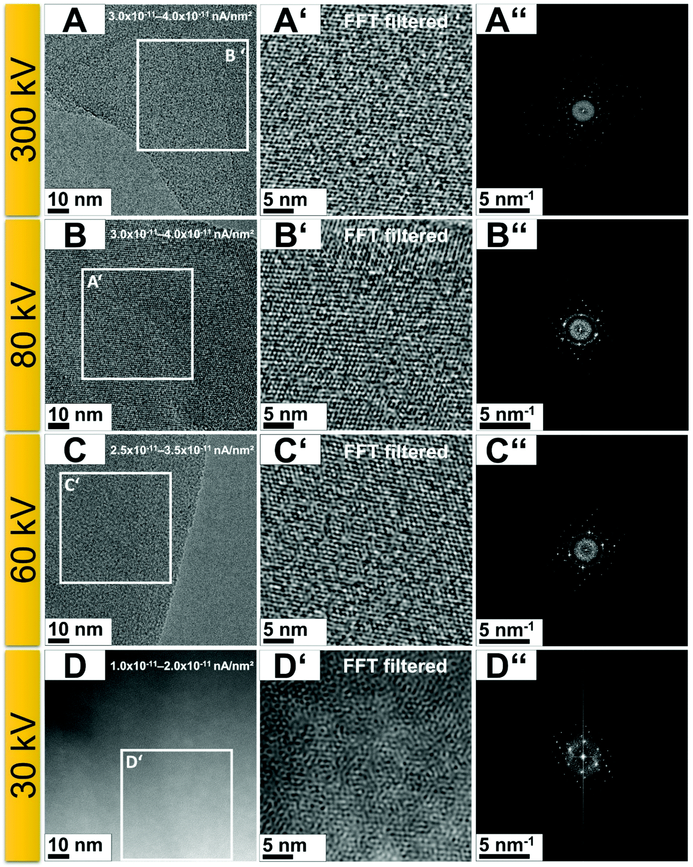 | ||
| Fig. 4 Differences in imaging C3N4 nanosheets with decreasing electron beam energy. TEM images of g-C3N4 at (A–A′′) 300 kV, (B–B′′) 80 kV, (C–C′′) 60 kV, and (D–D′′) 30 kV. (A′), (B′), (C′), and (D′) Fourier filtered images of the boxed regions in the TEM images, for 300, 80, 60, and 30 kV, respectively. The corresponding FFT images are shown in panels A′′, B′′, C′′ and D′′. In all cases, TEM imaging of g-C3N4 was performed using a low current density (1.0 × 10⁻¹¹ to 4.0 × 10⁻¹¹ nA nm−2). | ||
The microscopes used in this study are equipped with a Cs corrector at the objective lens as well as an electron monochromator. The electron monochromator reduces the electron energy spread and consequently reduces the Cc.37,38 Good-quality imaging at 60 kV (Fig. 4B) and 30 kV (Fig. 4D) was only possible by reducing the energy spread of the electron beam (also known as electron beam monochromation). With an electron acceleration voltage of 60 kV, it was possible to acquire images with reasonable image quality, whereas for an acceleration voltage of 30 kV, the image quality was visually limited, even when using a monochromated beam. Even with only a slight increase in current density (from 1.0 × 10⁻¹¹ to 4.0 × 10⁻¹¹ nA nm−2), the image quality deteriorates for the lowest acceleration voltages tested (60 and 30 kV) (Fig. S3, ESI†). For example, imaging with a current density of 6.0 × 10⁻¹¹ nA nm−2 (Fig. S3C and D, ESI†) led to image qualities significantly worse than when using a current density of 1.0 × 10⁻¹¹ nA nm−2 (Fig. S3C′ and D′, ESI†).
As mentioned in the introduction, there is an intrinsic correlation between the beam energy and the type of interaction with the specimen (either elastic or inelastic). Electron beams with high energies will favor elastic interactions (knock-on damage), whereas low-energy beams favor inelastic interactions (radiolysis). Therefore, the hypothesis to explain the observed phenomena is that with a decrease in the acceleration voltage, albeit with beam energy below the knock-on threshold energy, the energy transfer (inelastic interaction) from the incident beam to the specimen is high. At higher current densities, the greater the irradiation dose of the specimen, the more rapid the degradation of the lattice. As mentioned previously, this can produce defects on the g-C3N4 surface that are regions of instability in the lattice, which contribute to faster degradation of the material.
To better illustrate our observations, plots of the degradation time (amorphization time) for different electron acceleration voltages and currents are provided in Fig. 5. In Fig. 5A, amorphization of the g-C3N4 nanosheets is plotted against the acceleration voltage for two low current densities (on the order of 10−11 nA nm−2). It can be seen that for current densities between 1.0 × 10⁻¹¹ and 3.0 × 10⁻¹¹ nA nm−2, the nanosheets become amorphous over a time frame of approximately 120 s. With just a small increase in the current density (from 3.0 × 10⁻¹¹ to 4.0 × 10⁻¹¹ nA nm−2), the amorphization time decreases from 120 s to 30 s (reduction of 75%) for an acceleration voltage of 30 kV. Fig. 5B displays the amorphization time plotted as a function of the current density, which indicates that low-energy electron beams (30 and 60 kV) are more efficient at amorphizing the crystalline g-C3N4 nanosheets to amorphous carbon (due to the preferential release of N species). The preferential release of N can be thought of as akin to N defects in graphene. In graphene, the presence of dopants changes bond lengths as well as the local chemical properties, and are thus a source of instability that can facilitate degradation during electron irradiation.38 This is also observed with hexagonal boron nitride (h-BN), where B is preferentially removed over N from the graphene-like lattice.39–41
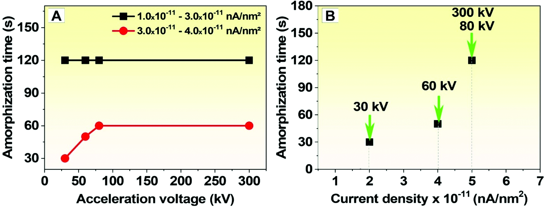 | ||
| Fig. 5 Comparison of the amorphization time, acceleration voltage, and current density. (A) Typical amorphization time plotted with respect to the microscope acceleration voltage for current densities above and below 3.0 × 10⁻¹¹ nA nm−2. (B) Typical amorphization time plotted according to microscope screen currents below 3.0 × 10⁻¹¹ nA nm−2, indicating that g-C3N4 is more stable at higher electron acceleration voltages. | ||
Moreover, since the C:N ratio (stoichiometry) may play an important role in the nature of the g-C3N4 lattice, and given that N appears to be ejected preferentially, we decided to investigate the loss of N in further detail. EELS data were collected for acceleration voltages of 300, 80, and 60 kV, as shown in Fig. 6A–C. Unfortunately, measurements for 30 kV were not possible owing to hardware limitations. The EELS spectra show that in all cases, the carbon peak (284 eV) and the nitrogen peak (401 eV) are present. However, the intensity of each peak varies for the different acceleration voltages used. Because the relative intensity of the EELS peaks is related to the elemental content in the specimen, the atomic content of carbon and nitrogen can be determined. Quantification of the EELS data suggests that the carbon content increases as the electron acceleration voltage decreases (Fig. 6D). The carbon and nitrogen content (given in molar %) measured at 300 kV was found to be 58% (±1%) and 42% (±1%), respectively. At 60 kV, the atomic content of the investigated elements was 79% (±1%) for carbon and 21% (±1%) for nitrogen.
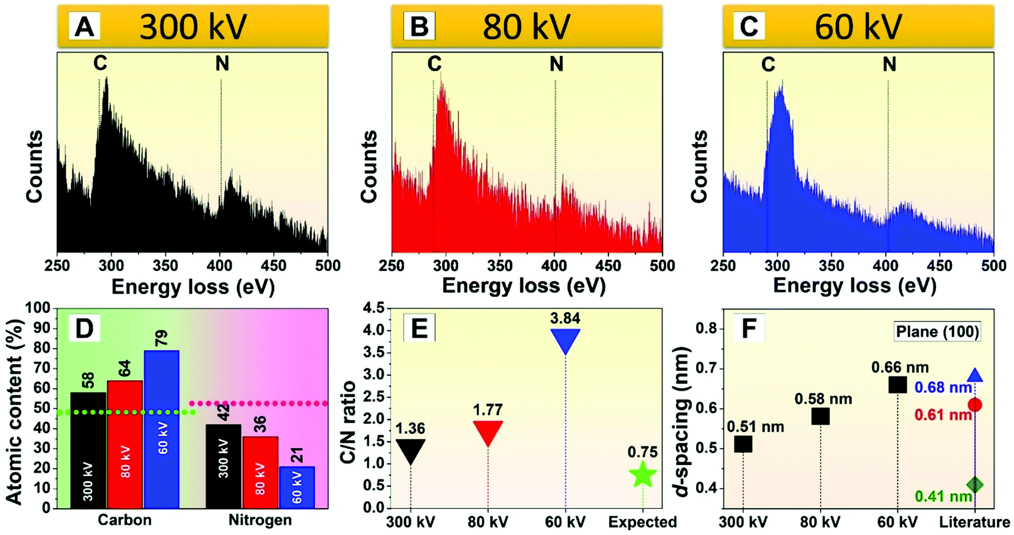 | ||
| Fig. 6 Chemical analysis of C3N4 nanosheets after irradiation with different electron beam energies. (A)–(C) EELS spectra of g-C3N4 measured using different acceleration voltages. Carbon and nitrogen were detected in all measurements. The atomic content for each measurement was quantified, with the relative amount of carbon increasing with decreasing acceleration voltage, whereas the opposite occurs for nitrogen, which decreases to a greater extent than carbon, as shown in panel (D). The theoretical atomic percentage for carbon and nitrogen for fully polymerized g-C3N4 are displayed as green and pink horizontal dotted lines, respectively. (E) The C:N ratio increases as the acceleration voltage decreases for 300, 80, and 60 kV. The green star indicates the C:N ratio described in the literature for fully polymerized g-C3N4. (F) The d-spacing of the (100) plane measured for 300, 80, and 60 kV compared to values published in the literature (see text). | ||
Since the interaction of the electron beam with the g-C3N4 nanosheets induces their transformation into amorphous carbon for all of the electron acceleration voltages tested – even with short exposure times – the accuracy of EELS quantification is therefore limited. This should be kept in mind when interpreting the data in comparison to the theoretical values of a completely non-irradiated flake. Since higher electron acceleration voltages interact less with the specimen, EELS data collected at 300 kV will be more accurate; however, in practice, we find that the values still differ from the theoretical values for fully polymerized g-C3N4 nanosheets (i.e., 48.48% for carbon, green dotted line; and 51.52% for nitrogen, pink dotted line in Fig. 6D. These values are relative to the atomic mass percentage).
Electron beam-induced stoichiometric changes are related to structural changes. As mentioned in the introduction, g-C3N4 can be obtained with various degrees of polymerization41–43 depending on the precursor materials and synthetic conditions, which play a crucial role in the polymerization of the final product and its subsequent properties.44 Our data show that under electron irradiation, there is a clear increase in the C:N ratio. The difference between the measured C:N34 changes significantly with the selected electron acceleration voltage, as shown in Fig. 6E. Our estimated C:N ratio when using 300, 80, and 60 kV acceleration voltages is much higher than the value reported for the ideal fully polymerized g-C3N4 (C:N ratio of 0.75), especially when the 60 kV electron beam was used. Because lower acceleration voltages increase the interaction cross-section of the electron beam with the specimen, the probability of radiolysis-induced damage increases.28,30,31 This confirms our observations that lower acceleration voltages remove nitrogen atoms more easily and faster (<20 s) from g-C3N4. However, it does not indicate which nitrogen atom is removed from g-C3N4 (C–N–C, NH or –NH2). This would require detailed mass spectroscopy analysis of C, H, and N before and after irradiation of a large amount of g-C3N4 (25–50 mg), which is not feasible in this instance.
Our data also show changes in the lattice d-spacings as N is preferentially removed from the g-C3N4 specimen under irradiation. The literature suggests that fully polymerized g-C3N4 exhibits smaller d-spacings when compared to partially polymerized materials. Our systematic data confirmed this trend. In our study, the d-spacing corresponding to the (100) plane measured with an acceleration voltage of 60 kV (0.66 nm) is larger than that at 80 kV (0.58 nm) and 300 kV (0.51 nm), as shown in Fig. 6F. It should be noted that there is a lack of clarity for the assignment of X-ray diffraction (XRD) based diffraction patterns for g-C3N4.45 For example, Wang et al.46 calculated the XRD results from the different phases of g-C3N4 and assigned the d-spacing for the (100) plane (space group P![[6 with combining macron]](https://www.rsc.org/images/entities/char_0036_0304.gif) m2) as 0.411 nm (Fig. 6F, green diamond). Tyborski et al.47 assigned the same (100) plane of a heptazine-based g-C3N4 (space group P3cm) with a d-spacing of 0.61 nm (Fig. 6F, red circle). Although both references point to the existence of different phases of g-C3N4, no investigation of the C:N ratio was considered. Experimental data by Fina et al.34 assigned the (100) peak to a d-spacing of 0.68 nm (Fig. 6F, blue triangle), which is larger than the calculated values mentioned above. They attributed the larger d-spacing to their sample being a partially polymerized g-C3N4 structure (C:N ratio of 0.68).
m2) as 0.411 nm (Fig. 6F, green diamond). Tyborski et al.47 assigned the same (100) plane of a heptazine-based g-C3N4 (space group P3cm) with a d-spacing of 0.61 nm (Fig. 6F, red circle). Although both references point to the existence of different phases of g-C3N4, no investigation of the C:N ratio was considered. Experimental data by Fina et al.34 assigned the (100) peak to a d-spacing of 0.68 nm (Fig. 6F, blue triangle), which is larger than the calculated values mentioned above. They attributed the larger d-spacing to their sample being a partially polymerized g-C3N4 structure (C:N ratio of 0.68).
Our results confirm that there is a correlation between the measured d-spacing and the C:N ratio. The electron beam produces structural damage in g-C3N4 across all examined acceleration voltages and current densities, changing the C:N ratio of g-C3N4 (degree of polymerization). This opens up new possibilities for tailoring the structure, and hence the properties, of g-C3N4 by selectively altering the d-spacing and C:N ratios with the use of electron beams. The ability to controllably engineer g-C3N4 to exhibit the desired function is attractive for specialized applications. For example, Gilbert et al.48 demonstrated the possibility of creating defined pore sizes in multilayer h-BN by controlling the vacancies introduced using an electron beam. They claim that such h-BN nanopores can be used for water desalination, molecular separation, and sensing. Similar possibilities can be expected with g-C3N4.
The enhancement of the catalytic properties of g-C3N4 has been demonstrated by introducing dopants,49 which is a strategy that can also improve its potential in sensor development.50 The synthesis of porous g-C3N4 using urea as a precursor showed promising results for the photocatalytic production of hydrogen by water splitting using sunlight.51 Tailoring the nitrogen content of g-C3N4 also opens up the possibility of improving energy storage technologies.52 Chen et al.53 demonstrated that nitrogen-deficient g-C3N4 exhibits high electrochemical performance for lithium-ion battery applications. The increase in d-spacing due to changes in the C:N ratio of g-C3N4 as the result of bond breakage also creates new active sites, which could, for example, enhance the photocatalytic properties of g-C3N4. We also envision the possibility of incorporating tailored g-C3N4 in devices to detect radiation doses, for diverse applications in space exploration, biomedical radiation treatment, or nuclear power plants.
Conclusions
The work at hand presents an approach to selective change the stoichiometry of g-C3N4 nanosheets using an electron beam with different energies and current densities. In this way, our approach provides a facile method to control the C:N ratio of g-C3N4 and, as a result, the physical properties of the material. The g-C3N4 nanosheets degrade over time under electron irradiation for all explored electron acceleration voltages and current densities. Systematic EELS studies indicate that N was preferentially lost, such that amorphous carbon eventually remained. Through the careful temporal tracking of the process, the structural changes in-between crystalline and amorphous phases revealed that as N is lost, the lattice d-spacing increases. Corresponding EELS studies allowed us to correlate the d-spacing changes with the stoichiometry of the g-C3N4. The material with stoichiometry could be altered by changing both the electron acceleration voltage and current density. Faster deterioration was clearly observed for the lower acceleration voltages studied (≤60 kV), suggesting that inelastic scattering (radiolysis) is the predominant material loss mechanism. The rate of change (material loss) also increased with increasing current density, increasing rapidly above a certain threshold. These findings indicate that with a careful adjustment of the electron acceleration voltage or current density, the nitrogen content of the crystalline g-C3N4 nanosheets can be modified. This work not only provides fundamental insight into the stability of g-C3N4 under electron irradiation, but also allows the tailoring of the stoichiometry of g-C3N4, and thus broadens its potential for applications such as photocatalysis, energy storage, and sensing.
Author contributions
The experiment was devised and managed by MHR. RGM conducted the TEM experiments and primary data analysis. AM and BBI prepared the g-C3N4 material. RGM, HQT, XY, AB, PP, AM, BBI, RS, TG and MHR contributed to the data analysis and preparation as well manuscript preparation.Conflicts of interest
There are no conflicts to declare.Acknowledgements
This work was supported by the National Natural Science Foundation of China (Grant No. 52071225) and the Czech Republic from ERDF “Institute of Environmental Technology – Excellent Research” (No. CZ.02.1.01/0.0/0.0/16_019/0000853). MHR thanks the Sino-German Research Institute for support (project: GZ 1400). XQY thanks Suzhou University. HQT thanks the Alexander Von Humboldt Foundation for support through a fellowship. PP acknowledges the Czech Science Foundation (Project No. 19-15199 S).References
- X. Wang, S. Blechert and M. Antonietti, ACS Catal., 2012, 2, 1596–1606 CrossRef CAS.
- J. Wen, J. Xie, X. Chen and X. Li, Appl. Surf. Sci., 2017, 391, 72–123 CrossRef CAS.
- A. Wang, C. Wang, L. Fu, W. Wong-Ng and Y. Lan, Nano-Micro Lett., 2017, 9, 1–21 CrossRef.
- N. Rono, J. K. Kibet, B. S. Martincigh and V. O. Nyamori, Crit. Rev. Solid State, 2020, 1–29 Search PubMed.
- K. Wang, D. Shao, L. Zhang, Y. Zhou, H. Wang and W. Wang, J. Mater. Chem. A, 2019, 7, 20383–20389 RSC.
- J. Safaei, N. A. Mohamed, M. F. Mohamad Noh, M. F. Soh, N. A. Ludin, M. A. Ibrahim, W. N. Roslam Wan Isahak and M. A. Mat Teridi, J. Mater. Chem. A, 2018, 6, 22346–22380 RSC.
- M. Ismael and Y. Wu, Sustainable Energy Fuels, 2019, 3, 2907–2925 RSC.
- M. Xiong, Q. Rong, H. Meng and X. Zhang, Biosens. Bioelectron., 2017, 89, 212–223 CrossRef CAS.
- G. Liao, F. He, Q. Li, L. Zhong, R. Zhao, H. Che, H. Gao and B. Fang, Prog. Mater. Sci., 2020, 112, 100666 CrossRef CAS.
- H. Zhao, M. Lei, X. Yang, J. Jian and X. Chen, J. Am. Chem. Soc., 2005, 127, 15722–15723 CrossRef CAS.
- P. G. Li, M. Lei, Z. B. Sun, L. Z. Cao, Y. F. Guo, X. Guo and W. H. Tang, J. Alloys Compd., 2007, 430, 237–240 CrossRef CAS.
- A. Thomas, A. Fischer, F. Goettmann, M. Antonietti, J. O. Müller, R. Schlögl and J. M. Carlsson, J. Mater. Chem., 2008, 18, 4893–4908 RSC.
- N. Cheng, P. Jiang, Q. Liu, J. Tian, A. M. Asiri and X. Sun, Analyst, 2014, 139, 5065–5068 RSC.
- X. Cao, J. Ma, Y. Lin, B. Yao, F. Li, W. Weng and X. Lin, Spectrochim. Acta, Part A, 2015, 151, 875–880 CrossRef CAS.
- Y. C. Lu, J. Chen, A. J. Wang, N. Bao, J. J. Feng, W. Wang and L. Shao, J. Mater. Chem. C, 2015, 3, 73–78 RSC.
- L. Feng, F. He, G. Yang, S. Gai, Y. Dai, C. Li and P. Yang, J. Mater. Chem. B, 2016, 4, 8000–8008 RSC.
- G. Liao, Y. Gong, L. Zhang, H. Gao, G. J. Yang and B. Fang, Energy Environ. Sci., 2019, 12, 2080–2147 RSC.
- J. Barrio, M. Volokh and M. Shalom, J. Mater. Chem. A, 2020, 8, 11075–11116 RSC.
- H. Liu, X. Wang, H. Wang and R. Nie, J. Mater. Chem. B, 2019, 7, 5432–5448 RSC.
- Q. Hao, G. Jia, W. Wie, A. Vinu, Y. Wang, H. Arandiyan and B.-J. Ni, Nano Res., 2020, 13, 18–37 CrossRef CAS.
- S. Patnaik, S. Martha and K. M. Parida, RSC Adv., 2016, 6, 46929–46951 RSC.
- X. Wang, K. Maeda, A. Thomas, K. Takanabe, G. Xin, J. M. Carlsson, K. Domen and M. Antonietti, Nat. Mater., 2009, 8, 76–80 CrossRef CAS.
- R. C. Pawar, S. Kang, J. H. Park, J. H. Kim, S. Ahn and C. S. Lee, Sci. Rep., 2016, 6, 1–14 CrossRef.
- R. F. Egerton, Electron Energy-Loss Spectroscopy in the Electron Microscope, 3rd edn, Springer-Verlag, New York, 2014 Search PubMed.
- M. H. Rümmeli, H. Q. Ta, R. G. Mendes, I. G. Gonzalez-Martinez, L. Zhao, J. Gao, L. Fu, T. Gemming, A. Bachmatiuk and Z. Liu, Adv. Mater., 2019, 31, 1800715 CrossRef.
- R. G. Mendes, J. Pang, A. Bachmatiuk, H. Q. Ta, L. Zhao, T. Gemming, L. Fu, Z. Liu and M. H. Rümmeli, ACS Nano, 2019, 13, 978–995 CAS.
- J. Cazaux, Ultramicroscopy, 1995, 60, 411–425 CrossRef CAS.
- J. Tao, R. Wang and H. Zhang, Progress in Nanoscale Characterization and Manipulation, Springer, Beijing, 2018, pp. 1–34 Search PubMed.
- J. C. Meyer, F. Eder, S. Kurasch, V. Skakalova, J. Kotakoski, H. J. Park, S. Roth, A. Chuvilin, S. Eyhusen, G. Benner, A. V. Krasheninnikov and U. Kaiser, Phys. Rev. Lett., 2012, 108, 239902 Search PubMed.
- R. F. Egerton, Micron, 2019, 119, 72–87 CrossRef CAS.
- R. F. Egerton, Microsc. Res. Tech., 2012, 75, 1550–1556 CrossRef CAS.
- Y. Dai, Q. Bu, R. Sooriyagoda, P. Tavadze, O. Pavlic, T. Lim, Y. Shen, A. Mamakhel, X. Wang, Y. Li, H. Niemantsverdriet, B. B. Iversen, F. Besenbacher, T. Xie, J. P. Lewis, A. D. Bristow, N. Lock and R. Su, J. Phys. Chem. Lett., 2019, 10, 5381–5386 CrossRef CAS.
- Y. Kang, Y. Yang, L. C. Yin, X. Kang, G. Liu and H. M. Cheng, Adv. Mater., 2015, 27, 4572–4577 CrossRef CAS.
- F. Fina, S. K. Callear, G. M. Carins and J. T. S. Irvine, Chem. Mater., 2015, 27, 2612–2618 CrossRef CAS.
- D. M. Teter and R. J. Hemley, Science, 1996, 271, 53–55 CrossRef CAS.
- S. C. Yan, Z. S. Li and Z. G. Zou, Langmuir, 2009, 25, 10397–10401 CrossRef CAS.
- R. F. Egerton, Ultramicroscopy, 2014, 145, 85–93 CrossRef CAS.
- P. C. Tiemeijer, M. Bischoff, B. Freitag and C. Kisielowski, Ultramicroscopy, 2012, 114, 72–81 CrossRef CAS.
- U. Kaiser, J. Biskupek, J. C. Meyer, J. Leschner, L. Lechner, H. Rose, M. Stöger-Pollach, A. N. Khlobystov, P. Hartel, H. Müller, M. Haider, S. Eyhusen and G. Benner, Ultramicroscopy, 2011, 111, 1239–1246 CrossRef CAS.
- D. C. Bell, C. J. Russo and D. V. Kolmykov, Ultramicroscopy, 2012, 114, 31–37 CrossRef CAS.
- J. Wu, X. Ji, X. Yuan, Z. Zhao, Y. Li, B. Wen, H. Zhang, D. Yu, Y. Zhao and Y. Tian, Chem. Mater., 2019, 31, 9188–9199 CrossRef CAS.
- A. Zambon, J. M. Mouesca, C. Gheorghiu, P. A. Bayle, J. Pécaut, M. Claeys-Bruno, S. Gambarelli and L. Dubois, Chem. Sci., 2016, 7, 945–950 RSC.
- V. W. H. Lau, M. B. Mesch, V. Duppel, V. Blum, J. Senker and B. V. Lotsch, J. Am. Chem. Soc., 2015, 137, 1064–1072 CrossRef CAS.
- J. Wu, X. Ji, X. Yuan, Z. Zhao, Y. Li, B. Wen, H. Zhang, D. Yu, Y. Zhao and Y. Tian, Chem. Mater., 2019, 31, 9188–9199 CrossRef CAS.
- B. W. Sun, H. Y. Yu, Y. J. Yang, H. J. Li, C. Y. Zhai, D. J. Qian and M. Chen, Phys. Chem., 2017, 19, 26072–26084 CAS.
- J. Wang, J. Lei and R. Wang, Phys. Rev. B: Condens. Matter Mater. Phys., 1998, 58, 11890 CrossRef CAS.
- T. Tyborski, C. Merschjann, S. Orthmann, F. Yang, M. C. Lux-Steiner and T. Schedel-Niedrig, J. Phys.: Condens. Matter, 2013, 25, 395402 CrossRef CAS.
- S. M. Gilbert, G. Dunn, A. Azizi, T. Pham, B. Shevitski, E. Dimitrov, S. Liu, S. Aloni and A. Zettl, Sci. Rep., 2017, 7, 1–7 CrossRef CAS.
- Z. Pei, J. Gu, Y. Wang, Z. Tang, Z. Liu, Y. Huang, Y. Huang, J. Zhao, Z. Chen and C. Zhi, ACS Nano, 2017, 11, 6004–6014 CrossRef CAS.
- M. M. Xavier, P. R. Nair and S. Mathew, Analyst, 2019, 144, 1475–1491 RSC.
- Y. Zhang, J. Liu, G. Wu and W. Chen, Nanoscale, 2012, 4, 5300–5303 RSC.
- J. Liu, Y. Zhang, L. Zhang, F. Xie, A. Vasileff and S. Z. Qiao, Adv. Mater., 2019, 31, 1901261 CrossRef.
- J. Chen, Z. Mao, L. Zhang, D. Wang, R. Xu, L. Bie and B. D. Fahlman, ACS Nano, 2017, 11, 12650–12657 CrossRef CAS.
Footnote |
| † Electronic supplementary information (ESI) available: Supplementary material with further description of the experimental steps and influence of time and current density. See DOI: 10.1039/d0cp06518h |
| This journal is © the Owner Societies 2021 |