New theoretical insights into the photoinduced carrier transfer dynamics in WS2/WSe2 van der Waals heterostructures†
Received
26th August 2020
, Accepted 6th November 2020
First published on 9th November 2020
Abstract
Shedding light on the dynamics of charge transfer is fundamental and important to understand the light-photocurrent power conversion in transition-metal dichalcogenide (TMD) heterostructures. Herein, based on time-dependent ab initio nonadiabatic molecular dynamics simulation, we studied the photoinduced carrier transfer dynamics in the WS2/WSe2 heterostructure and further analyzed the effects of stacking configuration and temperature. Our calculations show that the time scales of ultrafast hole transfer in the C7 and T stacking configurations are 35 fs and 30 fs, respectively, which are mainly caused by the adiabatic charge transfer mechanism. Meanwhile, the time scales of ultrafast electron transfer in the C7 and T stacking configurations are 12 fs and 40 fs, respectively, which are in good agreement with the experimental result. We also investigated in detail the photoinduced carrier transfer pathways of C7 and T stacking configurations, which appear to have some significant differences. In addition, we found that the temperature basically has no effect on the electron transfer dynamics of the WS2/WSe2 heterostructure; this is in excellent agreement with the experimental observation. In short, the reported findings can provide more in-depth insights into the photoinduced carrier transfer dynamics of TMD-based van der Waals heterostructures.
1. Introduction
Recently, van der Waals (vdW) heterostructures composed of two-dimensional (2D) transition metal dichalcogenides (TMD) have attracted extensive attention due to their unique optical and electronic properties, and thus have a great application prospect in the field of advanced 2D photo/electrocatalytic devices.1–6 Up to now, extensive efforts on TMD vdW heterostructures have been reported experimentally and theoretically. Remarkably, the photoinduced carrier transfer in the TMD heterostructures as a fundamental photophysical process plays an extremely crucial role in 2D optoelectronic devices, photovoltaic materials and photocatalysis.7–12
Interestingly, it has been reported that most of the TMD heterostructures, including MoS2/WS2, MoSe2/WSe2, MoS2/WSe2, MoS2/MoSe2, etc., are predicted to form typical type-II heterostructures, which are theoretically beneficial to the effective separation of photoexcited electrons and holes.13–21 As early as in 2014, Hong et al. firstly experimentally reported that the photoexcited hole transfer from the MoS2 layer to the WS2 layer takes place within 50 fs.7 Since then, the charge transfer in TMD heterostructures has gradually become one of the most attractive hotspots. For instance, Peng et al. observed that the photoexcited electron transfer from the MoS2 layer to the WSe2 layer occurs within 470 fs.9 Zhou et al. confirmed that the electron transfer at a WS2/WSe2 heterostructure is ultrafast (∼30 fs).22 On the theoretical aspect, Long et al. utilized time-domain density functional theory combined with nonadiabatic molecular dynamics to investigate the photoinduced charge separation and recombination dynamics at a MoS2/MoSe2 heterostructure and revealed that the interfacial quantum coherence promotes the efficient charge separation.23 Time-dependent density functional theory molecular dynamics was adopted by Wang et al. to study the charge transfer across the interface of the MoS2/WS2 heterostructure.24 They presented that the collective motion leads to the dramatic non-linear charge oscillations. Ji et al. uncovered that the charge transfer at a MoS2/WS2 heterostructure is robust against varying interlayer twist angles and interlayer coupling strength, in the time scale of ∼90 fs.25 In addition, Zhang et al. reported the discovery of an interfacial pathway at a MoS2/WSe2 heterostructure for the relaxation of photoexcited hot electrons through interlayer hopping, which is significantly faster than intralayer relaxation.19 Effective carrier separation is a key factor to realize the photon–electron and solar energy conversion in the photoelectric devices, and this process is mainly accomplished by ultrafast charge transfer, with the time scale ranging from tens to hundreds of femtoseconds. Even though some progress has been made in the work of the charge transfer dynamics in TMD heterostructures, it is still in the preliminary stage and there remains a lack of comprehensive and in-depth understanding. And it is urgent and rather meaningful to theoretically further explore the charge transfer in TMD heterostructures.
Motivated by this, the goal of this work is to theoretically provide much useful information about the photoinduced carrier transfer process in the WS2/WSe2 vdW heterostructure based on time-dependent ab initio nonadiabatic molecular dynamics simulation (NAMD). In the present work, we investigated both the hole and electron transfer processes, whose schematic diagrams are plotted in Fig. 3a. Furthermore, the effects of the stacking configuration and temperature on the photoinduced carrier dynamics of the system are considered in the present article, which can promote a deeper understanding of the photoinduced carrier dynamics in TMD heterostructures. A detailed analysis of simulated results agrees well with the experimental data, providing important insights for the future functional design of TMD-based van der Waals heterostructures.
2. Computational details
Density functional theory calculations are implemented in the Vienna ab initio simulation package (VASP).26,27 The projector augmented wave (PAW) method is employed to describe the electron–nucleus interaction.28 The electron exchange and correlation functionals were treated by the Perdew–Burke–Ernzerhof (PBE) functional of the generalized gradient approximation (GGA).29 The energy cutoff for the plane-wave expansion is set to 500 eV. All the systems are fully relaxed until the total energy and atomic forces are smaller than 10−5 eV and 0.001 eV Å−1, respectively. The DFT-D2 method is used to describe the vdW interaction.30 In order to avoid interaction between two adjacent periodic images, a 20 Å vacuum region was adopted in this study.
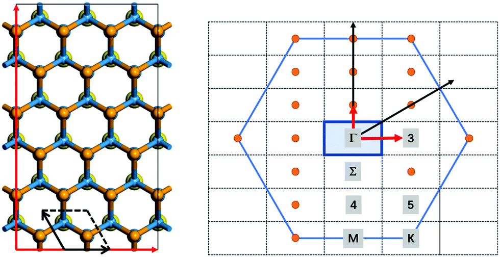
All ab initio NAMD simulations are performed using the Hefei-NAMD code within the theoretical framework of time-dependent density functional theory (TDDFT) and fewest-switch surface hopping (FSSH), which has been successfully and widely applied in several studies of the photoexcited carrier transfer dynamics in semiconducting materials.18,31–36 In this work, an orthogonal 3 × 3 supercell with 108 atoms of the WS2/WSe2 heterostructure is built to simulate the dynamic process at the Γ-point, as shown in Fig. 1. Firstly, the geometric and electronic structures are optimized at 0 K. Then, the velocity rescaling method is used to bring the temperature of the considered system to either 78 K or 300 K.36 A 5 ps microcanonical ab initio molecular dynamics trajectory is then generated with a time step of 1 fs. Using the molecular dynamics trajectory, the simulated NAMD results are based on averaging over 100 different initial configurations. For each chosen structure, 2 × 10⁴ trajectories for the last 2 ps are sampled. More calculation details can be found in the ESI.†
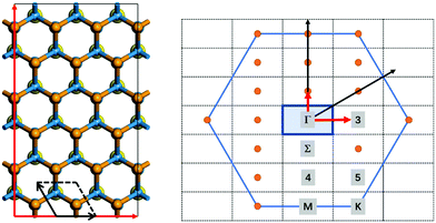 |
| | Fig. 1 The primitive cell and supercell of the WS2/WSe2 heterostructure (left) and the corresponding high symmetric K-points (right). | |
3. Results and discussion
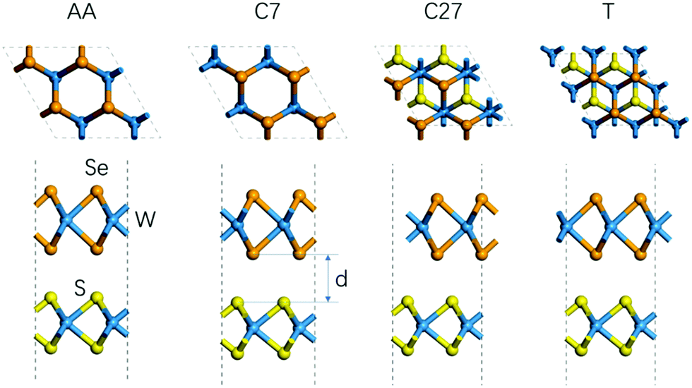
First, we studied the geometric and band structures of pristine WS2 and WSe2 monolayers. The relaxed lattice constants are 3.19 Å and 3.30 Å, respectively, for an isolated unit cell of WS2 and WSe2 monolayers, and the corresponding band gaps are 1.82 eV and 1.59 eV, which are consistent with the reported theoretical values.37–39 In order to reduce the unnecessary strain effect, the WS2/WSe2 heterostructure has a hexagonal lattice with a = 3.25 Å, with the lattice mismatch ≤2%. According to the theoretical reference, we model four different stacking configurations, as shown in Fig. 2.17Table 1 lists the total energy and layer distance of the WS2/WSe2 heterostructure for four different stacking configurations. We found that the C7 stacking configuration is the most stable due to its lowest total energy, which is in line with the experimental results reported previously.40 Moreover, the T stacking configuration, referred to as another experimentally stable structure, was also chosen to study the effect of the stacking configuration. Then, we calculated and analyzed the band structures of C7 and T stacking configurations, as plotted in Fig. 3b and c. It demonstrated that C7 and T stacking configurations both have a type-II band alignment, whose direct band gaps are 0.82 eV and 0.75 eV, respectively. In addition, for the C7 and T stacking configurations, the valence band maxima (VBM) both are mainly contributed by the d orbital of the W atom and the p orbital of the Se atom in the WSe2 layer, while the conduction band minima (CBM) are mainly contributed by the d orbital of the W atom in the WS2 layer.
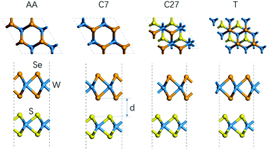 |
| | Fig. 2 Side view and top view of the WS2/WSe2 heterostructure of different stackings (i.e., C7, C27, AA, and T). | |
Table 1 The total energy and layer distance of the WS2/WSe2 heterostructure for four different stacking configurations. The total energy of the C7 stacking configuration was selected as a reference point
| Stacking configurations |
AA |
C7 |
C27 |
T |
| Total energy (eV) |
0.181 |
0.000 |
0.022 |
0.010 |
| Layer distance (Å) |
3.211 |
3.088 |
3.100 |
3.092 |
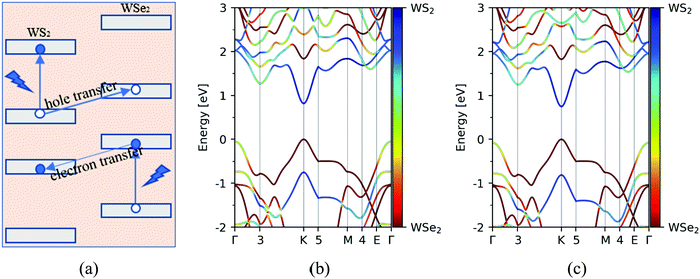 |
| | Fig. 3 (a) Schematic diagrams of the photoinduced hole and electron transfer processes at the WS2/WSe2 heterostructure. Band structures of WS2/WSe2 heterostructures with C7 (b) and T (c) stacking configurations. | |
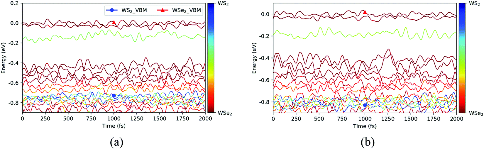
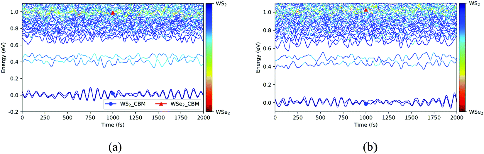
Before exploring the photoinduced hole transfer dynamics, we analyzed in detail the time evolutions of the energy states near the VBM for the C7 and T stacking configurations at 300 K, as displayed in Fig. 4. As seen from Fig. 4a for the C7 stacking configuration, the VBM (WSe2@K) energy states, represented by two red lines, oscillate in the vicinity of 0 eV during the MD trajectory. In the range of [−0.2, −0.1] eV, the one light-green line represents the VB energy state at the Γ point on WS2 (WS2@Γ), in which occurred strong orbital hybridization. In the range of [−0.6, −0.4] eV, there are four red lines representing the VB energy states at the 5 point on WSe2 (WSe2@5). In the range of [−0.7, −0.6] eV, the two light-red lines represent the VB energy states at the Σ point on WSe2(WSe2@Σ). In the energy range of [−0.8, −0.7] eV, there exist six strongly hybridized energy state lines, and the VBM energy states (WSe2@K) of the WS2 layer are mainly located in this energy range, which is set to the initial states of the NAMD simulations. Similarly, the time evolutions of the energy states near the VBM do not show significant difference except the larger oscillation amplitude for the T stacking configuration, as shown in Fig. 4b. This can be caused by different electron–phonon couplings and initial phonon excitation.36
 |
| | Fig. 4 Time evolutions of the energy states near the VBM for the C7 (a) and T (b) stacking configurations at 300 K. | |
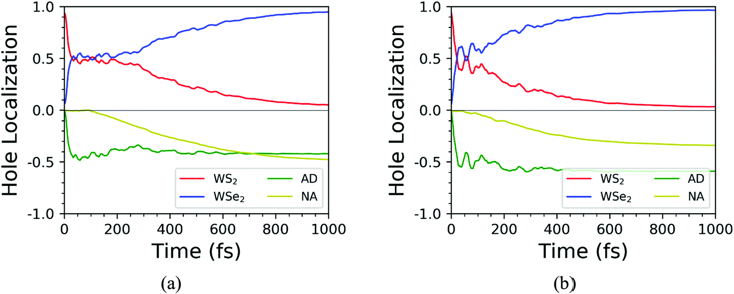
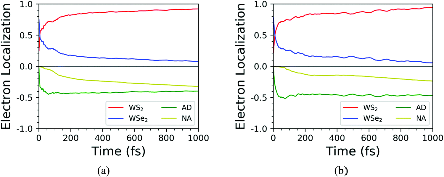
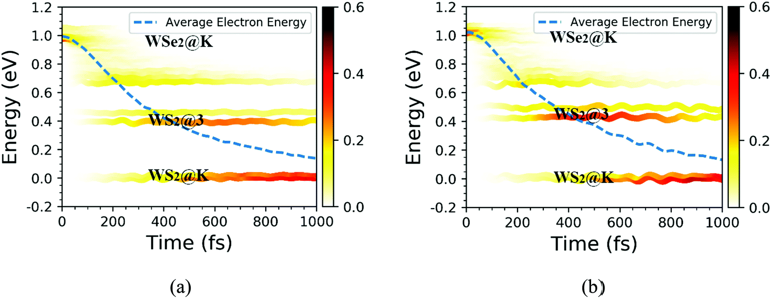
Based on the NAMD calculations, we obtained the time-dependent spatial hole localization for the C7 and T stacking configurations at 300 K, as shown in Fig. 5. Moreover, by assessing the hole probability distribution for selected energy states, we deduced the time-dependent hole-energy change, as indicated in Fig. 6. Interestingly, the relaxation dynamics of photoinduced hole transfer can be divided into three stages for the C7 and T stacking configurations. For the C7 stacking configuration from Fig. 5a, the ultrafast stage corresponds to a hole transfer from the WS2 layer to the WSe2 layer within τ1 ≈ 35 fs, whereby the hole distribution on the WSe2 layer increases from 6% to 52%. Then, the platform stage involves an intralayer hole relaxation with the τ2 ≈ 155 fs time scale, whereby the hole distribution on WSe2 almost never changes. The slow stage involves a hole relaxation with the τ3 ≈ 382 fs time scale, whereby the hole distribution on the WSe2 layer slowly increases and converges to 95%. In addition, the transfer pathway of photoinduced holes in the WS2 layer is discussed as plotted in Fig. 6a. This transfer pathway is WS2@K → WSe2@5 → WSe2@K, which is also accompanied by slowly diverging hole transfer.
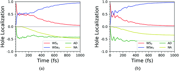 |
| | Fig. 5 Time-dependent spatial hole localization for the C7 (a) and T (b) stacking configurations at 300 K. | |
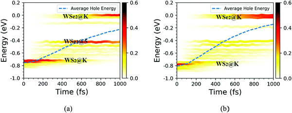 |
| | Fig. 6 Time-dependent hole energy change for the C7 and T stacking configurations at 300 K. The color strips and dashed lines indicate the hole distribution on different energy states and the averaged hole energy, respectively. | |
As a comparison, we study the photoinduced hole transfer dynamics in the T stacking configuration at 300 K. The hole transfer is also divided into three stages, as shown in Fig. 5b. The first stage is an ultrafast hole transfer process with the time scale of 30 fs, in which the hole spatial distribution of the WSe2 layer increased from 6% to 60%. The second stage is a platform process, in which the hole transfer occurs within the WS2 layer because the hole spatial distribution in each layer is almost unchanged, with a time scale of 95 fs. The third stage is a slow hole transfer process. The hole spatial distribution of the WSe2 layer slowly increases to 96%, and the time scale is 241 fs. As seen from Fig. 6b, the photoinduced hole transfer path of the WS2 layer is mainly WS2@K → WSe2@K. In addition, the average energy evolutions of the photoexcited hole for the C7 and T stacking configurations are also analyzed. By means of exponential decay fitting, the time scales of C7 and T stacking configurations are 2.36 ns and 1.23 ns, respectively, which are far behind the change of the hole spatial distribution, further indicating that the time for simulating photoexcited hole transfer dynamics of the WS2/WSe2 heterostructure within 1 ps is sufficient.41
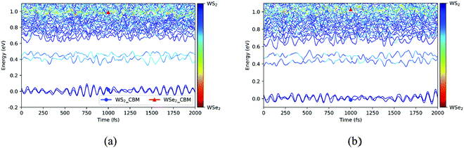
Next, we explored the photoexcited electron transfer for the C7 and T stacking configurations at 300 K. The time evolutions of the energy states near the CBM for the C7 and T stacking configurations at 300 K was analyzed, as shown in Fig. 7. As mentioned previously, the ground state molecular dynamics results of C7 and T stacking configurations are relatively consistent. For the C7 stacking configuration, as seen from Fig. 7a, there are two blue lines near 0 eV, which correspond to WS2@K. In the range of 0.4–0.5 eV, there are two light-blue lines corresponding to WSe2@3. In addition, there are strong orbital hybridization and energy level crossing around 1.0 eV, which correspond to the CBM energy states of the WSe2 layer, namely WSe2@K.
 |
| | Fig. 7 Time evolutions of the energy states near the CBM for the C7 (a) and T (b) stacking configurations at 300 K. | |
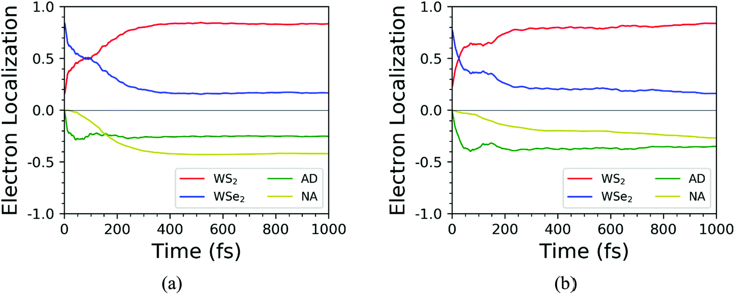
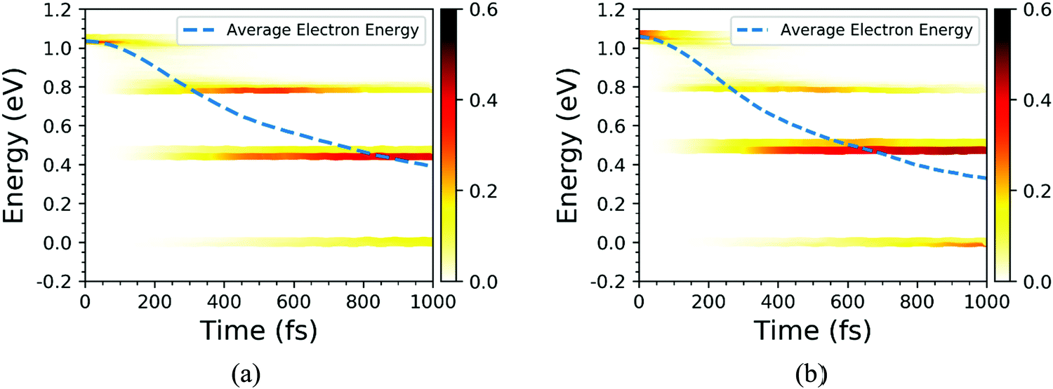
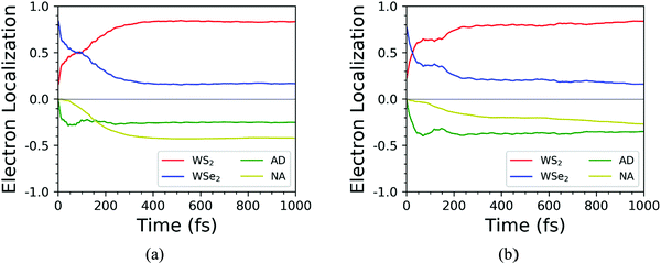
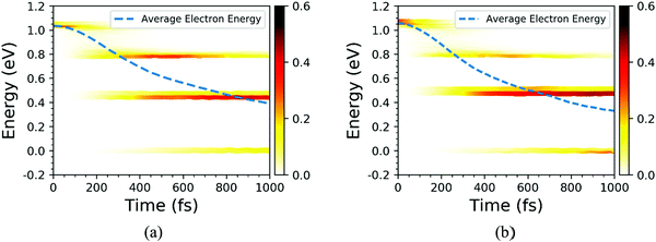
We further discussed the time-dependent spatial electron localization for the C7 and T stacking configurations at 300 K, as plotted in Fig. 8. For the C7 stacking configuration, it can be seen from Fig. 8a that the photoexcited electron transfer dynamics is mainly divided into two stages. The first stage is an ultrafast electron transfer process with a time scale of about 12 fs, which is in great agreement with the experimental observation.22 The spatial electron distribution in the WS2 layer increases from 24% to 57%, which is mainly caused by the adiabatic charge transfer mechanism. The second stage is a slowly photoexcited electron transfer process with a time scale of electron transfer of 156 fs, which is mainly caused by the non-adiabatic charge transfer mechanism. In the meantime, the spatial electron distribution in the WS2 layer increases and converges at 92%. Fig. 9 shows the time-dependent electron energy change for the C7 and T stacking configurations at 300 K. Therefore, as seen from Fig. 9a, the transfer pathway of photoexcited electrons for the C7 stacking configuration is analyzed, that is, WSe2@K → WS2@3 → WS2@K.
 |
| | Fig. 8 Time-dependent spatial electron localization for C7 (a) and T (b) stacking configurations at 300 K. | |
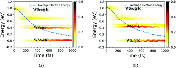 |
| | Fig. 9 Time-dependent electron energy change for the C7 and T stacking configurations at 300 K. The color strips and dashed lines indicate the electron distribution on different energy states and the averaged electron energy, respectively. | |
Likewise, the time-dependent spatial hole localization for the T stacking configuration at 300 K was analyzed, as plotted in Fig. 8b. We noted that the photoexcited electron transfer dynamics can also be divided into two stages. The first stage is an ultrafast electron transfer process with a time scale of 40 fs, which is consistent with the experimental observation results.22 The spatial electron distribution in the WS2 layer increases from 22% to about 70%, which is mainly caused by the adiabatic charge transfer mechanism. The second stage is a slow electron transfer process with a time scale of 483 fs, which is mainly caused by the non-adiabatic charge transfer mechanism. The spatial electron distribution in the WS2 layer has been slowly increasing and finally balanced at 94%. As can be seen from Fig. 9b, the transfer pathway of photoexcited electrons for the T stacking configuration is WSe2@K → WS2@3 → WS2@K, which is the same as that of the C7 stacking configuration. In addition, we also obtained the time scales of the electron average energy for the C7 and T stacking configurations, suggesting that the NAMD simulations within 1 ps are enough to study the photoexcited electron transfer dynamics processes.
Finally, the influence of temperature on the photoexcited electron transfer dynamics of C7 and T stacking configurations was studied, and thus the NAMD results of 78 K were selected as a comparison. As seen from Fig. S1 (ESI†), compared with the NAMD results at 300 K, the oscillation amplitude of the energy states near the CBM for the C7 and T stacking configurations at 78 K obviously decreases but does not change the energy level orbital distribution. Fig. 10 shows the time-dependent spatial electron localization for C7 and T stacking configurations at 78 K. It can be seen that the photoexcited electron transfer dynamic processes of C7 and T stacking configurations were still divided into two stages. The first stage is an ultrafast electron transfer process, with time scales of 14 fs and 48 fs, respectively, which is basically consistent with that at 300 K, indicating that the temperature has almost no influence on the ultrafast photoexcited electron transfer process, which is consistent with the experimental observation results.22 The second stage is a slow electron transfer process with time scales of 138 fs and 158 fs respectively. Meanwhile, the electron transfer pathways of C7 and T stacking configurations at 78 K are studied. It is revealed from Fig. 11 that the photoexcited electron transfer pathways both are WSe2@K → WS2@3 → WS2@K, implying that the photoexcited electron transfer pathway is independent of temperature. Even though the time evolutions of the average electron energy change of C7 and T stacking configurations do not converge during the NAMD simulations within 1 ps, the dynamical evolutions of the electron transfer still occur, which also confirms the previous analysis.
 |
| | Fig. 10 Time-dependent spatial electron localization for C7 (a) and T (b) stacking configurations at 78 K. | |
 |
| | Fig. 11 Time-dependent electron energy change for the C7 and T stacking configurations at 78 K. The color strips and dashed lines indicate the electron distribution on different energy states and the averaged electron energy, respectively. | |
4. Conclusions
To summarize, using time-dependent ab initio NAMD simulation, we studied the photoexcited carrier transfer dynamics of the WS2/WSe2 van der Waals heterostructure. The simulated NAMD results of C7 and T stacking configurations were analyzed and compared to explore the effect of stacking configurations. This determined that the photoexcited hole transfer dynamics of C7 and T stacking configurations are similar, which can be divided into three stages. Particularly, the time scales of the ultrafast hole transfer of C7 and T stacking configurations are approximately 35 fs and 30 fs respectively, which are mainly caused by the adiabatic charge transfer mechanism. Meanwhile, we obtained the photoexcited hole transfer pathways of C7 and T stacking configurations. The hole transfer pathway of the C7 stacking configuration is WS2@K → WSe2@5 → WSe2@K, whereas the hole transfer pathway of the T stacking configuration is WS2@K → WSe2@K. Furthermore, the photoexcited electron transfer dynamics of C7 and T stacking configurations were also similar. The time scales of the ultrafast photoexcited electron transfer of C7 and T stacking configurations are about 12 fs and 40 fs, respectively. The photoexcited electron transfer pathways of the C7 stacking configuration is identical to that of the T stacking configuration, namely, WSe2@K → WS2@3 → WS2@K. Meanwhile, we speculate that the difference of the time scales of ultrafast electron or hole transfer is reasonable and negligible because our simulated results are statistically obtained by the theoretical framework of time-dependent density functional theory and fewest-switch surface hopping, thus leading to a small difference. In addition, the NAMD results at 78 K were selected as comparison, and it was found that the temperature had no significant influence on the ultrafast photoexcited electron transfer dynamics, which was consistent with the previous experimental result. These results provide theoretical information for developing and designing efficient TMD van der Waals heterostructures for solar energy conversion applications.
Conflicts of interest
There are no conflicts of interest to declare.
Acknowledgements
This work was supported by the National Key R&D Program of China (2017YFA0303600) and the National Natural Science Foundation of China (Grant No. 11974253 and 11774248). The authors thank Dr Z. F. Zheng and Prof. Q. J. Zheng from University of Science and Technology of China for valuable codes and discussions and the computational resources from the National Supercomputing Center of Tianjin.
References
- K. L. Seyler, J. R. Schaibley, P. Gong, P. Rivera, A. M. Jones, S. Wu, J. Yan, D. G. Mandrus, W. Yao and X. Xu, Nat. Nanotechnol., 2015, 10, 407–411 CrossRef CAS PubMed.
- H. M. Hill, A. F. Rigosi, C. Roquelet, A. Chernikov, T. C. Berkelbach, D. R. Reichman, M. S. Hybertsen, L. E. Brus and T. F. Heinz, Nano Lett., 2015, 15, 2992–2997 CrossRef CAS PubMed.
- C. Poellmann, P. Steinleitner, U. Leierseder, P. Nagler, G. Plechinger, M. Porer, R. Bratschitsch, C. Schuller, T. Korn and R. Huber, Nat. Mater., 2015, 14, 889–893 CrossRef CAS PubMed.
- O. Lopez-Sanchez, D. Lembke, M. Kayci, A. Radenovic and A. Kis, Nat. Nanotechnol., 2013, 8, 497–501 CrossRef CAS PubMed.
- X. Fan, Y. Jiang, X. Zhuang, H. Liu, T. Xu, W. Zheng, P. Fan, H. Li, X. Wu, X. Zhu, Q. Zhang, H. Zhou, W. Hu, X. Wang, L. Sun, X. Duan and A. Pan, ACS Nano, 2017, 11, 4892–4898 CrossRef CAS PubMed.
- W. Yang, J. Shang, J. Wang, X. Shen, B. Cao, N. Peimyoo, C. Zou, Y. Chen, Y. Wang, C. Cong, W. Huang and T. Yu, Nano Lett., 2016, 16, 1560–1567 CrossRef CAS PubMed.
- X. Hong, J. Kim, S. F. Shi, Y. Zhang, C. Jin, Y. Sun, S. Tongay, J. Wu, Y. Zhang and F. Wang, Nat. Nanotechnol., 2014, 9, 682–686 CrossRef CAS PubMed.
- F. Ceballos, M. Z. Bellus, H. Y. Chiu and H. Zhao, ACS Nano, 2014, 8, 12717–12724 CrossRef CAS PubMed.
- B. Peng, G. Yu, X. Liu, B. Liu, X. Liang, L. Bi, L. Deng, T. C. Sum and K. P. Loh, 2D Mater., 2016, 3, 025020 CrossRef.
- A. F. Rigosi, H. M. Hill, Y. Li, A. Chernikov and T. F. Heinz, Nano Lett., 2015, 15, 5033–5038 CrossRef CAS PubMed.
- H. Chen, X. Wen, J. Zhang, T. Wu, Y. Gong, X. Zhang, J. Yuan, C. Yi, J. Lou, P. M. Ajayan, W. Zhuang, G. Zhang and J. Zheng, Nat. Commun., 2016, 7, 12512 CrossRef CAS PubMed.
- C. Jin, E. Y. Ma, O. Karni, E. C. Regan, F. Wang and T. F. Heinz, Nat. Nanotechnol., 2018, 13, 994–1003 CrossRef CAS PubMed.
- H. P. Komsa and A. V. Krasheninnikov, Phys. Rev. B: Condens. Matter Mater. Phys., 2013, 88, 085318 CrossRef.
- C. Gong, H. Zhang, W. Wang, L. Colombo, R. M. Wallace and K. Cho, Appl. Phys. Lett., 2013, 103, 053513 CrossRef.
- J. Kang, S. Tongay, J. Zhou, J. B. Li and J. Q. Wu, Appl. Phys. Lett., 2013, 102, 012111 CrossRef.
- H. Terrones, F. Lopez-Urias and M. Terrones, Sci. Rep., 2013, 3, 1549 CrossRef PubMed.
- K. Kośmider and J. Fernández-Rossier, Phys. Rev. B: Condens. Matter Mater. Phys., 2013, 87, 075451 CrossRef.
- J. Zhang, H. Hong, J. Zhang, H. Fu, P. You, J. Lischner, K. Liu, E. Kaxiras and S. Meng, Nano Lett., 2018, 18, 6057–6063 CrossRef CAS PubMed.
- J. Zhang, H. Hong, J. Zhang, H. Fu, P. You, J. Lischner, K. Liu, E. Kaxiras and S. Meng, Nano Lett., 2018, 18, 6057–6063 CrossRef CAS PubMed.
- F. Liu, Q. Li and X. Y. Zhu, Phys. Rev. B, 2020, 101, 201405R CrossRef.
- J. Liu, X. Zhang and G. Lu, Nano Lett., 2020, 20, 4631–4637 CrossRef CAS PubMed.
- H. Zhou, Y. Zhao and H. Zhu, J. Phys. Chem. Lett., 2019, 10, 150–155 CrossRef CAS PubMed.
- R. Long and O. V. Prezhdo, Nano Lett., 2016, 16, 1996–2003 CrossRef CAS PubMed.
- H. Wang, J. Bang, Y. Sun, L. Liang, D. West, V. Meunier and S. Zhang, Nat. Commun., 2016, 7, 11504 CrossRef CAS PubMed.
- Z. Ji, H. Hong, J. Zhang, Q. Zhang, W. Huang, T. Cao, R. Qiao, C. Liu, J. Liang, C. Jin, L. Jiao, K. Shi, S. Meng and K. Liu, ACS Nano, 2017, 11, 12020–12026 CrossRef CAS PubMed.
- G. Kresse and J. Furthmuller, Phys. Rev. B: Condens. Matter Mater. Phys., 1996, 54, 11169–11186 CrossRef CAS PubMed.
- G. Kresse and J. Furthmuller, Comput. Mater. Sci., 1996, 6, 15–50 CrossRef CAS.
- G. Kresse and D. Joubert, Phys. Rev. B: Condens. Matter Mater. Phys., 1999, 59, 1758–1775 CrossRef CAS.
- J. P. Perdew, K. Burke and M. Ernzerhof, Phys. Rev. Lett., 1996, 77, 3865–3868 CrossRef CAS PubMed.
- S. Grimme, J. Comput. Chem., 2006, 27, 1787–1799 CrossRef CAS PubMed.
- X. H. Niu, Y. H. Li, Y. H. Zhang, Q. J. Zheng, J. Zhao and J. L. Wang, J. Mater. Chem. C, 2019, 7, 1864–1870 RSC.
- X. Niu, Y. Li, Y. Zhang, Q. Li, Q. Zhou, J. Zhao and J. Wang, J. Phys. Chem. Lett., 2018, 9, 5034–5039 CrossRef CAS PubMed.
- L. Zhang, A. S. Vasenko, J. Zhao and O. V. Prezhdo, J. Phys. Chem. Lett., 2019, 10, 1083–1091 CrossRef CAS PubMed.
- C. Y. Zhao, Q. J. Zheng, J. L. Wu and J. Zhao, Phys. Rev. B, 2017, 96, 134308 CrossRef.
- Q. Zheng, W. Chu, C. Zhao, L. Zhang, H. Guo, Y. Wang, X. Jiang and J. Zhao, Wiley Interdiscip. Rev.: Comput. Mol. Sci., 2019, 1411, 1 Search PubMed.
- Q. Zheng, W. A. Saidi, Y. Xie, Z. Lan, O. V. Prezhdo, H. Petek and J. Zhao, Nano Lett., 2017, 17, 6435–6442 CrossRef CAS PubMed.
- Z. Y. Zhu, Y. C. Cheng and U. Schwingenschlogl, Phys. Rev. B: Condens. Matter Mater. Phys., 2011, 84, 153402 CrossRef.
- A. Ramasubramaniam, Phys. Rev. B: Condens. Matter Mater. Phys., 2012, 86, 115409 CrossRef.
- S. Bhattacharyya and A. K. Singh, Phys. Rev. B: Condens. Matter Mater. Phys., 2012, 86, 075454 CrossRef.
- X. Wu, X. Wang, H. Li, Z. Zeng, B. Zheng, D. Zhang, F. Li, X. Zhu, Y. Jiang and A. Pan, Nano Res., 2019, 12, 3123–3128 CrossRef CAS.
- Y. Tian, Q. Zheng and J. Zhao, J. Phys. Chem. Lett., 2020, 11, 586–590 CrossRef CAS PubMed.
Footnote |
| † Electronic supplementary information (ESI) available. See DOI: 10.1039/d0cp04517a |
|
| This journal is © the Owner Societies 2021 |
Click here to see how this site uses Cookies. View our privacy policy here. 
 a,
Xiangyue
Liu
b,
Hong
Zhang
a,
Xiangyue
Liu
b,
Hong
Zhang