
The electronic and magnetic properties of h-BN/MoS2 heterostructures intercalated with 3d transition metal atoms
Fei
Liu
a,
Yujie
Liao
a,
Yanbing
Wu
a,
Zongyu
Huang
 *ab,
Huating
Liu
a,
Chaoyu
He
a,
Xiang
Qi
*a and
Jianxin
Zhong
a
*ab,
Huating
Liu
a,
Chaoyu
He
a,
Xiang
Qi
*a and
Jianxin
Zhong
a
aSchool of Physics and Optoelectronic, Hunan Key Laboratory for Micro-Nano Energy Materials and Devices, Xiangtan University, Hunan 411105, P. R. China. E-mail: zyhuang@xtu.edu.cn; xqi@xtu.edu.cn
bHunan Key Laboratory of two dimensional materials, Hunan University, Changsha 410082, China
First published on 24th November 2020
Abstract
We performed density functional theory calculations to investigate the electronic and magnetic properties of h-BN/MoS2 heterostructures intercalated with 3d transition-metal (TM) atoms, including V, Cr, Mn, Fe, Co, and Ni atoms. It was found that metal and magnetic semiconductor characteristics are induced in the h-BN/MoS2 heterostructures after intercalating TMs. In addition, the results demonstrate that h-BN sheets could promote charge transfer between the TMs and the heterogeneous structure. Specifically, the h-BN/MoS2 heterostructure transforms from an indirect semiconductor to a metal after intercalating V or Cr atoms in the interlayers. For Mn, Fe, and Co atoms, the bandgaps of the intercalated heterojunction systems become smaller when the spin polarization is 100% at the highest occupied molecular orbital level. However, the system intercalated with Ni atoms exhibits no spin polarization and non-magnetic character. Strong covalent-bonding interactions emerged between the intercalated TMs and the nearest S atom of the h-BN/MoS2 heterostructure. In addition, the magnetic moments of the TM atoms show a decreasing trend for all the interstitial intercalated heterostructures compared with their free-standing states. These results reveal that h-BN/MoS2 heterostructures with intercalated TMs are promising candidates for application in multifarious spintronic devices.
1. Introduction
In the past few years, many two-dimensional (2D) vertical heterostructures with weak van der Waals (vdW) interaction have been unearthed due to their unique physical properties.1–3 The realization of novel functionalities depends on designing the electronic, optical and mechanical properties of materials, such as inducement of more noticeable modifications by the grafting of h-BN on the surface of phosphorene,4 the possession of a tunable energy bandgap for graphene on an h-BN substrate layer,5 the optically active energy bandgap of an MoS2/WeS2 heterojunction,6 the dissipationless charge/spin transport in the topological states on an Nb2O3/MoS2 heterostructure7 and so on.8–10 Molybdenum disulfide (MoS2), as a representative of the transition-metal dichalcogenides family, is attracting tremendous attention as a channel material for field-effect transistors.11 Lately, the heterostructure constructed by an MoS2 sheet on the surface of h-BN can be used for sensitive and selective gas detection in thin film transistors.12 In 2014, our team simulated the electrical properties of an h-BN/MoS2 heterostructure which exhibits an indirect band structure with a 1.13 eV gap. But the feature of indirect bandgap semiconductors limits their applications. To further expand the range of properties achievable by 2D materials, the pristine heterogeneous system is carefully modified through doping, defects, strains, electric fields, etc.13–15Generally, atomic doping is a routine and effective strategy to tune the electronic structures of low-dimensional materials. For instance, an Mg-doped SnO2 system produces a 2μB magnetic moment and introduces spin-polarized 2p states into the band gap.16 Wu et al. investigated the band structures and magnetic properties of 3d transition-metals absorbed on an MoS2/h-BN heterostructure.17 It was verified experimentally that dopant atoms can also effectively regulate the energy band structure of a heterogeneous junction.18,19 Meanwhile, there are many reports on the symmetry breaking of dope-induced double-layer structures, and the effects of spatial heterogeneity, disorder and chemical bonds have been theoretically analyzed. Marcos et al. reported that asymmetric doping of boron and nitrogen atoms would open the bandgap of bilayer graphene.20 Shojaei et al. proposed that bilayer phosphorene turns into a real direct-gap material tuned by silicon atom doping.21 Furthermore, compared to surface absorption, intercalation in the interlayer of bilayer construction has greater advantages in terms of structural stability and anti-oxidation.22 Also, Gong et al. proposed that interlayer doping was experimentally feasible, and the shape and color of the transition metal (TM) intercalated crystals remained unchanged after exposure to air for three months or even longer, which is advantageous over alkali metals, rare earth metals and small-molecule intercalated chalcogenides.23,24 Besides, there are plenty of reports about implementation of intercalation of 2D bilayer materials being performed in different ways,25–27 like spatially controlled intercalation28 and self-intercalation of atoms.29 In particular, in a heterostructure with asymmetric structures, the asymmetry caused by interlayer intercalation would enrich the properties of materials. Farrell et al. studied whether a graphene-BN heterostructure intercalated with Au shows the characteristics of a Rashba interaction.30 Zhang et al.31 reported that an asymmetry-functionalized stanene film becomes a novel quantum anomalous Hall insulator with half-metallic chiral edge states. Ahmed et al. reported that intercalating Li between the layers of a graphene/MoS2 heterostructure enhances the binding energy.32 Therefore, interlayer intercalation in the heterogeneous structure of asymmetric systems has aroused the interest of investigators. Among the doping atoms, the 3d transition metal atom is undoubtedly a special kind, which can induce meaningful electronic and magnetic properties in 2D materials. Wang et al.33 found that the Mn and Co atoms absorbed on a phosphorene/h-BN heterostructure would offer shallow localized magnetic spin peaks for electronic scattering. Wang et al. demonstrated that black phosphorus/Tl2S intercalated with transition metal atoms exhibits diverse band structures and magnetic moments.34 These previous studies suggest that the interlayer intercalation of 3d TM atoms might change the interaction in the interlayer and generate some interesting physical properties.
In this work, we investigate the structural, electronic and magnetic properties of the h-BN/MoS2 heterostructure system intercalated with 3d TM (V, Cr, Mn, Fe, Co and Ni) atoms via first-principles calculations and theoretical analysis. The results indicate that metal and magnetic semiconductor characters are induced in the h-BN/MoS2 heterostructure of intercalated TMs. In addition, the amounts of charge transfer and magnetic moment commendably reveal an interaction between TMs and the heterojunction. The implication is that the h-BN/MoS2 heterostructure system of TM intercalation is an alternative avenue for spintronic materials.
2. Methods and calculation details
An optimized model with transition metal atoms intercalated in the interlayer of the h-BN/MoS2 heterostructure is used for calculation, as shown in Fig. 1. In order to eliminate the effect of lattice mismatch rate on structure, a 4 × 4 × 1 supercell of single-layer MoS2, containing 32 sulfur atoms and 16 molybdenum atoms, is put on top of a 2√7 × 2√7 BN supercell which consists of 28 boron atoms and 28 nitrogen atoms. Also, as shown in Table 2, the bi-layer MoS2 is itself comprised of two 4 × 4 × 1 supercells. We add a vacuum space of 15 Å in the direction perpendicular to the heterostructure plane as the parclose to isolate the interaction of neighboring atoms slabs between the supercells.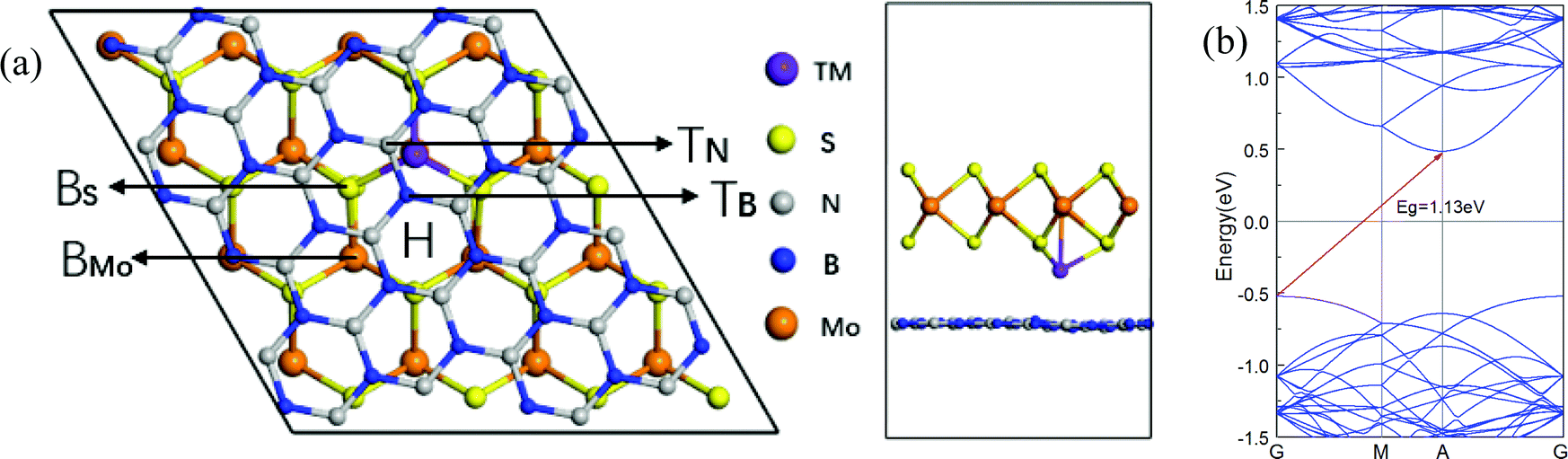 | ||
| Fig. 1 Diagrams showing TM doping in an h-BN/MoS2 heterostructure. Possible initial doping sites before relaxation for TM atoms are marked in the h-BN/MoS2 heterostructure, where BS, BMo, H, TN and TB sites denote below, hollow, and top sites. (a) A top view and side view of the intercalated system. (b) The band structure of the pristine h-BN/MoS2 heterostructure. | ||
The first-principles calculations are performed using the Vienna ab initio simulation package (VASP)35,36 within spin-polarized density functional theory calculation (DFT). The electronic exchange correlation interaction is described within the generalized gradient approximation (GGA) of optimized-Perdew–Burke–Ernzerhof (optPBE-vdW) and the spin orbital coupling (SOC) calculation.37,38 The interactions between the ion core and the valence electrons are modeled with projector-augmented wave (PAW) potentials.39 A plane-wave basis set with a kinetic cutoff energy of 400 eV is employed. The Brillouin zone (BZ) is sampled using 5 × 5 × 1 and 9 × 9 × 1 gamma centered Monkhorst–Pack grids for the calculation of structural relaxation and electronic structures, respectively. The criteria for energy and atom force convergence are set to 10−5 eV per unit cell and 0.01 eV Å−1, respectively.
In order to obtain the most stable absorption positions, the adsorption energies of five different positions are simulated with the following equation:
| Eadsorption = ETM+h-BN/MoS2 − ETM − Eh-BN/MoS2 | (1) |
For analysis of the spin polarization at the Fermi level or Highest Occupied Molecular Orbital (HOMO) level,40,41P(EF) is defined as:
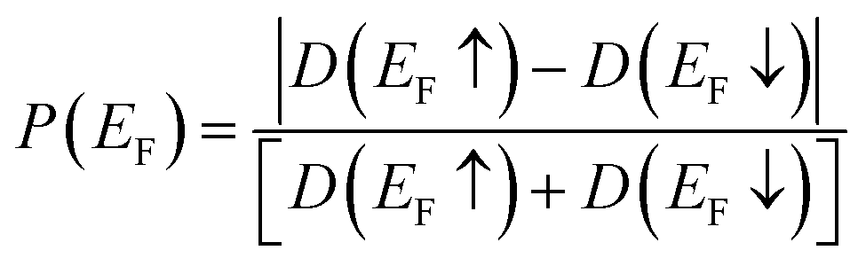 | (2) |
3. Results and discussion
All structures of TM atoms intercalated are based on an optimized h-BN/MoS2 heterostructure whose lattice constant is 13.10 Å, with an indirect bandgap of 1.13 eV, and whose valence band maximum (VBM) and condition band minimum (CBM) are located at the Γ and A points, which is in agreement with previous reports.42,43 Six 3d TM (V, Cr, Mn, Fe, Co and Ni) atoms are chosen to intercalate in the interlayer of the h-BN/MoS2 heterostructure. As shown in Fig. 1, with the symmetry of the h-BN/MoS2 heterostructure, we investigate five possible adsorption positions, i.e. BS (below the S atom), BMo (below the Mo atom), H (the hollow site of the hexagonal structure), TB (on top of the B atom) and TN (on top of the N atom). Finally, by comparing the absorption energies of different adsorption positions, BMo is the lowest for the TM atoms. Interstitial doped TM atoms in the interlayer disturb the lattice configuration of the pristine heterostructure. The absorption energy and the bond length between the TM atoms and four adjacent inherent atoms (Mo, S, B and N) are listed in Table 1. The results indicate that all the intercalated systems behave with chemisorption characteristics because of the negative values of the adsorption energies. The strongest chemisorption cases are the V, Cr, Mn, Fe and Co intercalated systems, and their adsorption energies at the BMo site are −5.15, −5.20, −5.01 and −3.70 eV, respectively. While the Ni atom doping system reveals a weak chemisorption situation with −0.09 eV adsorption energy. The distances between the nearest Mo, S, B and N atoms to the TM atom, are listed in Table 1. And since the TM atoms are doped in the interlayer, the S–Mo bond length of the MoS2 layer is almost decreased slightly because of the stronger bonding interaction between the adjacent S atom and the TM atoms. In order to estimate the intercalated structural stability in practical applications, the molecular dynamics simulation is studied, as shown in Fig. 2(a–c). On a time scale of 2 ps and at a temperature of T = 400 K, although the structure of the Mn-intercalated h-BN/MoS2 heterostructure undergoes a slight structural change, compared with the structure at 0 K, there is no large deformation or atomic bond fracture, indicating that it has thermodynamically stability.| Atom | V | Cr | Mn | Fe | Co | Ni |
|---|---|---|---|---|---|---|
| E ads | −5.15 | −5.20 | −5.01 | −3.70 | −3.17 | −0.90 |
| D TM-Mo/Å | 2.86 | 2.85 | 2.63 | 2.61 | 2.63 | 2.60 |
| D TM-S/Å | 2.37 | 2.39 | 2.28 | 2.19 | 2.16 | 2.17 |
| D TM-B/Å | 2.42 | 2.43 | 2.50 | 2.34 | 2.63 | 2.53 |
| D TM-N/Å | 2.44 | 2.54 | 2.40 | 2.30 | 2.10 | 2.19 |
| D S-Mo/Å | 2.52 | 2.51 | 2.55 | 2.51 | 2.50 | 2.51 |
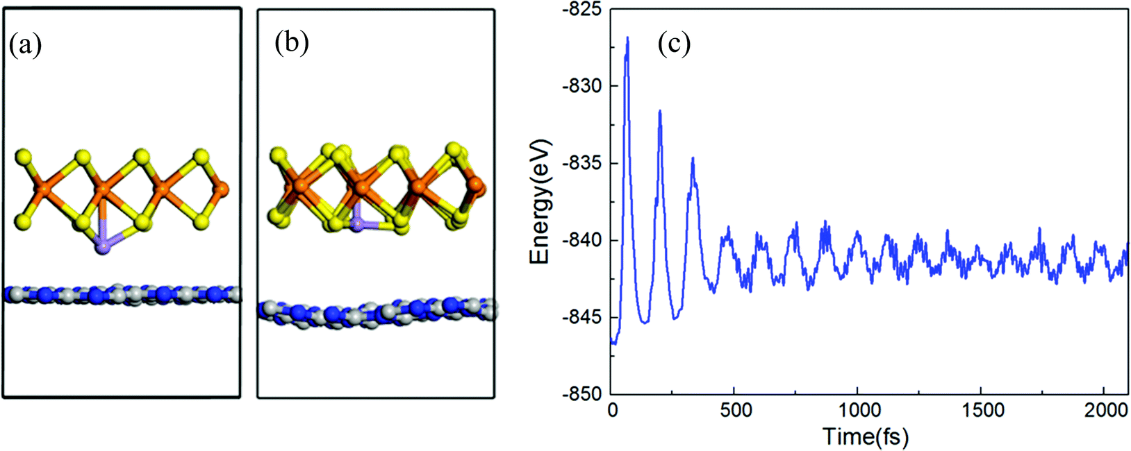 | ||
| Fig. 2 Structural side views of a Mn atom intercalated in the h-BN/MoS2 heterostructure system at (a) 0 K and (b) 400 K. (c) Variation in energy with increasing time obtained from molecular dynamics (MD) simulations at 400 K for a Mn atom intercalated in the interlayers of the h-BN/MoS2 heterostructure system. | ||
The local magnetic moment caused by the intercalation of transition-metal atoms is always the priority of a TM atom intercalated system. To study the magnetic behavior of TM atoms intercalated in the h-BN/MoS2 heterostructure, magnetic moment values of the TM atoms are listed in Table 2. It is clear that the magnetic moments of V, Cr, Mn, Fe and Co after interlayer doping are reduced by 0.23, 3.42, 3.27, 3.02 and 2.42μB, respectively, compared with those of their free-standing states. Nevertheless, the Ni atom intercalated system exhibits no magnetism.
| Atom | μ 0 (μB) | μ (μB) | Te | 4s/3d | 4s*/3d*/4p* | |
|---|---|---|---|---|---|---|
| V | Heterostructure | 3 | 2.77 | 0.57 | 2/3 | 0.34/3.63/0.46 |
| Bilayer MoS2 | 3 | 2.89 | 0.59 | 2/3 | 0.34/3.59/0.48 | |
| Cr | Heterostructure | 6 | 2.58 | 1.10 | 1/5 | 0.24/4.40/0.26 |
| Bilayer MoS2 | 6 | 2.29 | 0.82 | 1/5 | 0.30/4.46/0.42 | |
| Mn | Heterostructure | 5 | 1.73 | 1.26 | 2/5 | 0.25/5.22/0.27 |
| Bilayer MoS2 | 5 | 1.72 | 1.13 | 2/5 | 0.27/5.27/0.33 | |
| Fe | Heterostructure | 4 | 0.98 | 0.92 | 2/6 | 0.32/6.41/0.35 |
| Bilayer MoS2 | 4 | 1.13 | 0.58 | 2/6 | 0.38/6.55/0.49 | |
| Co | Heterostructure | 3 | 0.58 | 0.56 | 2/7 | 0.39/7.58/0.47 |
| Bilayer MoS2 | 3 | 0.57 | 0.48 | 2/7 | 0.40/7.56/0.56 | |
| Ni | Heterostructure | 2 | 0.00 | 0.57 | 2/8 | 0.40/8.58/0.45 |
| Bilayer MoS2 | 2 | 0.00 | 0.50 | 2/8 | 0.40/8.63/0.47 |
To explore the reason for the variation in the magnetic moments of the TM atoms, we calculate the charge transfer between the TM atoms and the h-BN/MoS2 heterostructure owing to band arrangement by using Bader charge analysis.44 As shown in Table 2, the results indicated that there are 0.57, 1.10, 1.26, 0.92, 0.56 and 0.57 electrons transferred from the dopant TM atoms to the h-BN/MoS2 heterostructure. The 3d orbital of the free V atom in the ground state has 3 unpaired electrons with 3μB. When TMs are intercalated in the interlayer of the h-BN/MoS2 heterostructure, the coupling between V and the h-BN/MoS2 heterostructure draws 1.66 electrons out from the 4s orbital and promotes 0.63 electrons into the 3d orbital. However, for the Cr atom doping system, both the 4s orbital and 3d orbital lose electrons, and transfer them to the 4p orbital and heterostructure. Consequently, the unpaired charge of the 4s and 3d orbital decreases, so the magnetic moment value of Cr is reduced from the natural magnetic moment of 6μB to 2.58μB. The 3d orbital of Mn/Fe/Co atoms has 5, 6, 7 electrons, respectively. After electron rearrangement, 0.22, 0.41, and 0.58 electrons transfer from the 4s orbit into the 3d orbital, making 3d orbits of three TM atoms into a half-filled d shell. The magnetic moments of the Mn/Fe/Co atoms are reduced to 1.73, 0.98 and 0.58μB. The Bader charge analysis indicates that there are electron transitions from 4s to 3d states, resulting in a reduction in unpaired electrons and thus lowering their magnetic moments for the V/Mn/Fe/Co atom interlayer intercalation systems. Interestingly, along with the coupling between TM atoms and the h-BN/MoS2 heterostructure, the 4p orbitals of the TMs are filled with sectional electrons from the 4s orbital and 3d orbital. The 3d orbital of the independent Ni atom has 8 electrons, and the Bader charge analysis indicates that 0.58 electrons of the 4s orbital transfer to the 3d orbital. Therefore, the 3d orbital of Ni intercalated in an h-BN/MoS2 heterostructure is almost close to the full shell, showing no magnetic moment. As to V/Fe atom intercalated systems, the variations in magnetic moment in the h-BN/MoS2 heterostructure are larger than those in the MoS2 bilayer, indicating that the coupling effect between the V/Fe intercalated atom and the heterojunction is stronger. It is clear that the amounts of charge transference between intercalary TM atoms (except for V atoms) and the h-BN/MoS2 system are more than those between dopant TM atoms in the interlayer and the MoS2 bilayer, i.e., the substrate h-BN facilitates charge transfer between the intercalated TM atoms and the MoS2 layer.
To visually analyze the strong couplings among the 4s, 4p and 3d orbits, we calculate the partial density of states (PDOS) for the six TMs intercalated systems, as shown in Fig. 3. According to the PDOS of transition metal atoms, the asymmetric DOS peaks only appear in the cases of V-, Cr-, Mn-, Fe-, and Co-intercalation, whose systems are magnetic. However, the density of state is symmetric about spin-up and spin-down electrons and there is no magnetism for the Ni-doped system. The results of magnetization also show that magnetic moment for the whole system is mainly attributed to magnetization of the metal atom. For the V atom intercalated system, the valence band is mainly comprised of 4s, 4p and 3d state coupling, and the conduction band mainly is contributed by 3d states. Furthermore, it is clear that there exists orbital coupling between 4s and the 3d in the valence band for the Cr and Mn systems. For the Fe intercalated system, the 3d orbital is the dominant state of the conduction band. The conclusions reflected from the PDOS are matched with the above results of Bader charge analysis. The magnetic moment is determined mainly by the 3d orbital of different TM atoms.
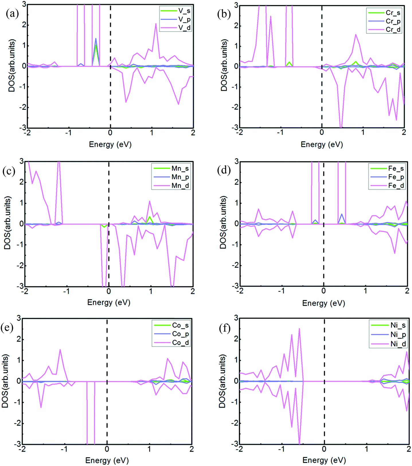 | ||
| Fig. 3 The partial density of states (PDOS) projected onto the atomic orbitals of the TM atoms. For (a) V, (b) Cr, (c) Mn, (d) Fe, (e) Co, and (f) Ni, the chosen orbitals are the 4s, 4p and 3d orbitals of the TM. The green, blue and magenta lines denote 4s, 4p, and 3d, respectively. The dotted line is the Fermi level, set as 0 eV. The upper panels present the majority spin, and the lower panels are the minority spin. | ||
In order to evaluate the bonding characters and charge transfer situation of the h-BN/MoS2 heterostructure with intercalated TMs, the charge density difference is further studied, as demonstrated in Fig. 4. All the intercalated TMs are closer to the MoS2 layer than to the h-BN layer, and the charge accumulation space appears at the interlayer of the MoS2 layer near the TM atoms resulting from the stronger bonding effect between S atoms and TM atoms. However, there is no significant charge transition between the layers of the vdW heterostructure. Fig. 4 shows that there are obvious 3d orbital nodes around the TM atoms, which indicates that the charge density of the 3d orbital increases. Meanwhile, the 0.75 difference in electronegativity between all of the TM atoms and S atoms is much smaller than 1.7, which is the critical value to distinguish the type of bond,45 demonstrating that the covalent-bonding character occurs in the region between the TM atoms and the S atoms.
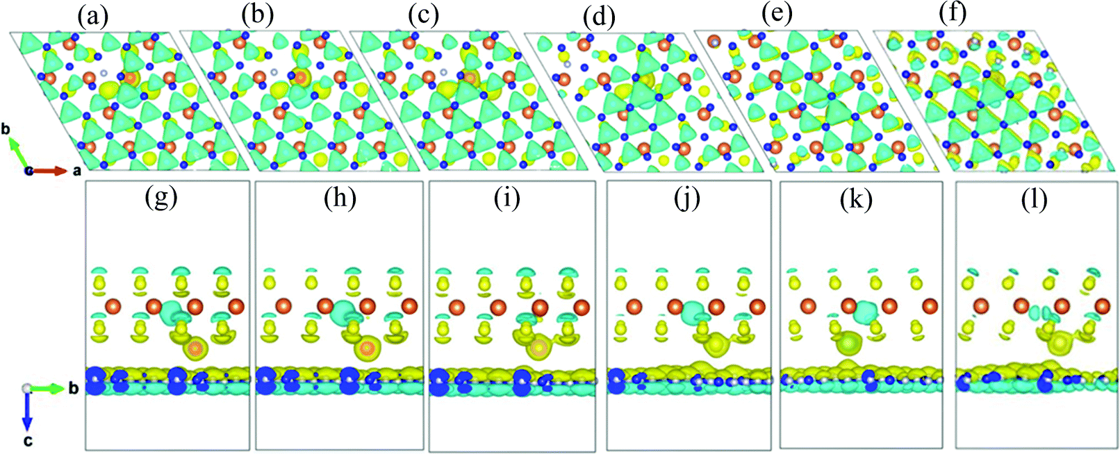 | ||
| Fig. 4 The charge density difference distributions for (a, g) V, (b, h) Cr, (c, i) Mn, (d, j) Fe, (e, k) Co, and (f, l) Ni. The yellow and blue regions refer to electron accumulation and depletion, respectively. | ||
Spin-resolved band structures of respective TMs doped in the interlayer of the h-BN/MoS2 heterostructure with GGA and GGA + SOC calculation are all performed in Fig. 5. By comparing the calculation results, it can be seen that the SOC has little influence on the energy band structure, except that the energy band gap varies slightly with applied SOC calculation. Fig. 5(a–f) are the band structures of six systems intercalated with TM atoms. The systems intercalated with V and Cr atoms (Fig. 5(a and b)) transfer from a spin-degenerated indirect bandgap semiconductor to metallic properties. When SOC is taken into the calculation, the V and Cr intercalated systems still exhibit a metallic nature and the impurity state shows a slight upward shift. For the Mn, Fe and Co intercalated cases, all of them are still semiconductors while the bandgaps of the three interlayer dopant systems become narrow, and the bandgaps of the Mn, Fe and Co intercalated systems with SOC increase to 0.12, 0.29 and 0.18 eV, respectively. Meanwhile, they exhibit 100% spin polarization at the HOMO level, which is significant for the design of spintronic and optoelectronic devices. In addition, the Ni atom intercalated system narrows its bandgap to 0.81 eV in both cases. The consequence is different from the result of bilayer MoS2 intercalated with 3d TMs, in which the intercalary Cr and Fe systems exhibit half-metallic behavior, and the other 3d TMs intercalated systems are magnetic semiconductors except for Ni species,46 which shows that the heterogeneous h-BN sheet plays a role in the electronic property. All of the above results indicate that the TM atoms intercalated in the interlayer of an h-BN/MoS2 heterostructure is an effective modulation approach for their electronic properties.
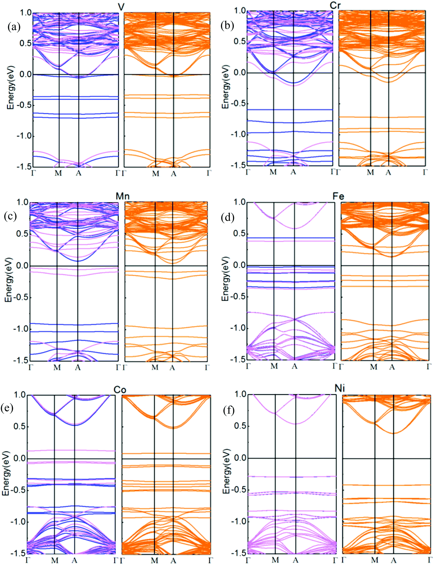 | ||
| Fig. 5 The band structures of TM atoms ((a) V, (b) Cr, (c) Mn, (d) Fe, (e) Co, and (f) Ni) doped into the interlayers of the h-BN/MoS2 heterostructure without SOC calculations (the blue and red curves on the left-hand side), and with SOC calculations (the orange curves on the right-hand side). | ||
4. Conclusions
In summary, we investigated whether intercalated TM atoms and h-BN layers would have an effect on the electronic and magnetic properties of h-BN/MoS2 heterostructures via first-principles calculations. It is clear that, except for the h-BN/MoS2 heterostructure system with intercalated Ni atoms, the other (V, Cr, Mn, Fe, and Co) intercalated systems induce magnetic moments. After the TM atom has intercalated into the h-BN/MoS2 heterostructure, the magnetic moments of the six TM atoms decrease compared with their free-standing states. The variation in magnetic moment derives from charge exchange between the 4s and 3d states of the TMs according to Bader charge analysis. Taking the example of the intercalated Mn atom system, it is thermodynamically stable at 400 K based on molecular dynamics simulations. Via comparing with TMs doped in the interlayers of a bilayer MoS2 structure, we found that the h-BN layers have a positive facilitation effect on charge transfer with respect to the intercalated TM atoms. The band structure is very sensitive to interlayer interactions in the h-BN/MoS2 heterostructure. The intercalating V and Cr systems exhibit metallic nature, while the other still behave as semiconductors and the spin polarization is 100% at the HOMO level, which means they can be used as potential materials for spintronic devices.Conflicts of interest
There are no conflicts to declare.Acknowledgements
This work was supported by the grants from the National Natural Science Foundation of China (No. 11504312), Provincial Natural Science Foundation of Hunan (No. 2019JJ50612), Open Fund based on innovation platform of Hunan colleges and universities (No. 18K032), Scientific Research Fund of Hunan Provincial Education Department (No. 18A059), Hunan Key Laboratory of Two-Dimensional Materials (No. 2018TP1010), the Program for Changiang Scholars and Innovative, and the Program for Changjiang Scholars and Innovative Research Team in University (IRT_17R91).References
- A. K. Geim and I. V. Grigorieva, Nature, 2013, 499, 419–425 CrossRef CAS PubMed.
- K. S. Novoselov, A. Mishchenko, A. Carvalho and A. H. C. J. S. Neto, Science, 2016, 353, 94391–943911 CrossRef PubMed.
- Y. Liu, N. O. Weiss, X. Duan, H. Cheng, Y. Huang and X. Duan, Nat. Rev. Mater., 2016, 1, 16042 CrossRef CAS.
- C. Wang, J. Sun, B. Zhang, J. Zhang and X. Tao, Appl. Surf. Sci., 2017, 423, 1003–1011 CrossRef CAS.
- J. Slawinska, I. Zasada and Z. Klusek, Phys. Rev. B: Condens. Matter Mater. Phys., 2010, 81, 155433 CrossRef.
- K. Kośmider and J. Fernández-Rossier, Phys. Rev. B: Condens. Matter Mater. Phys., 2013, 87, 070451 CrossRef.
- S. J. Zhang, C. W. Zhang, S. F. Zhang, W. X. Ji, P. Li, P. J. Wang, S. S. Li and S. S. Yan, Phys. Rev. B, 2017, 96, 205433 CrossRef.
- L. Kou, T. Frauenheim and C. Chen, J. Phys. Chem. Lett., 2013, 4, 1730–1736 CrossRef CAS PubMed.
- H. Wang, F. Liu, W. Fu, Z. Fang, W. Zhou and Z. Liu, Nanoscale, 2014, 6, 12250–12272 RSC.
- M. Bernardi, M. Palummo and J. C. Grossman, Nano Lett., 2013, 13, 3664–3670 CrossRef CAS PubMed.
- B. Radisavljevic, A. Radenovic, J. Brivio, V. Giacometti and A. Kis, Nat. Nanotechnol., 2011, 6, 147–150 CrossRef CAS PubMed.
- G. Liu, S. L. Rumyantsev, C. Jiang, M. S. Shur and A. A. Balandin, IEEE Electron Device Lett., 2015, 36, 1202–1204 CAS.
- A. D. Bykhovski, R. Gaska and M. S. Shur, Appl. Phys. Lett., 1998, 73, 3577–3579 CrossRef CAS.
- W. Zan, W. Geng, H. Liu and X. Yao, Phys. Chem. Chem. Phys., 2016, 18, 3159–3164 RSC.
- M. Hetzl, M. Kraut, J. Winnerl, L. Francaviglia, M. Doblinger, S. Matich, F. I. M. Anna and M. Stutzmann, Nano Lett., 2016, 16, 7098–7106 CrossRef CAS PubMed.
- C. W. Zhang and S. S. Yan, Appl. Phys. Lett., 2009, 95, 153 Search PubMed.
- Y. Wu, Z. Huang, H. Liu, C. He, L. Xue, X. Qi and J. Zhong, Phys. Chem. Chem. Phys., 2018, 20, 17387–17392 RSC.
- Y. Liu, J. Sheng, H. Wu, Q. He, H. C. Cheng, M. I. Shakir, Y. Huang and X. Duan, Adv. Mater., 2016, 28, 4120 CrossRef CAS PubMed.
- B. W. Veal, S. K. Kim, P. Zapol, H. Iddir, P. M. Baldo and J. A. Eastman, Nat. Commun., 2016, 7, 11892 CrossRef CAS PubMed.
- M. G. Menezes, R. B. Capaz and J. L. B. Faria, Phys. Rev. B: Condens. Matter Mater. Phys., 2010, 82, 245414 CrossRef.
- F. Shojaei, J. R. Hahn and H. S. Kang, J. Phys. Chem. C, 2016, 120, 17106–17114 CrossRef CAS.
- Y. Guang, Y. Ma, H. Mao, X. Li and C. Jie, Nanotechnology, 2018, 29, 115201 CrossRef PubMed.
- Y. Gong, H. Yuan, C. L. Wu, P. Tang, S. Z. Yang, A. Yang, G. Li, B. Liu, V. D. G. Jorik and M. L. Brongersma, Nat. Nanotechnol., 2018, 13, 294–299 CrossRef CAS PubMed.
- F. Lévy, Phys. Chem. Mater. Layered Struct., 1979, 6, 323–421 Search PubMed.
- S. P. Koenig, R. A. Doganov, L. Seixas, A. Carvalho, J. Y. Tan, K. Watanabe, T. Taniguchi, N. Yakovlev, A. H. Castro Neto and B. Zyilmaz, Nano Lett., 2016, 16, 2145–2151 CrossRef CAS PubMed.
- Z. Chen, K. Leng, X. Zhao, S. Malkhandi, W. Tang, B. Tian, L. Dong, L. Zheng, M. Lin and B. S. Yeo, Nat. Commun., 2017, 8, 14548 CrossRef CAS PubMed.
- X. C. Liu, S. Zhao, X. Sun, L. Deng and P. M. Ajayan, Sci. Adv., 2020, 6, eaay4092 CrossRef CAS PubMed.
- Y. Gong, H. Yuan, C. L. Wu, P. Tang, S. Z. Yang, A. Yang, G. Li, B. Liu, V. D. G. Jorik and M. L. Brongersma, Nat. Nanotechnol., 2018, 13, 294–299 CrossRef CAS PubMed.
- X. Zhao, P. Song, C. Wang, A. C. Riis-Jensen and K. P. Loh, Nature, 2020, 581, 171–177 CrossRef CAS PubMed.
- E. C. T. O'Farrell, J. Y. Tan, Y. Yeo, G. K. W. Koon, B. Ãzyilmaz, K. Watanabe and T. Taniguchi, Phys. Rev. Lett., 2016, 117, 076603 CrossRef PubMed.
- M. H. Zhang, C. W. Zhang, P. J. Wang and S. S. Li, Nanoscale, 2018, 10, 20226–20233 RSC.
- T. Ahmed, N. A. Modine and J. Zhu, Mater. Sci., 2015, 15, 07398 Search PubMed.
- C. Wang, J. Sun, B. Zhang, J. Zhang and X. Tao, Appl. Surf. Sci., 2017, 423, 1003–1011 CrossRef CAS.
- Y. Wang, X. Song, N. Song, T. Zhang, X. Yang, W. Jiang and J. Wang, RSC Adv., 2019, 9, 19418 RSC.
- G. Kresse and J. Furthmüller, Comput. Mater., 1996, 6, 15–50 CrossRef CAS.
- G. Kresse and J. Furthmüller, Phys. Rev. B: Condens. Matter Mater. Phys., 1996, 54, 11169–11186 CrossRef CAS PubMed.
- G. F. Dresselhaus, Phys. Rev., 1955, 100, 580–586 CrossRef CAS.
- J. R. Elliott, Phys. Rev., 1954, 96, 266–279 CrossRef.
- P. E. Blöchl, Phys. Rev. B: Condens. Matter Mater. Phys., 1994, 50, 17953 CrossRef PubMed.
- Y. Mao and J. Zhong, Nanotechnology, 2008, 19, 205708 CrossRef PubMed.
- E. Durgun and S. Ciraci, Phys. Rev. B: Condens. Matter Mater. Phys., 2006, 74, 125404 CrossRef.
- R. Gillen, J. Robertson and J. Maultzsch, Phys. Rev. B: Condens. Matter Mater. Phys., 2014, 90, 075437 CrossRef CAS.
- F. F. Yu, S. S. Ke, S. S. Guan, H. X. Deng, Y. Guo and L. Hai-Feng, Phys. Chem. Chem. Phys., 2019, 21, 20073–20082 RSC.
- G. Henkelman, A. Arnaldsson and J. Hannes, Comput. Mater. Sci., 2006, 36, 354–360 CrossRef.
- L. Jones and P. Atkins, Chemistry: molecules, matter, and change. New York: W.H. Freeman and Company, pp. 294–295, 1997 Search PubMed.
- X. Q. Wang, W. G. Chen, Z. L. Zhu and Y. Jia, Acta Metall. Sin., 2015, 28, 793–798 CrossRef CAS.
| This journal is © the Owner Societies 2021 |