
 Open Access Article
 This Open Access Article is licensed under a Creative Commons Attribution-Non Commercial 3.0 Unported Licence
Morphological characterization and electronic properties of pristine and oxygen-exposed graphene nanoribbons on Ag(110)
Jose Eduardo
Barcelon
ab,
Marco
Smerieri
a,
Giovanni
Carraro
ac,
Pawel
Wojciechowski
de,
Luca
Vattuone
 ac,
Mario
Rocca
*ac,
Silvia
Nappini
f,
Igor
Píš
fg,
Elena
Magnano
fh,
Federica
Bondino
f,
Luca
Vaghi
i,
Antonio
Papagni
i and
Letizia
Savio
*a
ac,
Mario
Rocca
*ac,
Silvia
Nappini
f,
Igor
Píš
fg,
Elena
Magnano
fh,
Federica
Bondino
f,
Luca
Vaghi
i,
Antonio
Papagni
i and
Letizia
Savio
*a
aIMEM-CNR, UOS Genova, Via Dodecaneso 33, 16146 Genova, Italy. E-mail: letizia.savio@imem.cnr.it; rocca@fisica.unige.it
bDipartimento di Scienze Chimiche, della Vita e della Sostenibilità Ambientale Università di Parma, Parco Area delle Scienze, 17/A, 43124 Parma, Italy
cDipartimento di Fisica, Università degli Studi di Genova, Via Dodecaneso 33, 16146 Genova, Italy
dInstitute of Molecular Physics, Polish Academy of Sciences, M. Smoluchowskiego 17, 60-179 Poznań, Poland
eNanoBioMedical Centre, Adam Mickiewicz University, Wszechnicy Piastowskiej 3, 61-614 Poznań, Poland
fIOM CNR laboratorio TASC, 34149 Basovizza (TS), Italy
gElettra-Sincrotrone Trieste S.C.p.A., 34149 Basovizza (TS), Italy
hDepartment of Physics, University of Johannesburg, PO Box 524, Auckland Park 2006, South Africa
iDipartimento di Scienza dei Materiali, Università di Milano-Bicocca, Via R. Cozzi 55, 20125 Milano, Italy
First published on 21st December 2020
Abstract
Graphene nanoribbons (GNRs) are at the frontier of research on graphene materials since the 1D quantum confinement of electrons allows for the opening of an energy gap. GNRs of uniform and well-defined size and shape can be grown using the bottom-up approach, i.e. by surface assisted polymerization of aromatic hydrocarbons. Since the electronic properties of the nanostructures depend on their width and on their edge states, by careful choice of the precursor molecule it is possible to design GNRs with tailored properties. A key issue for their application in nanoelectronics is their stability under operative conditions. Here, we characterize pristine and oxygen-exposed 1.0 nm wide GNRs with a well-defined mixed edge-site sequence (two zig-zag and one armchair) synthesized on Ag(110) from 1,6-dibromo-pyrene precursors. The energy gap and the presence of quantum confined states are investigated by scanning tunneling spectroscopy. The effect of oxygen exposure under ultra-high vacuum conditions is inferred from scanning tunneling microscopy images and photoemission spectra. Our results demonstrate that oxygen exposure deeply affects the overall system by interacting both with the nanoribbons and with the substrate; this factor must be considered for supported GNRs under operative conditions.
Introduction
Graphene, a carbon allotrope consisting of a single layer of sp2 hybridized carbon atoms in a honeycomb lattice, shows relevant mechanical, electronic and optical properties (e.g. high intrinsic charge mobility, high electrical and thermal conductivity, high optical transparency and high tensile strength), which made it a promising material for several applications. However, while some of these properties (including excellent ballistic transport of charge carriers) make graphene suitable for devices where high electrical conductivity is mandatory (e.g. electrodes), the absence of a gap prevents its use in nanoelectronics, for which a semiconducting behaviour is required.For this reason, the attention moved on low-dimensional graphene-based nanostructures such as carbon nanotubes and graphene nanoribbons (GNRs). The latter are graphene-like, one-dimensional (1D) nanostructures narrower than 10 nm.1–5 They are of particular interest because the quantum confinement of the electrons and the presence of different edge geometries (with possible associated electronic states) cause a bandgap opening, while still retaining the ballistic transport of charge carriers.
GNRs can be synthesized using several top-down methods, which include sonication,1 lithography6 and unzipping of carbon nanotubes (CNTs).7,8 These approaches allow for a relatively easy production of graphenic, low dimensional nanostructures which, however, often have a relatively poor quality in terms of uniformity and defectivity at the edges. Since regularity of shape and size is required for a variety of applications, and in particular for nanoelectronics, the alternative bottom-up approach appears more promising.9–12 It usually exploits the surface assisted polymerization of a molecular precursor (often a halogenated aromatic compound) catalyzed by a metal surface; the process occurs in two steps since Ullman-coupling is followed by cyclodehydrogenation and formation of new C–C bonds.13–16
One of the first precursor molecules to be successfully employed was 10,10′-dibromo-9,9′-bianthracene (DBBA), which polymerizes forming N = 7 GNRs with armchair edges.11 Eventually, a wide variety of halogenated and non-halogenated aromatic hydrocarbons17,18 has been employed to synthesize GNRs with well-defined width and edge sites, either armchair, zig-zag,19 mixed12 or cove.17 Chiral GNRs could also be produced starting from DBBA on Cu(111).10
The final product depends, indeed, on several factors, including the nature and geometry of the metallic substrate11,20,21 and the structure of the precursor molecule.10–12,17,22–24 The choice of the proper compound is essential, since not all possible candidates are suitable and/or stable enough on the surface to allow for the dehydrogenation and C–C coupling processes leading to the formation of extended graphenic nanostructures. As an example, we mention the case of 1,5 di-bromo-tetracene (DBT) and 1,6 di-bromo-pyrene (DBP), two halogenated aromatic hydrocarbons with similar molecular weight and different geometry: some of us produced ordered arrays of GNRs on Ag(110) from DBP polymerization,12 while desorption prevails for DBT on the same substrate.25 On the other hand, the use of Br-corannulene on Ag(110) leads to the formation of C-based ribbons which do not have the spectroscopic signature of graphene because of the non-planar geometry of the precursor molecule.24
It is therefore possible to engineer GNRs (and C-based nanostructures in general) of desired final geometry, and thus tailored electronic properties, by selecting suitable precursor molecules. Energy gaps may then range from close to zero up to almost 3 eV19,23,26,27 depending on the width of the nanoribbons and on whether they present armchair (AGNRs) or zigzag (ZGNRs) edge sites. For AGNRs, the band gap depends on the ribbon width and the nanostructures can be classified in three groups yielding large, medium or small bandgap, respectively.23 On the contrary, ZGNRs have edge states associated with the zig-zag edge sites,19 for which a nearly flat dispersion and a magnetic behaviour are predicted.23 The determination of their electronic properties is therefore a pivotal task for the characterization of such nanostructures.
Another important issue is the chemical activity of GNRs. They are expected to be inert since their edges are saturated with hydrogen but, as in the case of graphene, their reactivity can be enhanced by doping with heteroatoms,16,28 thus opening perspectives in the fields of sensoristics and nano-catalysis.
Independently of their use, GNRs need to be stable under operative conditions. This implies, most often, after-growth exposure to air or a liquid solution and, possibly, their transfer from the native metal substrate to a more suitable substrate for the desired application. In this respect, we mention that GNRs can be successfully transferred with techniques similar to those employed for graphene films.29 For 7- and 9-AGNRs produced under ultra-high vacuum (UHV) conditions, the transfer process does not modify the morphology of the nanostructures. On the contrary, bottom-up synthesis of 7-AGNRs under less stringent, high vacuum (HV) conditions (P = 10−6 mbar)30 is deeply affected by the presence of a residual partial pressure of water and oxygen. For these reasons, understanding at the fundamental level of the interaction of these nanostructures with atmospheric gases is a first step necessary to predict the structure and electronic properties of the nanoribbons under operative conditions and, if transfer from the native substrate is required, how these properties are affected by the substrate change.
Our manuscript deals with this field of research. In a previous Scanning Tunnelling Microscopy (STM) and Density Functional Theory (DFT) analysis, some of us demonstrated that mixed edge-sites GNRs synthesised on Ag(110) from DBP precursors have a very uniform width of 1.0 nm and a well-defined geometry alternating two zig-zag and one armchair site.12 Here, we complete their characterization by unravelling the semiconducting nature of the nanostructures through Scanning Tunnelling Spectroscopy (STS) measurements and we assess how the system is modified by exposure to oxygen in high vacuum conditions, as a first step towards understanding the behaviour of GNRs under realistic conditions. We measure a gap opening compatible with the one expected for graphene nanostructures of similar size and we report a double effect of oxygen exposure: it weakens the interaction of GNRs with the substrate by intercalation and formation of C![[double bond, length as m-dash]](https://www.rsc.org/images/entities/char_e001.gif) O bonds and it also causes a partial modification of the Ag(110) surface morphology with the formation of Ag–O complexes. The overall modification of the system must therefore be considered when exposing supported GNRs to reactive gases.
O bonds and it also causes a partial modification of the Ag(110) surface morphology with the formation of Ag–O complexes. The overall modification of the system must therefore be considered when exposing supported GNRs to reactive gases.
Experimental
Experiments were performed in three different UHV chambers equipped either for Low Temperature Scanning Tunneling Microscopy or for X-Ray Photoemission Spectroscopy (XPS).The first setup consists of a preparation chamber, equipped with an evaporator for organic molecules, gas inlets, a quadrupole mass spectrometer and an ion gun for sample cleaning, and of a main chamber hosting the low temperature Scanning Tunneling Microscope (LT-STM manufactured by Createc) for STM and STS measurements.
The base pressure in the chamber is better than 1 × 10⁻⁹ mbar but, since the LT-STM is totally shielded by a cold screen either at liquid nitrogen (LN2, 77 K) or liquid helium temperature (LHe, 4 K), the pressure at the scanner is much better and allows data acquisition on the same preparation for several days without significant sample contamination. STM images were recorded either at LN2 or LHe temperature, using a Pt/Ir tip cut under strain for the set of experiments performed to determine the surface morphology and a chemically etched tungsten (W) tip for STS measurements. In all cases the tip was repeatedly reshaped by controlled crashes into the surface, so that tunneling occurs effectively through an Ag-coated tip.
STM images were acquired in constant current mode, with a typical tunneling current of 0.1 nA < I < 1.0 nA and a bias voltage −1.5 V < V < 1.5 V applied to the sample. No significant interaction between tip and sample was observed under these conditions, suggesting an overall stability of the system.
Surface orientation and image size were calibrated from atomically resolved images of the clean Ag(110) surface (see inset of Fig. 1A) or of the (nx1)-O–Ag(110) added row reconstruction.31,32 Similarly, heights were calibrated on monatomic Ag steps.
 | ||
| Fig. 1 Left: STM image (V = −150 meV, I = 0.3 nA) showing the co-existence of three different self-assembled structures (labelled as A, B, C) upon deposition of a sub-monolayer of DBP on Ag(110) at RT. Top and bottom insets report, respectively, the molecular structure of DBP and the atomically resolved image of clean Ag(110) from which the high symmetry directions (marked by arrows) are determined (image size: 1.8 × 1.6 nm2). Top right: enlarged image of each domain (either from the area in the overview or from neighbouring areas). Among B domains, it is possible to distinguish rectangular (B1) and rhomboidal unit cells (B2). Empirical models deduced from the periodicities of the self-assembled structures and from XPS results are superimposed to the STM image for structures A, B1 and B2 (grey: de-brominated pyrene units; blue: Ag adatoms; red: Br atoms). Bottom right: line scans cut across the paths marked in the overview for structures A and B1 (follow colour code). Line scans drawn along and across the rows of structure B2 are not reported since they do not differ significantly from those of B1. The higher and sharper features in traces 1 and 3 correspond to the Ag atoms within the organometallic chains. | ||
STS spectra and dI/dV maps were recorded at LHe temperature to minimize thermal drift. The bias range −0.5 V< V < 0.5 V was chosen to measure the gap of the GNRs and the relevant states within it with sufficient signal-to noise ratio and without appreciable drift of the sample. The range for dI/dV maps was then extended to −1.0 V< V < 1.0 V.
Data acquisition was performed using the STM-AFM software (ver. 3,1 provided by Createc). Images were processed using WSxM33 (version 9.4).
High-resolution synchrotron radiation XPS measurements on pristine nanostructures were performed at the BACH beamline of CNR at the Elettra synchrotron radiation source facility (Trieste, Italy). The samples were prepared and measured in an UHV chamber with a base pressure lower than 1 × 10⁻⁹ mbar. The XPS spectra were collected using a hemispherical electron energy analyser (VG Scienta, model R3000) at an angle of 60° with respect to the X-ray incidence beam direction and at an emission angle of 60° from the surface normal. Br 3d and C 1s core levels were acquired with 277 and 379 eV photon energy, respectively. The binding energies are referenced to the substrate Fermi edge. The energy resolution of 0.15 eV was determined from the width of the Fermi edge. The C 1s spectra were fitted with slightly asymmetric Doniach-Sunjic line shapes convoluted with the Gaussian profile.34,35 A Shirley type background was applied.
XPS spectra of the oxygen-exposed GNRs were acquired in a third UHV apparatus, equipped with a conventional, non-monochromatized AlKα X-ray source and hemispherical analyzer (Omicron, DAR400 and EA125). Spectra were recorded at normal emission and calibrated to a binding energy of the Ag 3d5/2 line of 368.25 eV.
Sample preparation
For the present experiments 1,6-Dibromopyrene (see inset in Fig. 1 for the molecular structure) was synthesized as described in ref. 12.The samples were prepared in situ in each experimental chamber. The Ag(110) surface was cleaned by cycles of sputtering with noble gas ions (either Ne+ or Ar+ with 1 to 3 keV kinetic energy) followed by prolonged annealing to T = 550 °C or T ∼ 400 °C for microscopy and photoemission experiments, respectively. Surface cleanliness and order were checked by STM or by XPS and low energy electron diffraction.
DBP molecules were sublimated on the clean metal surface at room temperature (RT) from a Tantalum crucible heated to 70 °C–100 °C under UHV until a coverage of DBP on Ag(110) of (0.6 ± 0.2) ML was obtained, as estimated by XPS and STM. Sub-monolayer coverage is chosen in order to have some bare Ag(110) areas after GNRs polymerization, a condition preferable both for STS inspection and for better evidencing the effect of O2 exposure.
After DBP deposition, the sample was stepwise annealed to produce GNRs, following the protocol defined in ref. 12: firstly, the sample was slowly heated to T = 150 °C and kept at such temperature for 15 min. Then, the temperature was raised to 400 °C (350 °C for XPS experiments at BACH) for 5 min and eventually slowly cooled down.
GNRs were subsequently exposed to O2 at RT or 300 °C for 20 min at a background pressure P = 1 × 10⁻⁶ mbar, resulting in a nominal exposure of 900 L. Since a doser placed at ∼2 cm from the sample surface was employed, we estimate a local enhancement of the pressure by approximately a factor of 5.36
At each stage of the preparation the sample was cooled down to LN2 temperature and inserted eventually into the LT-STM for inspection. Conversely, XPS spectra were recorded with the sample at RT.
Results and discussion
(i) DBP/Ag(110) at RT
Upon deposition of a sub-monolayer of DBP at RT, the precursor molecules self-assemble into large islands, often covering the whole terrace, and organize in domains with different geometries. Such behavior denotes a large mobility of the precursor molecules at RT.The overview in Fig. 1 shows the co-existence of three different self-assembled structures (denoted as A, B, C in the image), which are better detailed in the enlargements on the right-hand side of the figure. Among B domains, it is possible to distinguish rectangular (B1) and rhomboidal unit cells (B2), shown in the top right panel. Structures A, B1 and B2 form ordered patterns with specific periodicities, as shown in the line scans in the bottom panel. Structure C presents a less regular assembly; it appears less frequently and it is found in small domains at the border between domains of type A and B.
Structure A consists of straight rows oriented, within experimental error, along the 〈1![[1 with combining macron]](https://www.rsc.org/images/entities/char_0031_0304.gif) 0〉 direction. Nearly oval features alternate to small, bright dots; statistical analysis over several line scans, as the one reported in the bottom panel, yields a periodicity of (8.4 ± 0.9) Å (trace 1, blue) and (9.0 ± 0.4) Å (trace 2, red) along and across the rows, respectively, from which we infer a local molecular density of ∼1.3 × 10¹⁴ DBP units per cm2. These periodicities suggest that each of the large roundish protrusions in the chain consists of one single DBP unit. Additional bright small features are also present in-between the rows, the nature of which is discussed in the following.
0〉 direction. Nearly oval features alternate to small, bright dots; statistical analysis over several line scans, as the one reported in the bottom panel, yields a periodicity of (8.4 ± 0.9) Å (trace 1, blue) and (9.0 ± 0.4) Å (trace 2, red) along and across the rows, respectively, from which we infer a local molecular density of ∼1.3 × 10¹⁴ DBP units per cm2. These periodicities suggest that each of the large roundish protrusions in the chain consists of one single DBP unit. Additional bright small features are also present in-between the rows, the nature of which is discussed in the following.
Structure B consists of chains alternating a larger protrusion, identified with a DBP unit, with a smaller and brighter one. One or two additional spots per each DBP unit are present in-between the rows. At variance with structure A, these chains are oriented at either −35° or 88° off 〈10〉 and they are rather bent than straight. The less regular geometry causes the DBP units in adjacent rows to be either aligned, giving rise to a rectangular unit cell (assembly B1), or misaligned, resulting in a rhomboidal unit cell (assembly B2). Statistical analysis over high-resolution images of structure B allowed to determine an average periodicity of (9.9 ± 0.5) Å along the rows (trace 3, violet) and (8.7 ± 0.5) Å across the rows (trace 4, green), corresponding to a local molecular density of ∼1.2 × 10¹⁴ DBP units per cm2.
XPS was used to determine the possible chemical nature of the self-assembled DBP layer. Upon deposition of 0.6 ML of DBP on Ag(110) at RT (bottom spectra in Fig. 2a and b), the Br 3d spectral region shows the presence of a major Br moiety evidenced by the 3d doublet with Eb(Br 3d5/2) = 68.2 eV and a minority one with Eb(Br 3d5/2) = 70.4 eV. The latter component is ascribed to Br–C bonds in the intact DBP molecules, as substantiated by comparison with the corresponding experiment performed at 1.2 ML DBP coverage12 and by other experiments performed on the less reactive Au(111) surface.37,38 The lower Eb species corresponds, on the other hand, to Br atoms chemisorbed on the Ag substrate and its higher intensity indicates an almost complete debromination of the DBP admolecules at RT. This picture is confirmed by inspection of the C 1s spectrum. The main peak at Eb ∼ 284.3 eV corresponds to the aromatic carbon rings. In addition, a weaker but clearly visible component is present at 283.1 eV, which is a typical fingerprint of C–Ag bonds that are formed when metal adatoms from the substrate react with carbon radicals. This is, therefore, a signature that breaking of the C–Br bond has occurred25,39 and that DBP-Ag organometallic chains have formed. Peak decomposition analysis reveals that the main peak results from the superposition of at least three unresolved components. The relative intensities indicate that the two components at ∼284.1 and ∼284.5 eV could be assigned to carbon atoms bound only to carbon and to carbon atoms bound to carbon and hydrogen, respectively. The third component at Eb ∼ 285.2 eV is rather weak and we ascribe it to Br–C bonds. In accordance with Br 3d spectra, it disappears after a short mild annealing or after some hours at room temperature (not shown). In this respect we must note that the relative integrated intensity of the C–Ag component with respect to the total C 1s peak area (0.06) is about half of the value expected for complete substitution of all the C–Br bonds with C–Ag bonds (0.125). Thus, XPS data suggest that at sub-monolayer coverage and RT the large majority of the DBP molecules undergo complete debromination and that the detached Br atoms are adsorbed on the substrate, but that not all the broken C bonds are saturated by Ag. This can be explained by the formation of surface stabilized pyrene radicals or biradicals adsorbed in conformations not favorable for bonding with the Ag adatoms. Formation of covalent bonds between the pyrene derivatives is less probable in view of the morphology observed by STM and of the models proposed in the following.
 | ||
| Fig. 2 (a) Br 3d and (b) C 1s core level spectra of 0.6 ML of DBP deposited on Ag(110) at RT and after annealing the sample to the indicated temperature for 5 min. (c) Normalized integrated intensity of Br 3d and C 1s peaks as a function of temperature. The intensities are normalized to the peak areas measured after the deposition. | ||
The XPS information is valuable for a complete interpretation of the STM image of Fig. 1, since it allows to identify the small bright features present in and in-between the rows. Therefore, by analogy with what observed for a DBP multilayer annealed to 150 °C,12 we propose that the de-brominated molecules form organometallic chains with Ag adatoms provided by the sample, most probably released from the steps,32 while dissociated Br atoms sit in-between these chains. So, the empirical models superimposed to the enlargements in Fig. 1 are proposed: the bright dots in the chains are Ag atoms (blue circles) bound to the pyrene groups to form organometallic proto-polymers and the Br atoms occupy interstitial sites in-between the rows (red circles).
(ii) Synthesis and characterization of GNRs
The preparation reported in Fig. 1 was eventually annealed following the protocol described in ref. 12 and summarized in the experimental section, in order to induce the synthesis of GNRs by surface assisted polymerization (Fig. 3a). The so-produced sample was then exposed to oxygen at RT and at T = 300 °C (Fig. 3b and c, respectively), as discussed in the next section. | ||
| Fig. 3 STM images showing overviews of the Ag(110) surface covered by a sub-monolayer of GNRs and subject to different treatments: (a) pristine GNRs; (b) same as (a) after exposure to O2 at room temperature; (c) same as (a) after exposure to O2 at 300 °C. The nominal O2 dose is always 900 L (∼4500 L when considering the doser enhancement factor). The green arrows in (c) point to additional features forming both in-between the GNRs and on bare Ag(110) areas. | ||
For the pristine GNRs covered sample (panel a), we firstly mention that the nanostructures obtained starting from a sub-monolayer coverage of the precursor molecules have the same chemical nature as those observed starting from a DBP multilayer,12 as witnessed by the evolution of the XPS spectra upon annealing the DBP layer. Indeed, as evident from Fig. 2, debromination is fully completed after mild annealing to 100 °C. The organometallic phase is rather stable up to 200 °C, although the central C 1s peak is changing and the fitting with two components as described above slightly deviates from the experimental data. These intermediate steps could be related to the transformation between the different structures observed by STM. More research is necessary to understand these transition states, which goes beyond the scope of the current work. For 200 °C < T < 250 °C, we observe the disappearance of the C–Ag component in the C1s spectrum while the main peak shifts towards higher binding energy, mainly due to the change in the surface work function and energy level alignment at the adsorbate/substrate interface.12 This is indicative of a chemical transformation of the deposit, which is correlated with the change in surface morphology observed by STM and identified with the beginning of the polymerization process.12 Since, at the same time, the C 1s intensity drops significantly [Fig. 2(c)], polymerization must compete with thermal desorption of the precursor molecules. Annealing to 350 °C does not further reduce the amount of C containing species, indicating a higher stability of the bonding of the structure with the substrate when compared with the molecular and organometallic precursors present at lower T.
At high temperature the C 1s spectrum broadens. Such effect can be assigned to the increasing amount of inequivalent C atoms with respect to the substrate but also to a partial decomposition of the reactants. Finally, we mention that the amount of bromine on the surface reduces by ∼50% upon annealing to 350 °C and it is expected to disappear completely at even higher temperatures since Br is known to recombine with H atoms and desorb as soon as C dehydrogenation takes place and polymerization sets in.12,40
STM inspection reveals that the nanoribbons arrange at the surface in arrays oriented parallel to each other to form locally ordered patterns. The estimated reduction with respect to the initial DBP coverage is apparently smaller in STM images than deduced from XPS inspection, but this is probably related to the slightly different heating rate in the two experiments or to the uncertainty (0.6 ± 0.2 ML) in the initial DBP coverage. The overall degree of order on the surface is lower than for the case in which GNRs were produced starting from a DBP multilayer;12 the less packed arrangement of the GNRs, however, may facilitate intercalation of O2. In addition, we remind that having some bare Ag(110) areas is preferable when performing STS measurements.
GNRs grown by surface assisted polymerization of DBP precursors are very narrow (∼1.0 nm) and have a peculiar edge-site sequence, which alternates two zigzag and one armchair site.12 Since the width of the GNRs and the presence of edge-states are known to determine the size of the bandgap, we performed local STS measurements and dI/dV maps of the GNRs to retrieve this information. The STM image in Fig. 4a shows the morphology of the GNRs. The crosses indicate on which nanostructure and at which point the STS spectra were recorded. Such spectra are reported in panel b and show the presence of a gap of width ΔV ∼ 530 meV approximately centred around the Fermi energy, EF. The opening of a gap is expected because of the 1D confinement of electronic states in the GNRs. We note that the gap is slightly asymmetric with respect to the Fermi edge towards positive V, corresponding to tunnelling into empty states of the sample. This is not sufficient to determine if the GNRs are undoped or weakly n-doped; however, n-doping is expected for graphene on Ag41 and the binding energy of the C 1s peak upon polymerization is consistent with n-doped graphene structures.42,43 Moreover, additional weak states are present within the gap at −50 mV and 41 meV and at the negative edge of the gap at ∼−250 mV. We ascribe these features to GNRs. A contribution from the STM tip can be ruled out since the corresponding dI/dV curve recorded on clean Ag(110) is completely flat, as expected by comparison with literature data.44 Based on the STS spectra of panel (b), dI/dV maps were recorded at bias voltage approximately corresponding to these features and to the edges of the energy gap (see Fig. 4c). These dI/dV maps show changes in the image contrast at different V. For negative bias, which allows to probe occupied states (i.e. the HOMO molecular orbitals), there is a distinct corrugation of the dI/dV map of the nanoribbon. At V = −50 meV, the image appears more contrasted and some intense bright spots appear along the nanoribbons; they are especially evident in the short GNR on which STS spectra were recorded, where they repeat three times with an almost regular spacing. Such behaviour indicates that locally there is a larger contribution of that state to the HOMO of the GNR. At −250 meV, the same features appear, although with attenuated brightness. Therefore, the states generating the modulation of the LDOS when hopping across GNR are different, but they are spatially localized in the same portion of nanoribbon. For the unoccupied states (LUMO), i.e. for dI/dV maps recorded at 50 and 260 mV, the contrast is lower and more uniform.
 | ||
| Fig. 4 STS and dI/dV map of pristine GNRs in the bias range from −500 mV to 500 mV. (a) Topographical image (image size: 7.0 × 7.0 nm2, V = 50 mV, I = 0.02 nA); crosses indicate the sites where point spectra were recorded. (b) Differential conductance spectra recorded at the points marked in (a). The corresponding spectrum recorded on clean Ag(110) is reported for comparison. A band gap of ∼530 meV was observed throughout the GNR. Localized states at −50 meV and +41 meV are present within the gap. Such values were measured reproducibly for 3–5 nm long GNRs; it is out of the scope of this work to determine a possible length dependence of the energy gap. (c) dI/dV maps taken at selected bias voltage suggested by the STS spectra. | ||
The measured energy gap is relatively small but it falls well in the range expected for GNRs.16,23 We mention that, though some trends have been determined for the relation between the gap opening and the GNR width, they refer essentially to AGNRs, while much less information is available for nanostructures with different edges.
Identifying the nature of the states within the gap, especially the one at −50 meV, on the contrary, is not straightforward. On the one hand, the presence of edge states is usually associated to ZGNRs and our nanostructures present a periodic edge site sequence in which two zig-zag sites alternate to one armchair; therefore the almost regular spacing of the brighter spots may correspond to the location of zig-zag sites along the edges and at the heads of the GNR. On the other hand, edge sites should vanish, or at least attenuate, on the axis of the nanoribbon. However, there are no significant differences in the spectra taken at the centre (black trace), at the head (blue trace) and at the border (red trace) of the nanostructure, except that the rise of the LDOS seems to be steeper in the last case. In addition, the bright spots associated to the −50 meV state in the dI/dV maps do not seem to be localized at the edge but rather to be spread across the whole GNR width. Hence, an alternative explanation is that the −50 meV intensity is related to a localized state due to quantum confinement along the GNR long axis. Though a richer statistics is necessary to confirm this hypothesis, we mention that, in the ultra-narrow limit, hints are present that the gap size can be affected also by the ribbon length.26
(iii) Oxygen exposure on GNRs
When GNRs are grown under UHV conditions, the natural question arises whether their characteristics are modified by the interaction with the atmospheric environment. It is also interesting to understand if small molecules can intercalate below the GNRs as they do for supported graphene monolayers,45,46 thus possibly favouring decoupling from the substrate. To give a first answer, we exposed the Ag(110) surface covered by a sub-monolayer of GNRs (Fig. 3a) to O2 at RT (Fig. 3b) or at 300 °C (Fig. 3c) in the 10−6 mbar pressure range. Oxygen was chosen since it is one of the most reactive and abundant gases in air and because it is known to affect the growth of armchair GNRs if present in the UHV chamber above a critical pressure.30 The temperature of 300 °C was chosen in order to favour the mobility of the adsorbate while leaving the structure of the GNRs unaffected (they were produced at T = 400 °C and prolonged annealing leads only to a reduction in the coverage, without changes in the morphology of the GNRs). Any changes in the surface morphology can therefore be ascribed to the presence of the reactant and not to the effect of prolonged annealing.The XPS spectra of the C 1s and O 1s regions for the GNRs/Ag(110) surface before and after O2 exposure are reported in Fig. 5. Since these spectra were recorded with a conventional X-ray source, the resolution is lower than the one of the spectra of Fig. 2. For this reason the C–C and C–H contribution, differing by only 0.4 eV in binding energy, were not resolved and the major C 1s signal was fitted as only one component. After synthesis of the GNRs, the C 1s spectrum is compatible with the one of Fig. 2, while the O 1s region is completely flat. After exposure to O2 at RT, a minor component at 287.4 eV appears in the C 1s spectrum while the main C1s line downshifts by 0.25 eV. A similar downshift upon oxygen intercalation has already been observed for 2D graphene layers on Ir(111)47 and on polycrystalline Cu,48 while a coherent increase in the work function was measured for graphene on Ru(0001).49 The effect is interpreted as an indication of a detachment of the graphene layer from the substrate, leading to a lower graphene–substrate interaction and thus to a reduction of the n-doping induced by the presence of the metal substrate. The O 1s signal can be fitted with two lines at 529.9 and 531.2 eV. The former, ascribed to oxygen adatoms on Ag, is expected considering the sticking probability for dissociative adsorption of O2 on Ag(110) at RT (0.1%),50 the presence of bare areas of the sample and the large oxygen exposure we performed. The features at 287.4 and 531.2 eV, on the contrary, are compatible with the formation of C–O bonds51–54 and suggest that some interaction of dissociated oxygen atoms with the GNRs occurs. Reaction of oxygen atoms with pyrene compounds, especially in presence of a metal substrate, is possible and may lead to different oxygenated pyrene species, such as pyrene containing hydroxyl, carbonyl or epoxy functionalities. From the observed binding energies, the formation of carbonyl groups is the most probable. Additional O2 exposure at 300 °C causes a reduction of the C1s signal, indicating partial desorption of the nanostructures, and a relative increase of the high Eb components both in the C 1s and O 1s regions.
 | ||
| Fig. 5 XPS spectra of the C 1s (left) and O 1s (right) regions recorded on the GNRs/Ag(110) surface before and after O2 exposure. | ||
The corresponding STM experiment is reported in the overviews of Fig. 3 and in the enlargements of Fig. 6. By comparing the morphology of the GNRs/Ag(110) surface upon the different treatments, we note that, apparently, oxygen exposure at RT has the main effect of inducing some disorder in the nanostructure arrays, which now show little preferential orientation on the surface. There are no additional features that can be related to oxygen adsorption but the lower stability of the tip and the worse quality of the images (see also enlarged image in Fig. 6b) witness that oxygen must be present on the surface, coherently with the XPS information of Fig. 5. On the contrary, peculiar morphological changes are observed after dosing oxygen at 300 °C. As evident in the STM image of Fig. 3c and in the enlargement reported in Fig. 6c, besides the GNRs, several small round features (indicated by the arrows in Fig. 3c) are now present at the surface, either in-between adjacent nanostructures or on bare Ag areas, where they organize in short rows. We note that apparently similar features in-between the GNRs were also observed for the full monolayer of pristine GNRs but not for the sub-monolayer preparation of Fig. 3a. For the full monolayer coverage, they were identified with residual Br and Ag adatoms deriving from the thermal dissolution of the organometallic chains:12 the Ag adatoms failed to migrate back to the step edges of the Ag(110) planes due to the compact arrangement of the GNRs. This constrain is apparently removed for the less dense sub-monolayer of Fig. 3a. Upon oxygen exposure at 300 °C, the small bright dots are more abundant than they were on the full monolayer of pristine GNRs.12 They are randomly distributed along the edges of the nanostructures but not necessarily close to them. Therefore, it seems reasonable to identify such bright dots with Ag-containing features stabilized at the surface by the presence of oxygen. Indeed Ag is prone to react with oxygen to form a wide zoology of Ag–O complexes.31,32 The height profile of the isolated dots (not shown) protrudes by ∼0.4 Å from the bare Ag plane; it has therefore a shape similar to the one of O–Ag–O added rows and suggests that the observed protrusions consist of Ag and O adatoms.
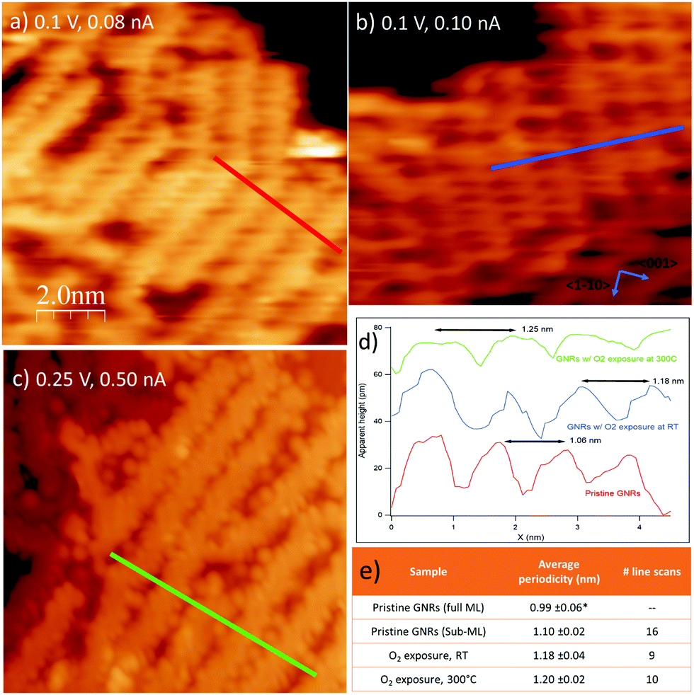 | ||
| Fig. 6 Close up images of the three preparations in Fig. 3 with corresponding line scans indicating the periodicity of the GNRs. (A) Pristine GNRs; (b) same as (a) after exposure to O2 at RT; (c) same as (a) after exposure to O2 at 300 °C. In this preparation the small features in-between the GNRs are evident. (d) Line scans cut along the paths marked in panels (a–c) showing that the separation between adjacent GNRs increases after O2 exposure. (e) Table summarizing the average separation between GNRs in ordered arrays, together with the number of line scans considered for each preparation (corresponding to the number of GNRs arrays considered). Values are given with their standard error. Data indicated with * are taken from ref. 12. | ||
Finally, we considered the small arrays of parallel GNRs, which are present for all the three preparations reported in Fig. 6 and we measured the separation between adjacent GNRs. Sample line scans drawn along the paths marked in panels (a–c) are reported in panel (d), while the table in panel (e) summarizes the outcome of a statistical analysis over several ordered arrays. The corresponding value measured for full monolayer coverage is also reported for comparison.12 Firstly, we note that, also for the sub-monolayer, GNRs tend to form arrays, though less densely packed than for the full monolayer coverage.12 The distance between adjacent nanostructures further increases upon oxygen exposure: the line scans present a less regular profile (the distance between maxima is not always the same, in accord with the more disordered distribution of the nanostructures) and, on average, the spacing between adjacent structures increases by ∼10% with respect to the pristine sample. We remark that this effect must be certainly ascribed to oxygen exposure; in fact, the samples in Fig. 3b, c and 6b, c were obtained by exposing the pristine sample of Fig. 3a and 6a, so that the initial density of GNRs is exactly the same. The larger separation between adjacent nanoribbons upon oxygen adsorption suggests that the O adatoms adsorbed on the first Ag layer or the O–Ag–O complexes act as “spacers”. It also indicates that, following oxygen exposure, the bonding of the nanostructure to the substrate gets weaker and the GNRs can displace along the surface without changing their geometry. This observation perfectly matches with the downshift of the main C 1s line observed in the corresponding XPS experiment (Fig. 5). The overall picture suggests therefore that the GNR-Ag interaction is weakened upon O2 exposure; in view of the observed C 1s core level shift, this effect is due more likely to oxygen intercalation than to modifications of the metal surface upon oxygen adsorption.
STS spectra would be extremely useful to determine if this weakening affects the width of the band-gap or its position with respect to the Fermi edge but, unfortunately, we were unable to record them with a useful signal-to-noise ratio due to the instability of the tip for samples exposed to oxygen. On the contrary, dI/dV maps could be acquired in the bias range −1.0 V < V < +1.0 V after dosing O2 at 300 °C.
Fig. 7 shows a comparison between such maps recorded near the band-gap edges for the pristine GNRs sample and for the same sample after exposure to O2 at 300 °C. We first observe a contrast change between positive (empty states) and negative (filled states) bias for the pristine GNRs. Indeed, at −250 mV the nanostructures appear narrower and the measured corrugation is larger than at +250 meV. This effect is much reduced after exposure to O2; in this case the images appear with a very similar contrast and the small differences at the edges are a consequence of the derivative operation. In addition, the nanostructures appear wider and their edges are much better defined than on the pristine surface. The effect goes well beyond the improved quality of the tip in this image. We recall that oxygen has intercalated under the GNRs and that some O adatoms must have reacted with the nanostructures, as witnessed by the presence of C 1s and O 1s components compatible with the formation of carbonyl groups in the XPS spectra. It is possible that these phenomena cause a better confinement of electrons within the GNR.
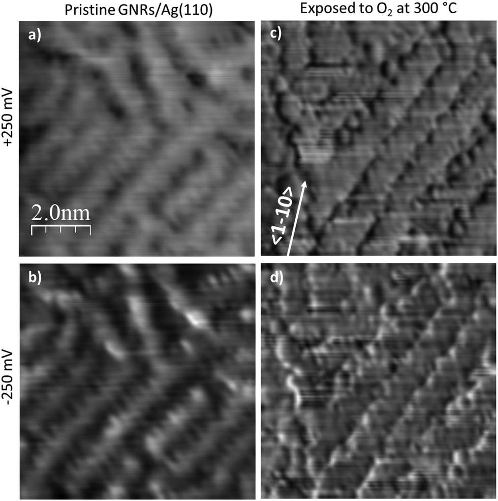 | ||
| Fig. 7 Comparison of the dI/dV maps of GNRs pristine and after exposure to oxygen at 300 °C. Bias voltages corresponding to the edges of the energy gap measured for the pristine sample are presented. The corresponding topographical images are those of Fig. 4a and 5c. Z-scale is the same for all images. | ||
Finally, we mention that previous literature on AGNRs reports that the nanostructures are affected by the presence of gases (water or oxygen) during the surface assisted synthesis30 but that, if grown under clean UHV conditions, their properties are stable even at atmospheric pressure.29 Our results are not in contradiction with these works since they refer to the morphology of the GNRs, which is also preserved in our case, while they did not perform any XPS analysis on the investigated systems.
Conclusion
Mixed edge-site, 1.0 nm wide GNRs grown on Ag(110) were characterized by LT-STM, STS and XPS and the effect of oxygen exposure in the 10−6 mbar range was addressed. An energy gap of ∼530 meV is measured for the pristine GNRs, in line with the values reported in literature, and two localized states, most probably related to quantum confinement, are found inside the gap.Upon oxygen exposure, the surface appears more disordered and the average separation between adjacent GNRs increases by ∼10%, while a downshift of the main C 1s peak is observed in the XPS spectrum. When O2 is dosed on the sample at T = 300 °C, a significant modification of the surface occurs, since Ag–O complexes appear on the surface both in-between the nanoribbons and at bare Ag patches. The overall appearance of the GNRs in morphological images does not change significantly, but the formation of carboxyl groups is detected by photoemission spectroscopy, suggesting that some C atoms of the GNRs have reacted with oxygen adatoms. Coherently, dI/dV maps recorded on the pristine and oxygen-exposed samples are different, suggesting that oxygen must play an active role. Its adsorption reduces the interaction between the nanostructures and the Ag(110) substrate and thus favours their displacement and electronic decoupling.
These results clearly demonstrate that care must be taken about the modification of supported GNRs upon exposure to reactive gases, not only for their possible interaction with the nanostructures, but also for the changes induced by the reactant on the whole system. This insight opens important perspectives for the optimization of the transfer procedure of the nanoribbons on a different substrate, as well as for operating nanostructure-based devices under realistic conditions.
Conflicts of interest
There are no conflicts to declare.Acknowledgements
We thank Angelique J. Lusuan and Jade Chalancon for taking part to the initial stages of the experiment and to acquisition of STS spectra, respectively. We acknowledge financial support from MIUR through projects PRIN2017 project no. 2017NYPHN8 and FIRB Futuro in Ricerca 2012 No. RBFR128BEC. L. S., M. S., L. V. and M. R. acknowledge funding from Fondazione Compagnia di S. Paolo through project MC-nano. I. P., E. M., S. N. and F. B. acknowledge funding from EUROFEL project (RoadMap Esfri). We acknowledge Elettra Sincrotrone Trieste for providing access to its synchrotron radiation facilities. P. W. acknowledges financial support from the European Social Fund through the Operational Programme Knowledge Education Development project “Interdisciplinary PhD studies in nanotechnology” (project no. POWR.03.02.00-00-I032/16) and, partially, from the National Science Centre of Poland through the OPUS project no. 2014/15/B/ST3/02927.References
- X. Li, X. Wang, L. Zhang, S. Lee and H. Dai, Chemically derived, ultrasmooth graphene nanoribbon semiconductors, Science, 2008, 319, 1229–1232 CrossRef CAS.
- K. Nakada, M. Fujita, G. Dresselhaus and M. S. Dresselhaus, Edge state in graphene ribbons: nanometer size effect and edge shape dependence, Phys. Rev. B: Condens. Matter Mater. Phys., 1996, 54, 17954–17961 CrossRef CAS.
- Y.-C. Chen, D. G. de Oteyza, Z. Pedramrazi, C. Chen, F. R. Fischer and M. F. Crommie, Tuning the band gap of graphene nanoribbons synthesized from molecular precursors, ACS Nano, 2013, 7, 6123–6128 CrossRef CAS.
- X. Wang, Y. Ouyang, X. Li, H. Wang, J. Guo and H. Dai, Room-temperature all-semiconducting sub-10-nm graphene nanoribbon field-effect transistors, Phys. Rev. Lett., 2008, 100, 206803 CrossRef.
- J. Baringhaus, M. Ruan, F. Edler, A. Tejeda, M. Sicot, A. Taleb-Ibrahimi, A.-P. Li, Z. Jiang, E. H. Conrad, C. Berger, C. Tegenkamp and W. A. de Heer, Exceptional ballistic transport in epitaxial graphene nanoribbons, Nature, 2014, 506, 349–354 CrossRef CAS.
- M. Y. Han, B. Özyilmaz, Y. Zhang and P. Kim, Energy band-gap engineering of graphene nanoribbons, Phys. Rev. Lett., 2007, 98, 206805 CrossRef.
- L. Jiao, L. Zhang, X. Wang, G. Diankov and H. Dai, Narrow graphene nanoribbons from carbon nanotubes, Nature, 2009, 458, 877–880 CrossRef CAS.
- D. V. Kosynkin, A. L. Higginbotham, A. Sinitskii, J. R. Lomeda, A. Dimiev, B. K. Price and J. M. Tour, Longitudinal unzipping of carbon nanotubes to form graphene nanoribbons, Nature, 2009, 458, 872–876 CrossRef CAS.
- X. Yang, X. Dou, A. Rouhanipour, L. Zhi, H. J. Räder and K. Müllen, Two-dimensional graphene nanoribbons, J. Am. Chem. Soc., 2008, 130, 4216–4217 CrossRef CAS.
- P. Han, K. Akagi, F. Federici Canova, H. Mutoh, S. Shiraki, K. Iwaya, P. S. Weiss, N. Asao and T. Hitosugi, Bottom-up graphene-nanoribbon fabrication reveals chiral edges and enantioselectivity, ACS Nano, 2014, 8, 9181–9187 CrossRef CAS.
- J. Cai, P. Ruffieux, R. Jaafar, M. Bieri, T. Braun, S. Blankenburg, M. Muoth, A. P. Seitsonen, M. Saleh, X. Feng, K. Müllen and R. Fasel, Atomically precise bottom-up fabrication of graphene nanoribbons, Nature, 2010, 466, 470–473 CrossRef CAS.
- M. Smerieri, I. Pis, L. Ferrighi, S. Nappini, A. J. Lusuan, C. di Valentin, L. Vaghi, A. Papagni, M. Cattelan, S. Agnoli, E. Magnano, F. Bondino and L. Savio, Synthesis of graphene nanoribbons with a defined mixed edge-site sequence by surface assisted polymerization of (1,6)-dibromopyrene on Ag(110), Nanoscale, 2016, 8, 17843–17853 RSC.
- G. Franc and A. Gourdon, Covalent networks through on-surface chemistry in ultra-high vacuum: State-of-the-art and recent developments, Phys. Chem. Chem. Phys., 2011, 13, 14283–14292 RSC.
- S.-W. Hla, L. Bartels, G. Meyer and K.-H. Rieder, Inducing all steps of a chemical reaction with the scanning tunneling microscope tip: towards single molecule engineering, Phys. Rev. Lett., 2000, 85, 2777–2780 CrossRef CAS.
- A. Lafferentz, M. Wenderoth, S. Lounis, P. Zahn, N. Quaas, R. G. Ulbrich, P. H. Dederichs and S. Blugel, Conductance of a single conjugated polymer as a continuous function of its length, Science, 2009, 323, 1190–1193 CrossRef.
- X. Zhou and G. Yu, Modified engineering of graphene nanoribbons prepared via on-surface synthesis, Adv. Mater., 2020, 32, 1–24 CAS.
- J. Liu, B. W. Li, Y. Z. Tan, A. Giannakopoulos, C. Sanchez-Sanchez, D. Beljonne, P. Ruffieux, R. Fasel, X. Feng and K. Müllen, Toward cove-edged low band gap graphene nanoribbons, J. Am. Chem. Soc., 2015, 137, 6097–6103 CrossRef CAS.
- Q. Fan, J. M. Gottfried and J. Zhu, Surface-catalyzed C–C covalent coupling strategies toward the synthesis of low-dimensional carbon-based nanostructures, Acc. Chem. Res., 2015, 48, 2484–2494 CrossRef CAS.
- P. Ruffieux, S. Wang, B. Yang, C. Sanchez-Sanchez, J. Liu, T. Dienel, L. Talirz, P. Shinde, C. A. Pignedoli, D. Passerone, T. Dumslaff, X. Feng, K. Müllen and R. Fasel, On-surface synthesis of graphene nanoribbons with zigzag edge topology, Nature, 2016, 531, 489–492 CrossRef CAS.
- K. A. Simonov, N. A. Vinogradov, A. S. Vinogradov, A. V. Generalov, E. M. Zagrebina, N. Mårtensson, A. A. Cafolla, T. Carpy, J. P. Cunniffe and A. B. Preobrajenski, Effect of substrate chemistry on the bottom-up fabrication of graphene nanoribbons: combined core-level spectroscopy and STM study, J. Phys. Chem. C, 2014, 118, 12532–12540 CrossRef CAS.
- K. A. Simonov, N. A. Vinogradov, A. S. Vinogradov, A. V. Generalov, E. M. Zagrebina, G. I. Svirskiy, A. A. Cafolla, T. Carpy, J. P. Cunniffe, T. Taketsugu, A. Lyalin, N. Mårtensson and A. B. Preobrajenski, From graphene nanoribbons on Cu(111) to nanographene on Cu(110): critical role of substrate structure in the bottom-up fabrication strategy, ACS Nano, 2015, 9, 8997–9011 CrossRef CAS.
- Y. Li, W. Zhang, M. Morgenstern and R. Mazzarello, Electronic and magnetic properties of zigzag graphene nanoribbons on the (111) surface of Cu, Ag, and Au, Phys. Rev. Lett., 2013, 110, 1–5 Search PubMed.
- L. Yan and P. Liljeroth, Engineered electronic states in atomically precise artificial lattices and graphene nanoribbons, Adv. Phys. X, 2019, 4, 1651672 CAS.
- M. Smerieri, I. Píš, L. Ferrighi, S. Nappini, A. Lusuan, L. Vattuone, L. Vaghi, A. Papagni, E. Magnano, C. Di Valentin, F. Bondino and L. Savio, Synthesis of corrugated C-based nanostructures by Br-corannulene oligomerization, Phys. Chem. Chem. Phys., 2018, 20, 26161–26172 RSC.
- I. Píš, L. Ferrighi, T. H. Nguyen, S. Nappini, L. Vaghi, A. Basagni, E. Magnano, A. Papagni, F. Sedona, C. Di Valentin, S. Agnoli and F. Bondino, Surface-confined polymerization of halogenated polyacenes: the case of dibromotetracene on Ag(110), J. Phys. Chem. C, 2016, 120, 4909–4918 CrossRef.
- A. Kimouche, M. M. Ervasti, R. Drost, S. Halonen, A. Harju, P. M. Joensuu, J. Sainio and P. Liljeroth, Ultra-narrow metallic armchair graphene nanoribbons, Nat. Commun., 2015, 6, 10177 CrossRef CAS.
- J. Cai, C. A. Pignedoli, L. Talirz, P. Ruffieux, H. Söde, L. Liang, V. Meunier, R. Berger, R. Li, X. Feng, K. Müllen and R. Fasel, Graphene nanoribbon heterojunctions, Nat. Nanotechnol., 2014, 9, 896–900 CrossRef CAS.
- S. Kawai, S. Saito, S. Osumi, S. Yamaguchi, A. S. Foster, P. Spijker and E. Meyer, Atomically controlled substitutional boron-doping of graphene nanoribbons, Nat. Commun., 2015, 6, 8098 CrossRef CAS.
- G. Borin Barin, A. Fairbrother, L. Rotach, M. Bayle, M. Paillet, L. Liang, V. Meunier, R. Hauert, T. Dumslaff, A. Narita, K. Müllen, H. Sahabudeen, R. Berger, X. Feng, R. Fasel and P. Ruffieux, Surface-synthesized graphene nanoribbons for room temperature switching devices: substrate transfer and ex situ characterization, ACS Appl. Nano Mater., 2019, 2, 2184–2192 CrossRef CAS.
- A. Fairbrother, J. R. Sanchez-Valencia, B. Lauber, I. Shorubalko, P. Ruffieux, T. Hintermann and R. Fasel, High vacuum synthesis and ambient stability of bottom-up graphene nanoribbons, Nanoscale, 2017, 9, 2785–2792 RSC.
- T. B. Rawal, M. Smerieri, J. Pal, S. Hong, M. Alatalo, L. Savio, L. Vattuone, T. S. Rahman and M. Rocca, Deciphering complex features in STM images of O adatoms on Ag(110), Phys. Rev. B, 2018, 98, 35405 CrossRef CAS.
- L. Savio, M. Smerieri, L. Vattuone, A. Gussoni, C. Tassistro and M. Rocca, STM study of hydroxyl formation at O/Ag(110), Phys. Rev. B: Condens. Matter Mater. Phys., 2006, 74, 1–6 CrossRef.
- I. Horcas, R. Fernandez, J. Gomez-Rodriguez, J. Colchero, J. Gomez-Herrero and A. Baro, Rev. Sci. Instrum., 2007, 78, 013705 CrossRef CAS.
- S. Doniach and M. Sunjic, Many-electron singularity in X-ray photoemission and X-ray line spectra from metals, J. Phys. C: Solid State Phys., 1970, 3, 285–291 CrossRef CAS.
- J. J. Joyce, M. Del Giudice and J. H. Weaver, Quantitative analysis of synchrotron radiation photoemission core level data, J. Electron Spectrosc. Relat. Phenom., 1989, 49, 31–45 CrossRef CAS.
- F. C. Henn, M. E. Bussell and C. T. Campbell, A simple means for reproducibly dosing low vapor pressure and/or reactive gases to surfaces in ultrahigh vacuum, J. Vac. Sci. Technol., A, 1991, 9, 10–13 CrossRef CAS.
- C. Moreno, M. Panighel, M. Vilas-Varela, G. Sauthier, M. Tenorio, G. Ceballos, D. Peña and A. Mugarza, Critical role of phenyl substitution and catalytic substrate in the surface-assisted polymerization of dibromobianthracene derivatives, Chem. Mater., 2019, 31, 331–341 CrossRef CAS.
- J. Hu, J. Hu, Z. Zhang, K. Shen, Z. Liang, H. Zhang, Q. Tian, P. Wang, Z. Jiang, H. Huang, J. W. Wells and F. Song, Ullmann coupling of 2,7-dibromopyrene on Au(111) assisted by surface adatoms, Appl. Surf. Sci., 2020, 513, 145797 CrossRef CAS.
- A. Basagni, F. Sedona, C. A. Pignedoli, M. Cattelan, L. Nicolas, M. Casarin and M. Sambi, Molecules–oligomers–nanowires–graphene nanoribbons: a bottom-up stepwise on-surface covalent synthesis preserving long-range order, J. Am. Chem. Soc., 2015, 137, 1802–1808 CrossRef CAS.
- A. Mairena, M. Baljozovic, M. Kawecki, K. Grenader, M. Wienke, K. Martin, L. Bernard, N. Avarvari, A. Terfort, K.-H. Ernst and C. Wäckerlin, The fate of bromine after temperature-induced dehydrogenation of on-surface synthesized bisheptahelicene, Chem. Sci., 2019, 10, 2998–3004 RSC.
- G. Giovannetti, P. A. Khomyakov, G. Brocks, V. M. Karpan, J. Van Den Brink and P. J. Kelly, Doping graphene with metal contacts, Phys. Rev. Lett., 2008, 101, 3–6 Search PubMed.
- A. Dahal and M. Batzill, Graphene–nickel interfaces: a review, Nanoscale, 2014, 6, 2548–2562 RSC.
- L. G. Bulusheva, V. E. Arkhipov, K. M. Popov, V. I. Sysoev, A. A. Makarova and A. V. Okotrub, Electronic structure of nitrogen-and phosphorus-doped graphenes grown by chemical vapor deposition method, Materials, 2020, 13, 1173 CrossRef CAS.
- R. Wu, J. Ren, L. Dong, Y. Wang, Q. Huan and H. J. Gao, Quasi-free-standing graphene nano-islands on Ag(110), grown from solid carbon source, Appl. Phys. Lett., 2017, 110, 213107 CrossRef.
- C. Riedl, C. Coletti, T. Iwasaki, A. A. Zakharov and U. Starke, Quasi-free-standing epitaxial graphene on SiC obtained by hydrogen intercalation, Phys. Rev. Lett., 2009, 103, 2–5 CrossRef.
- S. L. Kovalenko, B. V. Andryushechkin and K. N. Eltsov, STM study of oxygen intercalation at the graphene/Ni(111) interface, Carbon, 2020, 164, 198–206 CrossRef CAS.
- R. Larciprete, S. Ulstrup, P. Lacovig, M. Dalmiglio, M. Bianchi, F. Mazzola, L. Hornekær, F. Orlando, A. Baraldi, P. Hofmann and S. Lizzit, Oxygen switching of the epitaxial graphene–metal interaction, ACS Nano, 2012, 6, 9551–9558 CrossRef CAS.
- R. Blume, P. R. Kidambi, B. C. Bayer, R. S. Weatherup, Z. J. Wang, G. Weinberg, M. G. Willinger, M. Greiner, S. Hofmann, A. Knop-Gericke and R. Schlögl, The influence of intercalated oxygen on the properties of graphene on polycrystalline Cu under various environmental conditions, Phys. Chem. Chem. Phys., 2014, 16, 25989–26003 RSC.
- P. Sutter, P. Albrecht, X. Tong and E. Sutter, Mechanical decoupling of graphene from Ru(0001) by interfacial reaction with oxygen, J. Phys. Chem. C, 2013, 117, 6320–6324 CrossRef CAS.
- L. Vattuone, M. Rocca, C. Boragno and U. Valbusa, Initial sticking coefficient of O2 on Ag(110), J. Chem. Phys., 1994, 101, 713–725 CrossRef CAS.
- Y. C. G. Kwan, G. M. Ng and C. H. A. Huan, Identification of functional groups and determination of carboxyl formation temperature in graphene oxide using the XPS O 1s spectrum, Thin Solid Films, 2015, 590, 40–48 CrossRef CAS.
- A. Ganguly, S. Sharma, P. Papakonstantinou and J. Hamilton, Probing the thermal deoxygenation of graphene oxide using high-resolution in situ X-ray-based spectroscopies, J. Phys. Chem. C, 2011, 115, 17009–17019 CrossRef CAS.
- U. Zielke, K. J. Hüttinger and W. P. Hoffman, Surface-oxidized carbon fibers: I. Surface structure and chemistry, Carbon, 1996, 34, 983–998 CrossRef CAS.
- J. Matthew, Surface analysis by Auger and X-ray photoelectron spectroscopy. D. Briggs and J. T. Grant (eds). IMPublications, Chichester, UK and SurfaceSpectra, Manchester, UK, 2003. 900 pp., ISBN 1-901019-04-7, 900 pp, Surf. Interface Anal., 2004, 36, 1647 CrossRef CAS.
| This journal is © the Owner Societies 2021 |