First-principles calculations of phonon behaviors in graphether: a comparative study with graphene†
Received
14th June 2020
, Accepted 23rd September 2020
First published on 23rd September 2020
Abstract
Recently, a two-dimensional (2D) oxocarbon monolayer, graphether, has been arousing extensive attention owing to its excellent electrical properties. In this work, we calculate the lattice thermal conductivity (k) of graphether and graphene using first-principles calculations and the phonon Boltzmann transport equation. At 300 K, the lattice thermal conductivities of graphether and graphene along the armchair direction are 600.91 W m−1 K−1 and 3544.41 W m−1 K−1, respectively. Moreover, the electron localization function is employed to reveal the origin of the anisotropic k of graphether. Furthermore, the harmonic and anharmonic properties of graphether and graphene are analyzed. We attribute the lower k of graphether to the smaller phonon group velocity and shorter phonon lifetime. Finally, the size effects of phonon transport in graphether and graphene are studied, and the results show that the lattice thermal conductivities are significantly dependent on the system length. The analysis of phonon behaviors in our study contributes to an in-depth understanding of the thermal transport in graphether for the first time, which provides valuable guidelines for graphether-based phonon engineering applications and 2D nanoelectronic devices.
1. Introduction
Graphene is a pioneering two-dimensional (2D) material that is a monolayer of carbon atoms assembled in a regular honeycomb lattice.1 Graphene has attracted considerable attention in both fundamental research studies and practical applications due to its ultrahigh thermal conductivity, outstanding electrical mobility, excellent mechanical strength and optical transmittance.2–5 Mechanical exfoliation, liquid-phase exfoliation, thermal exfoliation, and chemical vapor deposition are widely used in the production of graphene.1,6–8 However, the features of a zero band gap and extremely low on/off ratio in graphene hinder its application in nanoelectronic devices, such as field effect transistors.9 Therefore, it is crucial to explore new 2D materials with a tunable band gap and desired physical properties.
Previous studies have confirmed that the physical properties of graphene can be tuned by adding doping atoms and chemical functionalization, such as C2N, C3N, and hydrogenated graphene.10–15 Recently, a new 2D oxocarbon monolayer, graphether, has been theoretically designed by bottom-up fabrication via the on-surface assembly of dimethyl ether molecules.16 Graphether had an excellent thermodynamic stability, a direct band gap of 2.39 eV, and strong light absorption in the ultraviolet region.16 Moreover, the direct band gap could still be maintained under uniaxial or biaxial strain from −10% to 10%. On account of the hyperconjugative interaction, the in-plane (x–y) stiffness of graphether along the armchair direction (∼459.8 N m−1) exceeded that of graphene (∼342 N m−1). Furthermore, the carrier mobilities of graphether reached 1.8 × 103 cm2 V−1 s−1 and 1.7 × 103 cm2 V−1 s−1 along the armchair and zigzag directions, separately, which were larger than those of hydrogenated and fluorinated graphene (45–105 cm2 V−1 s−1).16,17 Therefore, we can deduce that graphether can be used as a candidate for a new generation nanoelectronic material owing to these excellent physical properties.
In practice, if devices cannot efficiently dissipate heat, the excess heat can lead to device performance degradation, defect formation, and material invalidation. Regarding obtaining outstanding electrical performance and a long lifetime, the thermal properties of materials play a crucial role in the thermal management within nanoelectronic devices. It has been reported that the thermal conductivity of graphene was 3716.60 W m−1 K−1.18 Many studies have demonstrated that graphene can be used to improve the heat dissipation ability of 2D semiconductor based nanoelectronic devices.11,19 In view of the fact that electronic devices extremely rely on the thermal properties, investigation of the thermal conductivity in graphether is necessary. Nevertheless, to the best of our knowledge, there are no experimental or theoretical studies on the thermal properties of graphether. Therefore, the lattice thermal conductivity (k) and phonon behaviors of graphether are evaluated for the first time in this paper, which provides guidelines for designing graphether-based nanoelectronic devices and fills a blank in the phonon behavior analysis of the 2D oxocarbon materials field.
In this work, we systematically investigate k of graphether by using first-principles calculations combined with the phonon Boltzmann transport equation (BTE) and compute k of graphene as a comparative study. First, we obtain optimized structures and calculate k of graphether and graphene. The electron localization function (ELF) is applied to further explain the anisotropic k of graphether. Moreover, phonon dispersion curves and phonon group velocities of graphether and graphene are applied to interpret phonon behaviors. The Grüneisen parameter and phase space are studied to describe the anharmonic properties. Furthermore, we also evaluate the phonon lifetimes and phonon mean free paths (MFPs) of graphether and graphene. Finally, the effects of system size on the lattice thermal conductivities of graphether and graphene are explored by considering the phonon-boundary scattering rate. Our work sheds light on the thermal transport properties of graphether, which is beneficial to the thermal management of nanoelectronic devices.
2. Methodology
All first-principles calculations are performed by using density functional theory (DFT)20,21 as implemented in the Vienna ab initio simulation package (VASP).22,23 The generalized gradient approximation (GGA)24 with Perder–Burke–Ernzerhof (PBE) for the exchange–correlation energy is employed. A plane-wave set is utilized with a kinetic energy cutoff of 600 eV. For the geometry optimization and ELF calculations, the k meshes in the Brillouin zone are set to 13 × 18 × 1 and 21 × 21 × 1 for graphether and graphene, respectively. Geometry structures are fully optimized until the force convergence criterion is less than 10−4 eV Å−1 and energy convergence criterion is less than 10−6 eV. The vacuum thickness is larger than 15 Å along the z direction to prevent the atomic interaction with the image of the system. We utilize the Visualization for Electronic and Structural Analysis (VESTA)25 package for the illustration of atomic structures and ELF.
The lattice thermal conductivity can be calculated as a sum of the contribution of all phonon modes:26
| | 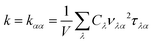 | (1) |
where
V is the volume of a unit cell,
Cλ denotes the heat capacity per mode, and
vλα and
τλα represent the phonon group velocity and phonon lifetime of mode
λ along the
α direction, respectively.
27k can be calculated iteratively by using ShengBTE code based on the BTE,
28–30 which is widely used in many 2D materials.
18,31 Phonon properties are mainly determined by interatomic force constants (IFCs). ShengBTE requires two main input files,
i.e., second-order (harmonic) and third-order (anharmonic) IFCs, which are obtained from first-principles calculations. Using the second-order IFCs, we estimate phonon dispersion curves of graphether and graphene, which determine the heat capacity and phonon group velocity. The third-order IFCs play an important role in calculating the three-phonon scattering rate, which is the inverse of phonon lifetime.
We use Phonony32 to compute second-order IFCs by using density functional perturbation theory (DFPT).21 A 3 × 3 × 1 supercell with a 5 × 6 × 1 q mesh is utilized for graphether. Similarly, for graphene, a 5 × 5 × 1 supercell with a 5 × 5 × 1 q mesh is applied. The thirdorder.py script file is used to generate a minimal set of displaced supercell configurations. The same supercell and q mesh are employed to obtain the third-order IFCs. The Born effective charges and dielectric tensor33 are considered to interpret long-range electrostatic interactions in polar compounds, which added a long-range correction to the dynamical matrix.34,35 To ensure the convergence of k, the q point grids for graphether and graphene are set to 30 × 42 × 1 and 100 × 100 × 1, respectively. The layer thicknesses are 5.65 Å and 3.40 Å for graphether and graphene to obtain the lattice thermal conductivity.16,18
3. Results and discussion
3.1 Optimized structure, lattice thermal conductivity, and electron localization function
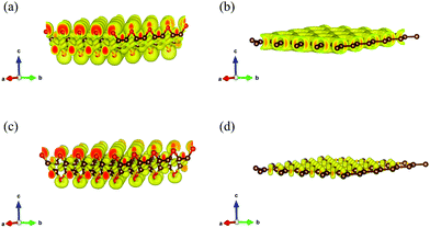
The optimized structures of graphether and graphene are plotted in Fig. 1, both of which have armchair (along the x direction) and zigzag (along the y direction) directions. The unit cell of graphether consists of four carbon (C) atoms and two oxygen (O) atoms with optimized lattice parameters (a = 3.62 Å, b = 2.58 Å) and buckling distance (dz = 2.84 Å). Our results agree well with the previous work (a = 3.61 Å, b = 2.58 Å and dz = 2.85 Å).16 The unit cell of graphene includes two C atoms with the optimized lattice parameter of a = 2.47 Å, which is the same as that of a previous theoretical calculation (a = 2.47 Å).18 As shown in Fig. 1, there are two types of C–C bonds in graphether, in which the bond lengths are 1.60 Å and 1.53 Å, respectively. The lengths of the C–O bond in graphether and the C–C bond in graphene are both 1.43 Å.
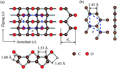 |
| | Fig. 1 Schematic diagrams of the optimized structures of graphether and graphene. (a) Top and side views of graphether. (b) Top and side views of graphene. The dashed lines represent the unit cells of graphether and graphene. The brown and red spheres represent C atoms and O atoms, respectively. | |
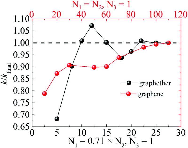
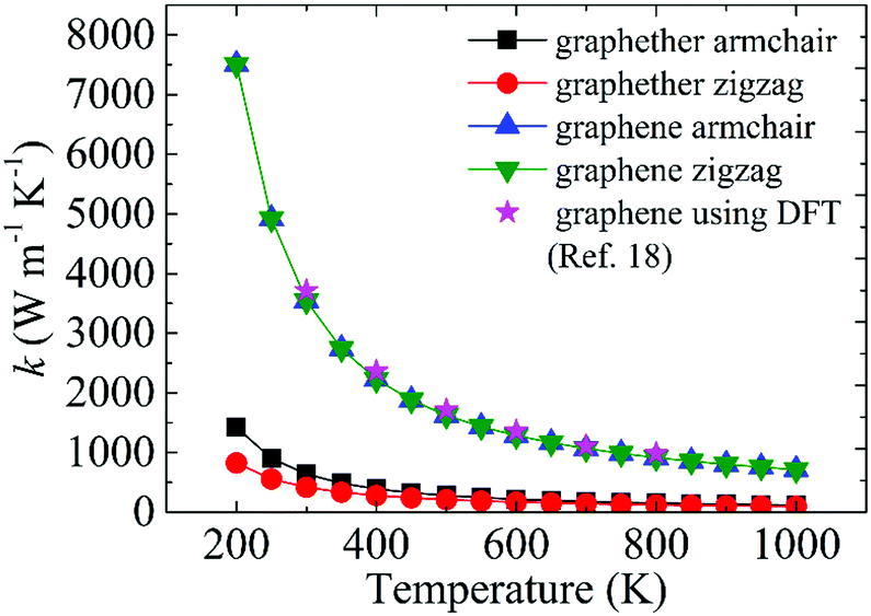
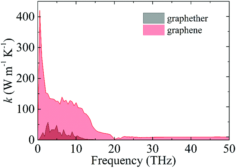
Moreover, we perform the convergence test of k at different numbers of q points along each axis, as shown in Fig. 2. It is observed that as the number of grids increases, the lattice thermal conductivities of graphether and graphene increase firstly and then stabilize generally. Therefore, the grids of 30 × 42 × 1 and 100 × 100 × 1 for graphether and graphene are chosen to increase the accuracy of the subsequent lattice thermal conductivity calculation. The lattice thermal conductivities of graphether and graphene along the armchair and zigzag directions as a function of temperature are plotted in Fig. 3. On one hand, we observe that the lattice thermal conductivities of graphene are isotropic and they are 3544.41 W m−1 K−1 along the armchair and zigzag directions at 300 K, which is comparable with the previous study (3716.60 W m−1 K−1).18 However, the lattice thermal conductivities of graphether are anisotropic, being 600.91 W m−1 K−1 and 393.32 W m−1 K−1 along the armchair and zigzag directions, respectively. k of graphether is much lower than that of graphene, which will be further discussed in the following section. Although k of graphether is lower than that of graphene, it is still larger than those of many representative 2D monolayer materials. The thermal conductivities of representative 2D monolayers calculated with first-principles calculations are listed in Table S1 in the ESI.† On the other hand, as the temperature increases from 200 to 1000 K, the lattice thermal conductivities of graphether and graphene decrease monotonically, and the corresponding reduction ratios are 91.65% and 90.47%, respectively. This phenomenon can be attributed to the more activated high frequency phonons, which results in the stronger phonon–phonon scattering.36–38 Similar trends are widespread in other 2D materials, such as phosphorene, WS2, and MoS2.31,39–41 To reveal the contribution of different frequency phonons to the total lattice thermal conductivity, we computed the frequency-dependent k of graphether and graphene at 300 K (Fig. 4). It can be observed that the low frequency phonon modes play dominant roles in k whereas high frequency phonon modes contribute little to k, which is consistent with the results of previous study.18
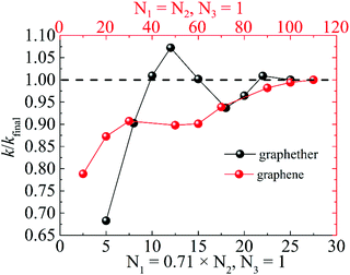 |
| | Fig. 2 The ratio of lattice thermal conductivity to final lattice thermal conductivity (k/kfinal) for graphether and graphene at different numbers of q points along each axis. | |
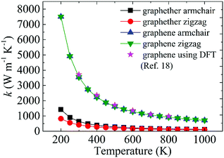 |
| | Fig. 3 The thermal conductivity variations of graphether and graphene at different temperatures from 200 to 1000 K. The magenta legend represents the DFT results of graphene taken from ref. 18. | |
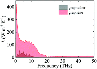 |
| | Fig. 4 The contribution of different frequency phonons to the total lattice thermal conductivities of graphether and graphene at 300 K. | |
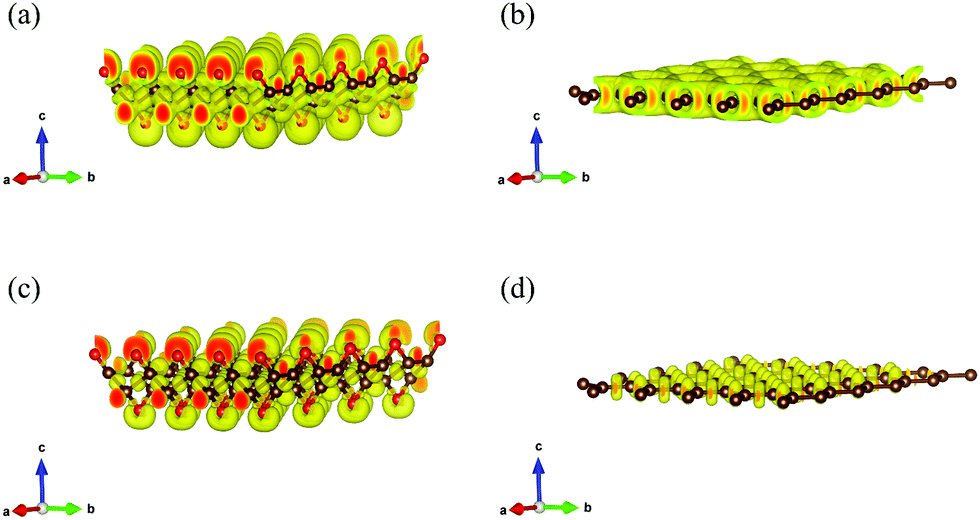
To further explore the fundamental difference in bond anharmonicity, we evaluate the ELF of graphether and graphene. It is an empirical three-dimensional (3D) function that considers the excess local kinetic energy generated by Pauli repulsion to characterize the chemical bonds.42 As a pure ground-state property, ELF is an effective channel to differentiate the nature of different types of bonds with a range from 0 to 1, where 0 represents no electrons, 0.5 corresponds to electron-gas-like pair probably, and 1 means highly localized and bound electrons.12,43Fig. 5 displays the 3D characteristic of the ELFs of graphether and graphene with unit cells of 4 × 4 × 1. Two phenomena can be observed as follows: (1) for graphether, the maximum ELF value locates at O atoms and small values locate at C atoms, which reflects a charge transfer interaction from C atoms to O atoms. For graphene, the C–C bond is a pure single σ-bond, which is formed by the head-to-head merging of sp2 hybridized orbitals from two C atoms. This bond is featured by highly localized electrons between the two C atoms. (2) By changing the isosurface value of ELF between 0.5 and 1.0, the electron localization can be resolved by the contours into some domains, which are named bonding attractors.43 As shown in Fig. 5(a and b), an ELF value of 0.60 gives a continuous isosurface,44 which describes a region of electron localization. When the value of ELF is equal to 0.80 (Fig. 5(c and d)),43 the isosurface separates into a local maximum. For graphether, the distribution of bonding attractors accords with the polarized covalent C–O bond by virtue of the electronegativity difference between O (3.44) and C (2.55).45 The O atoms are in the red region with higher ELF values, which displays the polarized bond character of covalent C–O bonds. The covalent character is depicted in the oval shaped ELF of the C atom directed toward the O atom. For the O atom, an ELF value of 0.80 also contributes a banana-shaped lone pair character over the apex of the C–O–C bond, which is perpendicular to the C–O–C plane. However, graphene displays a uniform charge density distribution because of most electrons gathering between C–C bonds. Therefore, we can conclude that the non-planar structure of graphether leads to the anisotropic properties, which include the anisotropic k along the armchair and zigzag directions. In order to accurately correct the electronic structure of graphether, the hybrid density functional by Heyd–Scuseria–Ernzerhof (HES06) is adopted.46 The band gaps of graphether are 0.74 eV for the PBE and 2.41 eV for the HSE06 hybrid functionals, which are given in Fig. S1 of the ESI.†
 |
| | Fig. 5 The 3D isosurfaces describing the electron localization function (ELF). The red spheres represent oxygen atoms, the brown spheres represent the neighboring carbon atoms. (a) Graphether, ELF = 0.60, (b) graphene, ELF = 0.60, (c) graphether, ELF = 0.80 and (d) graphene, ELF = 0.80. | |
3.2 Phonon dispersion curve and phonon group velocity
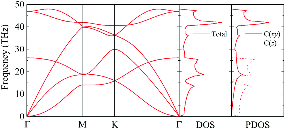
The phonon dispersion curve and phonon group velocity are widely used to reveal the underlying phonon behavior information. We evaluate the phonon dispersion curves, the phonon density of states (DOS), and the partial density of states (PDOS) of graphether and graphene, as shown in Fig. 6 and 7, which are consistent with experimental and theoretical works.16,47–49 There are six atoms in a graphether unit cell, which causes three acoustic phonon modes and fifteen optical phonon modes. For graphene, there are two atoms in a unit cell, which leads to three acoustic phonon modes and three optical phonon modes. It can be found that there are no imaginary frequencies in graphether and graphene, which indicates that both structures are thermodynamically stable. Furthermore, the calculated cohesive energy and total energy of graphether are higher than those of some 2D materials, as shown in Fig. S2 and S3 in the ESI,† which can also prove its stability. According to elastic theory, the flexural acoustic (ZA) phonon mode should possess a quadratic dispersion with an unstressed sheet.18,50 As depicted in Fig. 6 and 7, ZA phonon modes of both graphether and graphene show quadratic curves near the Γ high symmetry point. However, the transverse acoustic (TA) and longitudinal acoustic (LA) phonon modes of graphether and graphene are linear around the Γ point. It is obvious that the frequency range of graphether is narrower than that of graphene. The highest frequency of the optical phonon modes of graphether can reach up to 40.75 THz, which is higher than those of black phosphorene (∼13.5 THz)51 and MoS2 (∼15 THz).52 This phenomenon demonstrates the robustness of covalent C–O and C–C interactions in graphether. To analyze the effect of different atoms on k, we further calculate the DOS and PDOS of graphether and graphene, which are depicted in Fig. 6 and 7, respectively. For graphether (Fig. 6), the C atom vibrates in the full frequency range and the O atom vibrates in the range of 0–38.92 THz. The C atom has an important contribution in all phonon modes, whereas the O atom mainly plays a role in the low frequency region and the intermediate frequency region. In the high frequency region (more than 35 THz), the contribution of the O atom to the DOS is negligible because of the different relative atomic masses. The high frequency vibration is mainly provided by the lighter atoms (C), while the heavy atoms (O) occupy a dominant position in the low frequency vibration, which is similar to BeO and B4H4 monolayers.53,54 For graphene (Fig. 7), the smooth optical phonon modes will generate some peaks of DOS in the range of 40–50 THz due to the transition of the C![[double bond, length as m-dash]](https://www.rsc.org/images/entities/char_e001.gif) C double bond to the C–C single bond.55 At the Γ point, the phonon mode mainly vibrates in the z direction. It should be noted that the in-plane phonon modes (TA, LA, TO, and LO) of graphene are completely decoupled with the out-of-plane phonon modes (ZA and ZO). However, the covalent bonds of graphether become nonorthogonal both in-plane and out-of-plane due to the non-planar structure, which results in hybridization between the in-plane and out-of-plane vibrations. Moreover, it has been demonstrated that non-planar structures usually lead to a lower k because of the disruption of the out-of-plane symmetry.56 Therefore, doping O atoms in graphene converts the planar structure to a non-planar structure, resulting in a lower k of graphether, which can be attributed to the lower phonon group velocity and phonon lifetime (as discussed in more detail in the following sections).
C double bond to the C–C single bond.55 At the Γ point, the phonon mode mainly vibrates in the z direction. It should be noted that the in-plane phonon modes (TA, LA, TO, and LO) of graphene are completely decoupled with the out-of-plane phonon modes (ZA and ZO). However, the covalent bonds of graphether become nonorthogonal both in-plane and out-of-plane due to the non-planar structure, which results in hybridization between the in-plane and out-of-plane vibrations. Moreover, it has been demonstrated that non-planar structures usually lead to a lower k because of the disruption of the out-of-plane symmetry.56 Therefore, doping O atoms in graphene converts the planar structure to a non-planar structure, resulting in a lower k of graphether, which can be attributed to the lower phonon group velocity and phonon lifetime (as discussed in more detail in the following sections).
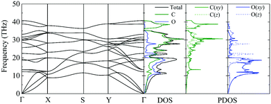 |
| | Fig. 6 The phonon dispersion curve, DOS, and PDOS of graphether. | |
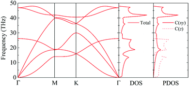 |
| | Fig. 7 The phonon dispersion curve, DOS, and PDOS of graphene. | |
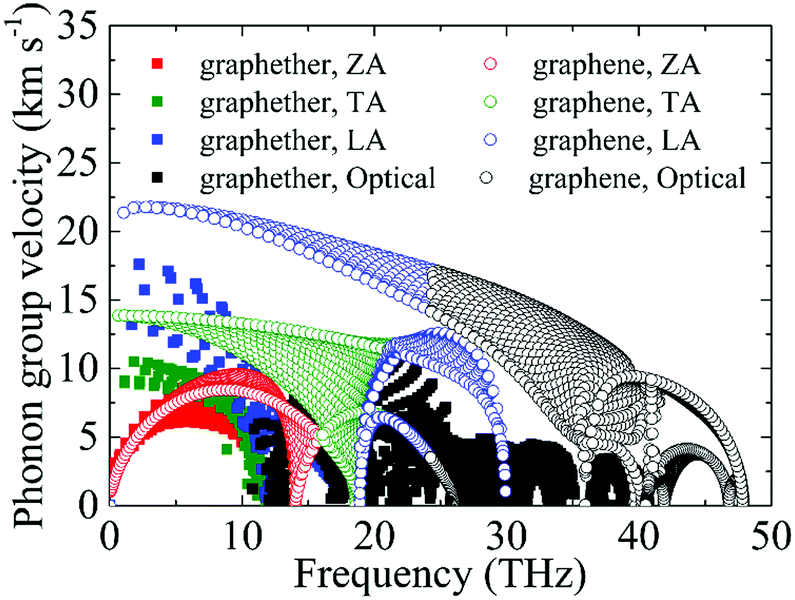
Based on the phonon dispersion curves, the phonon group velocities of graphether and graphene are obtained, which are portrayed in Fig. 8. For graphene, the phonon group velocities of the TA and LA phonon modes near the Γ point are 13.86 km s−1 and 21.36 km s−1, respectively, which are well consistent with previous works (TA: 13.85 km s−1 and LA: 21.59 km s−1).57,58 The corresponding values of graphether are 8.93 km s−1 and 17.60 km s−1. Furthermore, the phonon group velocities of the acoustic phonon modes are higher than those of the optical phonon modes generally in both graphether and graphene. Hence, the acoustic phonon modes have a larger influence on k, which is also in accordance with our aforementioned results (Fig. 4). It can be found that the phonon group velocities of graphether are evidently lower than those of graphene. For intuitive comparison, we compute the average phonon group velocities of graphether and graphene, which are 3.42 km s−1 and 7.09 km s−1, respectively. Consequently, the lower phonon group velocity leads to the lower k in graphether.
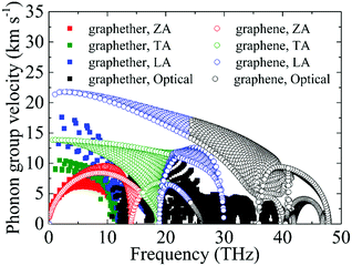 |
| | Fig. 8 The phonon group velocities of different phonon modes in graphether and graphene. | |
3.3 Grüneisen parameter, phase space, phonon lifetime, and phonon mean free path
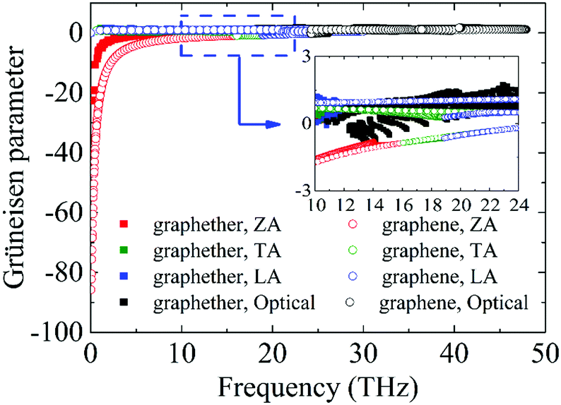
Furthermore, to obtain information about phonon scattering, we explore the Grüneisen parameter and phase space. The Grüneisen parameter provides information about the anharmonicity of phonon modes, and phase space (P3) provides the number of scattering channels for three-phonon processes.59,60 The contributions of different phonon modes to the Grüneisen parameter are illustrated in Fig. 9. It can be observed that the Grüneisen parameter of the ZA phonon mode of graphether is larger than that of graphene. The inset of Fig. 9 shows that the Grüneisen parameter of the LA phonon mode is larger than that of the TA phonon mode in both graphether and graphene. It has been reported that anharmonicity of lattice vibrations is related to an anharmonic phonon–phonon process.61 The larger Grüneisen parameter indicates stronger anharmonicity, which can induce stronger phonon–phonon scattering and a lower k. In addition, the mode weighted accumulative Grüneisen parameters of graphether and graphene are 0.57 and −1.94, respectively, which demonstrates the stronger anharmonic phonon scattering in graphether. The phase space of different phonon modes in graphether and graphene are exhibited in Fig. 10. The P3 of graphether is one order of magnitude larger than that of graphene in the whole frequency range. This result indicates that there are more scattering channels in graphether compared with graphene. A larger P3 means stronger phonon scattering, which results in the lower k of graphether. In addition, as frequency increases, distinct decreases in P3 of graphether and graphene are observed, implying that there are fewer scattering channels in the high frequency region.62
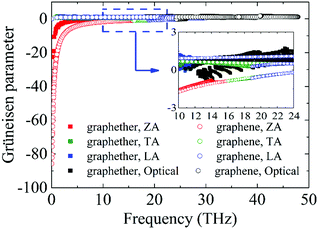 |
| | Fig. 9 The Grüneisen parameters of different phonon modes in graphether and graphene. The inset is the zoom-in figure of the frequency from 10 to 24 THz. | |
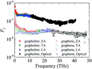 |
| | Fig. 10 The phonon scattering phase space (P3) of different phonon modes in graphether and graphene. | |
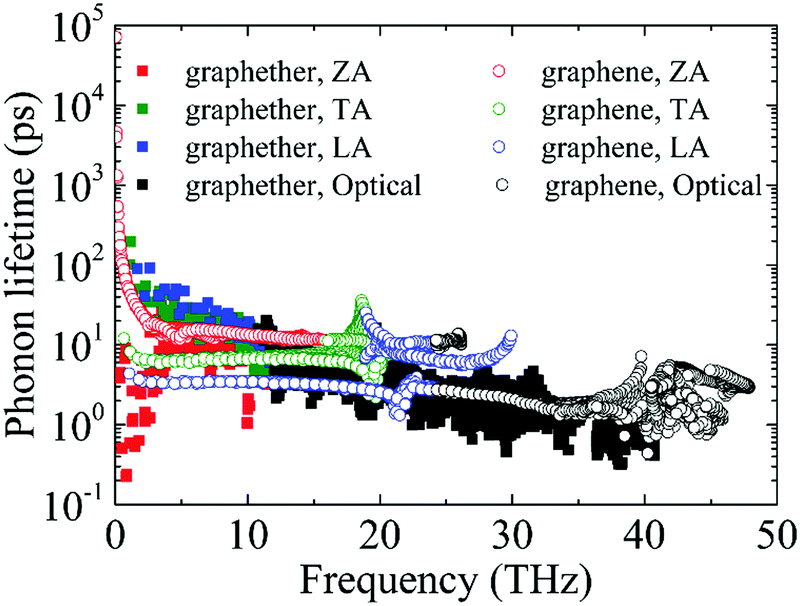
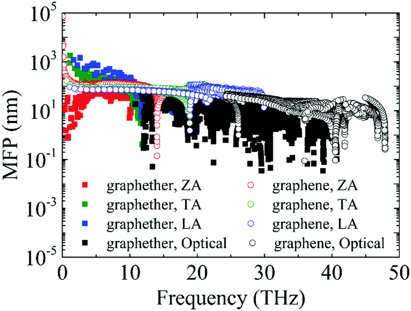
Furthermore, the phonon lifetime as a function of frequency is plotted in Fig. 11, which can give more insight into the phonon transport of graphether and graphene. For graphether, as the phonon frequency increases, the phonon lifetimes of TA and LA phonon modes decrease distinctly, whereas the phonon lifetime of the ZA phonon mode increases firstly and then declines. It should be noted that the TA and LA phonon modes possess a longer phonon lifetime than that of the ZA phonon mode. However, for graphene, the phonon lifetime of the ZA phonon mode is longer than those of the TA and LA phonon modes. Moreover, the phonon lifetime of the ZA phonon mode in graphether is much shorter than that in graphene. It can be also observed that the phonon lifetimes of acoustic phonon modes are several orders of magnitude longer than those of the optical phonon modes, which reveals that the acoustic phonon modes make a greater contribution to k in graphether and graphene. We also compute the average phonon lifetimes of graphether and graphene, which are 4.10 ps and 23.54 ps, respectively. We can ascribe the shorter phonon lifetime to the larger anharmonicity and number of phonon scattering channels, which are described by the Grüneisen parameter and phase space, as shown in Fig. 9 and 10. Therefore, the shorter phonon lifetime leads to the lower k due to the stronger phonon scattering. Here, the phonon MFP displayed in Fig. 12 is obtained by using the formula lλ = νλτλ. When the frequency increases, the phonon MFP generally decreases. The MFPs of acoustic phonon modes are higher than those of the optical phonon modes in both graphether and graphene. Moreover, the cumulative lattice thermal conductivities as a function of phonon mean free paths of graphether and graphene are given in Fig. S4 of the ESI.† It can be observed that at 300 K, k of graphether achieves convergence faster and the corresponding phonon MFP is shorter than that of graphene. In short, the lower lattice thermal conductivity of graphether can be attributed to the lower phonon group velocity and phonon lifetime.
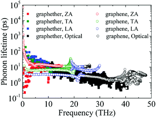 |
| | Fig. 11 The phonon lifetimes of different phonon modes in graphether and graphene. | |
 |
| | Fig. 12 The phonon MFPs of different phonon modes in graphether and graphene at 300 K. | |
3.4 Size effect
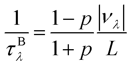
Finally, we further evaluate the size effects of the lattice thermal conductivities of graphether and graphene, which are calculated by considering the phonon-boundary scattering. The phonon-boundary scattering rate is inversely proportional to the system length (L) along the transport direction, which can be given by:63| |  | (2) |
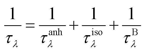
where p is the specularity parameter and L is the system length along the transport direction, respectively. It should be noticed that the parameter p can characterize the roughness of the system edge (p = 0 means an entirely rough boundary and p = 1 indicates an ideal smooth edge). Here, we use a completely diffusive assumption (i.e., p = 0) to model the boundary scatterings of graphether and graphene. Then, the total phonon scattering rate is given by the following formula based on Matthiessen's rule:| | 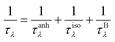 | (3) |
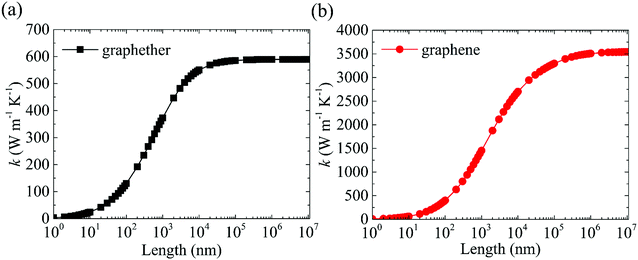
where 1/τλ is the total phonon scattering rate, 1/τanhλ represents the intrinsic anharmonic phonon–phonon scattering rate, 1/τisoλ is the isotopic phonon scattering rate, and 1/τBλ is the phonon-boundary scattering rate. The lattice thermal conductivities of graphether and graphene with respect to different system lengths at 300 K are given in Fig. 13. With the increase of system length, the lattice thermal conductivities of graphether and graphene both increase monotonically and tend to convergent values (i.e., k of materials with an infinite system length). We can observe that the lattice thermal conductivities of graphether and graphene are significantly dependent on the system length, which is consistent with the previous work.64,65 It should also be noted that the effect of system length in graphene is larger than that in graphether, which can be attributed to the longer phonon mean free math of graphene. For example, k of graphether is convergent in the range of 104–105 nm, however k of graphene is almost convergent when the system length is larger than 106 nm.
 |
| | Fig. 13 The length dependences of thermal conductivities of (a) graphether and (b) graphene at 300 K. | |
All in all, we pioneer the probing of the thermal properties of graphether using first-principles calculations. The analysis on phonon behaviors will be beneficial to understanding the nature of phonon transport in graphether. In addition, we evaluate the electron localization function, the electronic band structure, and the stability of graphether in comparison with graphene. Our research will provide fundamental thermal transport information to design graphether-based nanoelectronic devices, which can promote the innovative applications of graphether in next-generation nanoelectronic devices.
4. Conclusions
In summary, the lattice thermal conductivities of graphether and graphene are investigated systematically by combining first-principles calculations and the phonon BTE. The calculated lattice thermal conductivities of graphether and graphene are 600.91 W m−1 K−1 and 3544.41 W m−1 K−1 along the armchair direction at 300 K, respectively. It can be observed that k of graphether is lower than that of graphene. As temperature increases from 200 to 1000 K, the reduction ratios of lattice thermal conductivities in graphether and graphene are 91.65% and 90.47%, respectively. Moreover, the ELFs of graphether and graphene have been calculated. The anisotropic properties of lattice thermal conductivity in graphether along the armchair and zigzag directions are attributed to the anisotropic behaviors of the ELF. Furthermore, the harmonic and anharmonic properties of graphether and graphene are evaluated. The phonon group velocity of graphether is lower than that of graphene, with the average values of 3.42 km s−1 and 7.09 km s−1, respectively. Graphether possesses the shorter phonon lifetime owing to the larger Grüneisen parameters and phase space. The average phonon lifetimes of graphether and graphene are 4.10 ps and 23.54 ps, respectively. We attribute the lower k of graphether to the lower phonon group velocity and phonon lifetime. Furthermore, it is also found that the lattice thermal conductivities of graphether and graphene significantly increase with the length, and k will converge to constant values with the increase of system length. The dependency of the thermal conductivity of graphether on the system length is weaker than that of graphene, which is attributed to the shorter phonon mean free path of graphether. We investigate the lattice thermal conductivity, the electron localization function, the phonon behaviors, and the stability of graphether, and this study extends the application perspective of graphether in 2D nanoelectronic devices.
Conflicts of interest
There are no conflicts of interest to declare.
Acknowledgements
This work is supported by the National Natural Science Foundation of China (No. 51806123), the Natural Science Foundation of Shandong Province, China (No. ZR2018BEE025), the Key R&D Program of Shandong Province, China (No. 2019GGX101030), the China Postdoctoral Science Foundation (No. 2018M642654), and the Fundamental Research Funds of Shandong University, China (No. 2018TB007).
References
- K. S. Novoselov, A. K. Geim, S. V. Morozov, D. Jiang, Y. Zhang, S. V. Dubonos, I. V. Grigorieva and A. A. Firsov, Science, 2004, 306, 666 CrossRef CAS.
- A. K. Geim and K. S. Novoselov, Nat. Mater., 2007, 6, 183–191 CrossRef CAS.
- M. Liu, X. Yin, E. Ulin-Avila, B. Geng, T. Zentgraf, L. Ju, F. Wang and X. Zhang, Nature, 2011, 474, 64–67 CrossRef CAS.
- H. Sun, Z. Xu and C. Gao, Adv. Mater., 2013, 25, 2554–2560 CrossRef CAS.
- A. A. Balandin, S. Ghosh, W. Bao, I. Calizo, D. Teweldebrhan, F. Miao and C. N. Lau, Nano Lett., 2008, 8, 902–907 CrossRef CAS.
- A. B. Bourlinos, V. Georgakilas, R. Zboril, T. A. Steriotis and A. K. Stubos, Small, 2009, 5, 1841–1845 CrossRef CAS.
- J. Xiang and L. T. Drzal, Carbon, 2011, 49, 773–778 CrossRef CAS.
- Q. Yu, J. Lian, S. Siriponglert, H. Li, Y. P. Chen and S. S. Pei, Appl. Phys. Lett., 2008, 93, 193–195 Search PubMed.
- X. Li, X. Wang, L. Zhang, S. Lee and H. Dai, Science, 2008, 319, 1229–1232 CrossRef CAS.
- D. W. Ma, Q. Wang, X. Yan, X. Zhang, C. He, D. Zhou, Y. Tang, Z. Lu and Z. Yang, Carbon, 2016, 105, 463–473 CrossRef CAS.
- D. Han, X. Wang, W. Ding, Y. Chen, J. Zhang, G. Xin and L. Cheng, Nanotechnology, 2019, 30, 075403 CrossRef CAS.
- X. Wu, V. Varshney, J. Lee, T. Zhang, J. L. Wohlwend, A. K. Roy and T. Luo, Nano Lett., 2016, 16, 3925–3935 CrossRef CAS.
- S. M. Hatam-Lee, A. Rajabpour and S. Volz, Carbon, 2020, 161, 816–826 CrossRef CAS.
- X. Wang, J. Zhang, Y. Chen and P. K. L. Chan, Phys. Chem. Chem. Phys., 2017, 19, 15933–15941 RSC.
- X. Wang, M. Wang, Y. Hong, Z. Wang and J. Zhang, Phys. Chem. Chem. Phys., 2017, 19, 24240–24248 RSC.
- G. L. Zhu, X. J. Ye and C. S. Liu, Nanoscale, 2019, 11, 22482–22492 RSC.
- S. Bruzzone and G. Fiori, Appl. Phys. Lett., 2011, 99, 222108 CrossRef.
- B. Peng, H. Zhang, H. Shao, Y. Xu, G. Ni, R. Zhang and H. Zhu, Phys. Rev. B, 2016, 94, 245420 CrossRef.
- H. Zhang, H. Wang, S. Xiong, H. Han, S. Volz and Y. Ni, J. Phys. Chem. C, 2018, 122, 2641–2647 CrossRef CAS.
- S. Baroni, S. de Gironcoli, A. D. Corso and P. Giannozzi, Rev. Mod. Phys., 2001, 73, 515–562 CrossRef CAS.
- G. Deinzer, G. Birner and D. Strauch, Phys. Rev. B: Condens. Matter Mater. Phys., 2003, 67, 144304 CrossRef.
- G. Kresse and J. Furthmüller, Comput. Mater. Sci., 1996, 6, 15–50 CrossRef CAS.
- G. Kresse and J. Furthmüller, Phys. Rev. B: Condens. Matter Mater. Phys., 1996, 54, 11169–11186 CrossRef CAS.
- J. P. Perdew, K. Burke and Y. Wang, Phys. Rev. B: Condens. Matter Mater. Phys., 1996, 54, 16533–16539 CrossRef CAS.
- K. Momma and F. Izumi, J. Appl. Crystallogr., 2011, 44, 1272–1276 CrossRef CAS.
- W. Li, J. Carrete and N. Mingo, Appl. Phys. Lett., 2013, 103, 253103 CrossRef.
- E. Haque and M. A. Hossain, J. Alloys Compd., 2018, 748, 63–72 CrossRef CAS.
- A. Sparavigna, Phys. Rev. B: Condens. Matter Mater. Phys., 2002, 66, 174301 CrossRef.
- A. Ward, D. A. Broido, D. A. Stewart and G. Deinzer, Phys. Rev. B: Condens. Matter Mater. Phys., 2009, 80, 125203 CrossRef.
- W. Li, L. Lindsay, D. A. Broido, D. A. Stewart and N. Mingo, Phys. Rev. B: Condens. Matter Mater. Phys., 2012, 86, 174307 CrossRef.
- B. Peng, H. Zhang, H. Shao, Y. Xu, X. Zhang and H. Zhu, Ann. Phys., 2016, 528, 504–511 CrossRef CAS.
- A. Togo, F. Oba and I. Tanaka, Phys. Rev. B: Condens. Matter Mater. Phys., 2008, 78, 134106 CrossRef.
- N. A. Spaldin, J. Solid State Chem., 2012, 195, 2–10 CrossRef CAS.
- R. M. Pick, M. H. Cohen and R. M. Martin, Phys. Rev. B: Solid State, 1970, 1, 910–920 CrossRef.
- K. Yuan, X. Zhang, L. Li and D. Tang, Phys. Chem. Chem. Phys., 2019, 21, 468–477 RSC.
- X. Wang, Y. Hong, P. K. L. Chan and J. Zhang, Nanotechnology, 2017, 28, 255403 CrossRef.
- X. Wang, J. Zhang, Y. Chen and P. K. L. Chan, Nanoscale, 2017, 9, 2262–2271 RSC.
- H. Sun, Q. Li and X. G. Wan, Phys. Chem. Chem. Phys., 2016, 18, 14927–14932 RSC.
- Y. Hong, J. Zhang, X. Huang and X. C. Zeng, Nanoscale, 2015, 7, 18716–18724 RSC.
- X. Wang, H. Yang, D. Ma and J. Zhang, J. Mater. Chem. C, 2017, 5, 5119–5127 RSC.
- D. Han, W. Ding, X. Wang and L. Cheng, Nanoscale, 2019, 11, 19763–19771 RSC.
- B. Silvi and A. Savin, Nature, 1994, 371, 683–686 CrossRef CAS.
- A. Savin, R. Nesper, S. Wengert and T. F. Fässler, Angew. Chem., Int. Ed. Engl., 1997, 36, 1808–1832 CrossRef CAS.
- P. Chandrachud, B. S. Pujari, S. Haldar, B. Sanyal and D. G. Kanhere, J. Phys.: Condens. Matter, 2010, 22, 465502 CrossRef.
- S. Li, H. Lei, Z. Wang, J. Chen and P. Ruterana, Phys. Status Solidi B, 2018, 255, 1700429 CrossRef.
- J. Heyd and G. E. Scuseria, J. Chem. Phys., 2003, 118, 8207–8215 CrossRef CAS.
- H. Gholivand and N. Donmezer, IEEE Trans. Nanotechnol., 2017, 16, 752–758 CAS.
- K. H. Michel and B. Verberck, Phys. Status Solidi B, 2009, 246, 2802–2805 CrossRef CAS.
- Y. Hong, J. Zhang and X. C. Zeng, Nanoscale, 2018, 10, 4301–4310 RSC.
- E. Mariani and F. V. Oppen, Phys. Rev. Lett., 2008, 100, 076801 CrossRef.
- R. Fei, A. Faghaninia, R. Soklaski, J. A. Yan, C. Lo and L. Yang, Nano Lett., 2014, 14, 6393–6399 CrossRef CAS.
- L. F. Huang, P. L. Gong and Z. Zeng, Phys. Rev. B: Condens. Matter Mater. Phys., 2014, 90, 716–723 Search PubMed.
- C. Xia, W. Li, D. Ma and L. Zhang, Nanotechnology, 2020, 31, 375705 CrossRef CAS.
- B. Mortazavi, M. Makaremi, M. Shahrokhi, M. Raeisi, C. V. Singh, T. Rabczuk and L. F. C. Pereira, Nanoscale, 2018, 10, 3759–3768 RSC.
- E. F. Sheka, N. Popova and V. Popova, Phys.-Usp., 2018, 61, 645–691 CrossRef CAS.
- L. Lindsay, D. A. Broido and N. Mingo, Phys. Rev. B: Condens. Matter Mater. Phys., 2010, 82, 115427 CrossRef.
- Y. Yin, D. Li, Y. Hu, G. Ding, H. Zhou and G. Zhang, Nanotechnology, 2020, 31, 315709 CrossRef CAS.
- D. Han, H. Fan, X. Wang and L. Cheng, Mater. Res. Express, 2020, 7, 035020 CrossRef CAS.
- B. Peng, H. Shao, Y. Xu, X. Zhang and H. Zhu, Sci. Rep., 2016, 6, 20225 CrossRef CAS.
- W. Li, J. Carrete, N. A. Katcho and N. Mingo, Comput. Phys. Commun., 2014, 185, 1747–1758 CrossRef CAS.
- A. Taheri, C. Da Silva and C. H. Amon, Phys. Chem. Chem. Phys., 2018, 20, 27611–27620 RSC.
- L. Lindsay and D. A. Broido, J. Phys.: Condens. Matter, 2008, 20, 165209 CrossRef.
- D. L. Nika, E. P. Pokatilov, A. S. Askerov and A. A. Balandin, Phys. Rev. B: Condens. Matter Mater. Phys., 2009, 79, 155413 CrossRef.
- G. Fugallo, A. Cepellotti, L. Paulatto, M. Lazzeri, N. Marzari and F. Mauri, Nano Lett., 2014, 14, 6109 CrossRef CAS.
- Z. Zhang, Y. Ouyang, Y. Cheng, J. Chen, N. Li and G. Zhang, Phys. Rep., 2020, 860, 1–26 CrossRef CAS.
Footnotes |
| † Electronic supplementary information (ESI) available. See DOI: 10.1039/d0cp03191g |
| ‡ The first author contributed equally to this work. |
|
| This journal is © the Owner Societies 2021 |
Click here to see how this site uses Cookies. View our privacy policy here. 
 *b and
Xinyu
Wang
*b and
Xinyu
Wang