
Chemical vapor deposition of clean and pure MoS2 crystals by the inhibition of MoO3−x intermediates†
Ran
Guan
a,
Junxi
Duan
*b,
Aiheng
Yuan
a,
Zhuofan
Wang
a,
Shuai
Yang
a,
Luoqiao
Han
a,
Bo
Zhang
a,
Dejun
Li
a and
Birong
Luo
 *a
*a
aCollege of Physics and Materials Science, Tianjin Normal University, 300387 Tianjin, P. R. China. E-mail: bluo@tjnu.edu.cn
bSchool of Physics, Beijing Institute of Technology, 100081 Beijing, P. R. China. E-mail: 6120170107@bit.edu.cn
First published on 5th November 2020
Abstract
Molybdenum disulfide (MoS2) synthesized via chemical vapor deposition (CVD) is commonly accompanied by some intermediate products in the form of MoO3−x, resulting in MoS2–MoO3−x hybrids with diverse structures. In this study, we show that through the rational design of heating evaporation rate of the precursors of sulfur and MoO3 separately in a CVD system with double temperature zones, the intermediate product of MoO3−x involved in the CVD growth of MOS2 (generally in the form of quadrilateral MoO2/MoS2 composites and/or stacks of quadrilateral MoO2/triangular MoS2) can be inhibited largely. On this basis, the appropriate sulfur sublimation versus the evaporated MoO3 powder is revealed to be the key factor for the inhibition of intermediates, obtaining high-quality MoS2 crystals with as high as >90% cleanness/purity. This study will assist our understanding of the fundamental CVD growth mechanisms of transition metal dichalcogenides (TMDCs) and provides a facile direction for the controlled synthesis of high-quality MoS2 and other TMDCs with or without intermediate hybrids for applications.
1 Introduction
As a typical transition metal dichalcogenide (TMDC), layered MoS2 has attracted extensive attention due to its unique material properties and various potential applications in nanoelectronics1–5 and optoelectronics6,7etc. Simultaneously, numerous efforts have also been devoted to the synthesis of MoS2 films, notably via chemical vapor deposition (CVD),8–13 which can produce large-area MoS2 layers with decent quality as a counterpart with respect to the mechanical exfoliation method. In general, the CVD process employed for the synthesis of MoS2 involve the use of solid sulfur and molybdenum oxide powder (e.g., MoO3) as the precursors, and it has been shown that controlling the reaction conditions in the CVD growth is of significance for obtaining large-area and high-quality MoS2 layers.14,15 There have been many attempts to control the growth processes by changing the relative position of the growth substrates and the precursor,14,16 or by regulating the carrier gas flow17,18 and growth temperature.19 Despite the enormously experimental progress, some processes involved in the formation of clean and pure MoS2 layers during such a CVD reaction between the precursors is still unclear. For instance, there remains a lack of mechanistic understanding of the factors that control the sulfurized purity and micro/nano-hybrid structures of the grown MoS2. Indeed, it is a common problem with the CVD growth of MoS2 that the finally grown products would be accompanied by some contaminants or intermediates of MoO3−x, thus making the occurrence of both pure MoS2 layers and hybrid MoS2–MoO3−x structures (such as core–shell structured MoO2–MoS2).19,20 Hence, it is highly desirable to reveal the mechanisms on how to controllably grow clean and pure MoS2 crystals, and MoS2–MoO3−x hybrids, respectively, for different synthesis target.Here, in this study, we present an optimized growth direction for synthesizing uniform, pure and clean MoS2 crystals in large scale by the inhibition of the intermediate products of MoO3−x involved in the CVD growth of MoS2. Through the improvement of the heating sublimation rate of sulfur at a certain evaporated MoO3 atmosphere near the growth substrates, the formation of composites having mixed structures of MoO3−x–MoS2 (mainly MoO2–MoS2) could be inhibited largely, and then pure and clean MoS2 crystals in large scale were obtained on the Si/SiO2 substrates. Further, their electrical performance was measured, which showed a decent field effect transistor (FET) carrier mobility and on/off ratio. Under the guidance of analyzing the CVD reaction processes and kinetics between sulfur and MoO3 precursor, we are able to attribute this inhibition of the intermediates to a relatively high atmosphere ratio between sulfur and MoO3/MoO3−x vapor, which would result in the complete transformation of the thermally decomposed MoO3−x vapor into MoS2 within a stable and supersaturation of sulfur atmosphere even at fast kinetic reactions at high temperatures. In addition, a series of vertical stacking structures of the layered MoO2–MoS2 hybrids could be obtained as well by controlling the sulfur atmosphere with respect to the MoO3 vapor. This study reveals a CVD reactive mechanism for completely converting MoO3/MoO3−x into MoS2 and will provide a direction for enabling both the synthesis of clean and pure MoS2 crystals, and vertically structured MO2–MoS2 hybrids for potential applications. More important, it will assist in our understanding of the fundamental CVD growth mechanisms of TMDCs for optimizing synthesis.
2 Experimental section
2.1 CVD growth of pure, clean MoS2 and MoO3−x–MoS2 hybrids
The experiment adopts the tube furnace with a double temperature zone, comprising of low temperature heating zone and high temperature heating zone. Sulfur powder (20 mg, 99.98%, Sigma-Aldrich) was loaded in a separate quartz boat located at the low temperature heating zone, which is 29 cm away from the MoO3 (4 mg, 99.97%, Sigma-Aldrich) containing boat. Growth substrates were silicon with a 300 nm layer of SiO2. Substrates were cleaned via ultra-sonication in acetone and IPA for 15 min, respectively, followed by N2 drying. After that, the cleaned silicon substrates (300 nm-SiO2/Si) were placed upside down on the quartz boat directly above the MoO3 source. The schematic for the experiment is shown in Fig. 1a. Before starting the CVD growth, the CVD system was pumped down to ∼0.1 Pa, and then the quartz tube was filled with Ar gas and pumped again. This was repeated three times to exhaust the air and impurities in the quartz tube as far as possible. For the CVD growth, the furnaces were heated up to 120 °C and 880 °C in 20 min, respectively, under atmospheric pressure with 200 sccm Ar flowing. Then, the first furnace was heated at a varied rate (1, 5, 8 °C min−1) for 10 min to the desired temperature, while the second furnace was held at 880 °C for 10 min growth. After the growth, the system was cooled down to the room temperature by simply opening the furnaces.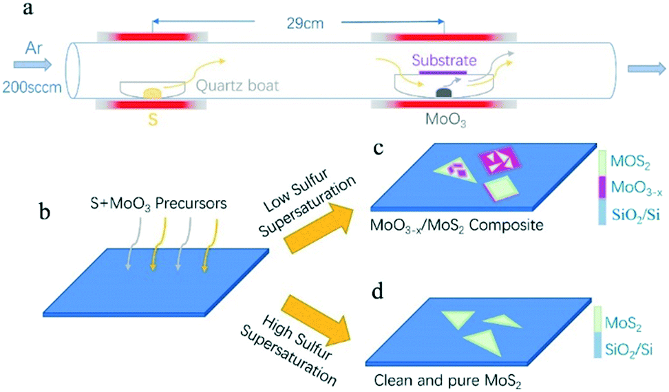 | ||
| Fig. 1 (a) Schematic of the CVD system that is divided by low and high temperature zones. (b) Schematic illustration of the CVD synthesis of (c) MoS2–MoO3−x composites and (d) clean, pure MoS2 crystals on SiO2/Si, respectively, using S and MoO3 precursors. | ||
2.2 Direct synthesis of MoO3−x intermediate products without S precursor
Here, only the second furnace was used for the synthesis of MoO3−x intermediate products. 4 mg MoO3 powder was put in the quartz boat, which was covered by a growth substrate. The furnace was then heated up to 880 °C within 20 min at 200 sccm Ar flowing under atmospheric pressure. After holding the temperature for 10 min, the furnace was cooled to the room temperature by opening the furnace.2.3 Characterization methods
The features of the as-grown pure and clean MoS2 layers and MoS2–MoO3−x composites were characterized via optical microscopy, scanning electron microscopy (SEM, JEOL, JSM-6390A at 15 kV), X-ray diffraction (XRD, Bruker, D8 Advance with a Cu Kα X-ray source), and Raman spectroscopy (HORIBA microscope under ambient conditions using a 514 nm excitation laser source).2.4 Monolayer clean MoS2-based device fabrication
Monolayer MoS2-based FETs on SiO2 were defined and patterned via electron beam lithography (EBL), followed by the electron beam evaporation of Ti/Au (5 nm/45 nm) and lift-off. Devices were electrically tested using a Keithley 4200 semiconductor parameter analyzer at room temperature at ambient condition.3 Results and discussion
Fig. 1a shows the main configurations of the CVD system used for the growth of MoS2. As shown, the samples were grown by CVD with solid S and MoO3 powders in an Ar atmospheric pressure. The growth substrate (SiO2/Si) faced down to MoO3 powder. In theory, the powder-based CVD growth of MoS2 would undergo a series of thermal-dynamics and chemical processes, which can be denoted by these chemical reaction equations:21| 2MoO3 + xS → 2MoO3−x + xSO2 | (1) |
| 2MoO3−x + (7 − x)S → 2MoS2 + (3 − x)SO2 | (2) |
| 2MoO3 + 7S → 2MoS2 + 3SO2 | (3) |
Therefore, here, two independent furnaces were used to precisely control the temperature of S and MoO3 with a specific heating rate. This is important for the control over the sublimation of S and the evaporation of MoS3, respectively, and then determination of the CVD products. In detail, the temperature for S and MoO3 powder was ramped to 120 °C (slightly higher than the sulfur melting point of 112.8 °C) and 880 °C in 20 min, respectively. This temperature ramp would ensure the full evaporation of solid MoO3 and provide an active environment with high diffusivity of the precursor and increased number of the active MoO3−x intermediates.22 The followed growth time was set to be 10 min at 880 °C; meanwhile, the S powder was further heated up in varied ramping rates (1, 5, 8 °C min−1) during 10 min growth time, as shown in Fig. 2a–c. The varied ramping rate would produce different quantity of the sublimated S vapor, which would cause different CVD growth products. For instance, the ramp rate of 1 °C min−1 (Fig. 2a) would produce a S-poor environment with low S concentration, resulting in an insufficient sulfurization of the MoO3−x intermediates, finally forming MoO3−x–MoS2 composites (see Fig. 2d and g). As shown in Fig. 2d and g, quadrilateral MoO3−x–MoS2 composites with different nucleation densities could be found in the substrate center and edge due to the location effect of the precursor diffusion.23–25 When the heating ramp rate of S came to 5 °C min−1 (Fig. 2b), the CVD products would change to MoO3−x–MoS2 stacks (Fig. 2c and h), showing quadrilateral MoO3−x stacked with triangular MoS2, as shown in the inset of Fig. 2c and h. Further increasing the heating ramp rate of S to 8 °C min−1 (Fig. 2c), almost clean and pure MoS2 crystals would be obtained in both of the substrate center (Fig. 2f) and edges (Fig. 2i), just with different layers.
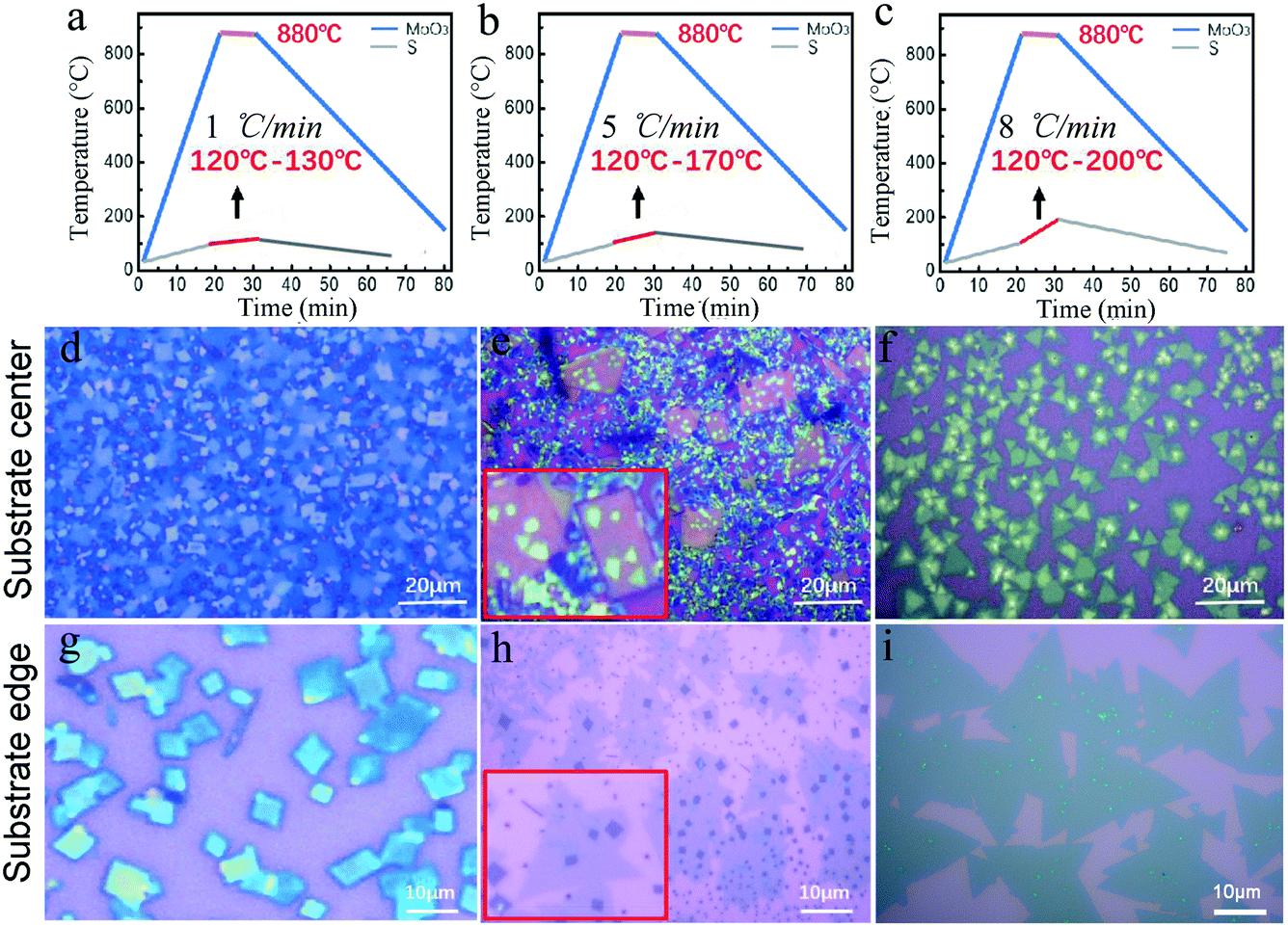 | ||
| Fig. 2 Temperature ramping processes of the MoO3 and S precursors as a function of time with different heating rates of the S during growth: (a) 1 °C min−1, (b) 5 °C min−1, and (c) 8 °C min−1. (d–i) Optical images of as-grown (d and g) MoO3−x–MoS2 composites, (e and h) stacks of quadrilateral MoO3−x/triangular MoS2, and (f and i) clean triangular MoS2 grains at the center and edge of the SiO2/Si substrate using different S heating rates ((d and g) 1 °C min−1, (e and h) 5 °C min−1, and (f and i) 8 °C min−1). | ||
Fig. 3a–c show the deposited pattern transition of the sample as the heating rate of S increases gradually in Fig. 2. Heating S with a low sublimation rate results in an insufficient S reduction atmosphere for MoO3, which allows the evaporated MoO3 and MoO3−x preferentially nucleate and grow on the substrate in kind of quadrilateral shapes. When almost all the MoO3 precursor was consumed, the S vapor was transported to the surface of the quadrilateral MoO3−x, sulfurization of MoO3−x would occur and MoS2 layers would be formed on the top (schematically shown in Fig. 3a). It should be noted that the MoS2 layers on top would hinder the further reaction between MoO3−x and S vapor, forming quadrilateral MoO3−x–MoS2 composites as experimentally shown above (Fig. 2d and g). With the increase in the S heating rate, triangular MoS2 sheet can be formed and deposited on top of quadrilateral MoO3−x, forming stacks of quadrilateral MoO3−x and triangular MoS2 (schematically shown in Fig. 3b). With further rapid increase in the S heating rate, the appropriate ratio between S and MoO3−x vapor would be meted, and the evaporated MoO3−x would be completely transformed to be clean and pure MoS2 crystals, as schematically shown in Fig. 3c. Alternatively, the increased S ramping rate during the growth time would produce different quantities of sublimated S vapor and enable a transition of the reaction environment from being S-poor to S-rich, which induce the corresponding change of products from the MoO3−x–MoS2 composites to stacks of quadrilateral MoO3−x/triangular MoS2, then ultimately to clean and pure triangular MoS2 (Fig. 3a–c).
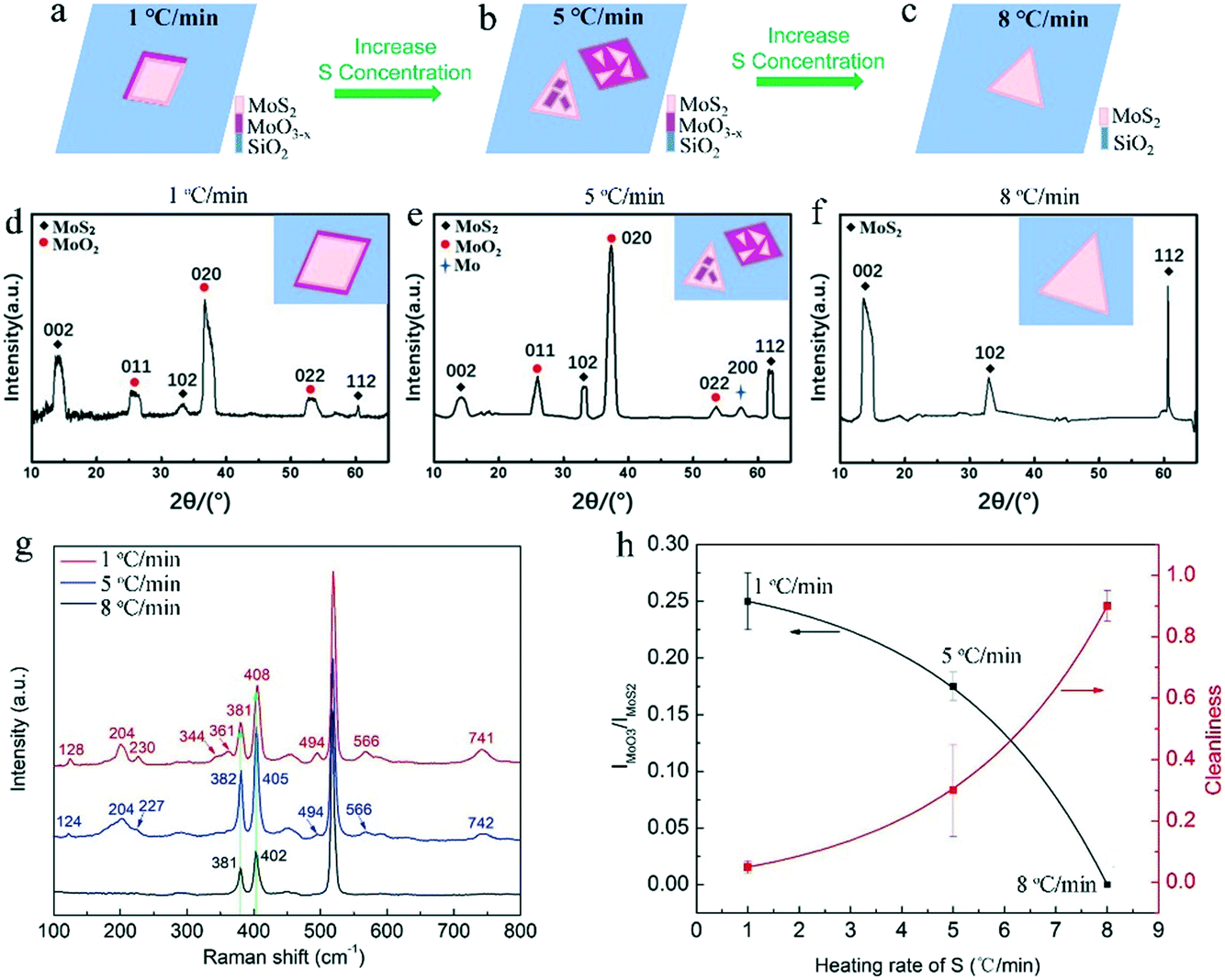 | ||
| Fig. 3 (a–c) Schematic evolution of the deposited patterns of sample prepared by gradually increasing the heating rate of S during the growth from (a) 1 °C min−1 to (b) 5 °C min−1, and finally to (c) 8 °C min−1. (d) XRD patterns of the samples prepared by gradually increasing the heating rate of S during the growth from 1 °C min−1 to (e) 5 °C min−1, and finally to (f) 8 °C min−1. (g) Raman spectra of deposited samples corresponding to the pattern in (a)–(c). (h) The fitted curves of the Raman intensity ratio of IMoO2/IMoS2 at ∼494 and ∼381 cm−1 and the corresponding cleanness with respect to the heating rate of S during the growth. | ||
In order to conform what MoO3−x exactly is, Raman spectroscopy and X-ray diffraction (XRD) were employed for measuring these grown samples. Fig. 3d–g is the typical XRD pattern and Raman spectra for the as-grown quadrilateral MoO3−x–MoS2 composites, stacks of quadrilateral MoO3−x/triangular MoS2, and clean, pure triangular MoS2 crystals (Fig. 2d–i), which corresponds to 1, 5, 8 °C min−1 heating rates of S and the configuration patterns in Fig. 3a–c, respectively. As shown in Fig. 3d–f, all the XRD patterns show characteristic diffraction peaks at ∼14.0° (002), ∼33.0° (102), and ∼60.7° (112), confirming the existence of the MoS2 phase (JCPDS No. 75-1539)26,27 in all the samples. Particularly, there are obvious diffraction peaks (∼26.0° (011), ∼37.3° (020), and ∼53.5° (022)) present in both the samples of quadrilateral MoO3−x–MoS2 composites (Fig. 3d) and stacks of quadrilateral MoO3−x/triangular MoS2 (Fig. 3e), which are ascribed to the MoO2 phase (JCPDS No. 86-0135).26,27 On the other hand, the typical Raman spectra (Fig. 3g) demonstrate obvious Raman characteristics of E2g1 and A1g for MoS2,28,29 which are assigned to the in-plane vibration of molybdenum and sulfur atoms (E2g1), and the out-of-plane vibration of sulfur atoms (A1g),30 respectively. It is necessary to note that the difference between E2g1 and A1g (Δk = A1g − E2g1), which can be employed to discriminate the layers number of MoS2,28,29,31,32 shows differences for each here. As shown, Δk for the sample grown at the 1, 5, and 8 °C min−1 heating rates of S is 27, 23, and 21 cm−1 (also see the summarized results in Table S1†), respectively, which demonstrates that the layers number of MoS2 here are changed from multi-layer to mono-layer28 with the increase in the S heating rate from 1, to 5 and finally to 8 °C min−1. This is due to a different reaction mechanism, where a high S heating rate with an appropriate ratio between S and MoO3−x vapor would react in a thermodynamically stable process22 for the diffusion of Mo and S atoms to the energetically favourable sites, and forming thin MoS2 layer. On the contrary, a low S heating rate with insufficient S to MoO3−x vapor would cause the formation and deposition of MoO3−x intermediates with sulfurized thick top layers of MoS2. More importantly, there are many other peaks appearing in the Raman spectra of the samples of quadrilateral MoO3−x–MoS2 composites (located at 128, 204, 230, 344, 361, 494, 566, 741 cm−1) and stacks of quadrilateral MoO3−x/triangular MoS2 (located at 124, 204, 227, 494, 566, 742 cm−1). These peaks are assigned to the Raman characteristics of MoO2 (ref. 9, 13, 33) and/or MoOS2,34 which are absent in the Raman spectrum for the sample of clean and pure MoS2 crystals prepared at the rapid heating rate of S (8 °C min−1) during the growth. All the results from Raman characterization are summarized in the Table S1 in the ESI.† These XRD and Raman features confirm that the general MoO3−x intermediates generated here during the growth are mainly MoO2 and/or MoOS2 due to a stepwise sulfurization to convert MoO3 into MoS2.34 Further, based on these Raman features, the Raman intensity ratio of IMoO2/IMoS2 at ∼494 and ∼381 cm−1 is plotted and fitted (Fig. 3h black curve), showing a decreasing tendency of MoO2 (increase tendency of MoS2) with the increase in the heating rate of S. Simultaneously, the corresponding cleanness/purity of the as-prepared samples can be plotted and fitted as well with the increase of heating rate of S during the growth. As shown in Fig. 3h (red curve), the cleanness/purity of the sample prepared increases with the increase in the heating rate of S during the growth. The cleanness/purity of the sample prepared at the 8 °C min−1 heating rate of S during the growth can be as high as 90% (Fig. 3h). Indeed, all of these XRD and Raman results indicate that an appropriate ratio between sublimated S and evaporated MoS3 during the growth is the key factor for the inhibition of MoO3−x intermediates and determination of the final products with clean and pure MoS2 crystals.
In addition, an S-free CVD process with only MoO3 precursor (the setup and growth processes can be seen in Fig. S1a and b†) was conducted to indirectly explore the existence of MoO3−x intermediates. The optical (Fig. S2a†) and SEM (Fig. S2b†) images show that the quadrilateral and striped shapes of the products are grown and distributed on the substrate after growth. Further, the corresponding Raman spectrum of the obtained product show the Raman characteristic peaks (128, 230, 343, 361, 494, 566, and 742 cm−1) of MoO2 (Fig. S2c†), which are almost the same with that of the quadrilateral MoO3−x–MoS2 composites grown at 1 °C min−1 heating rate of S, as we discussed above. This indicates that here the as-prepared sample without S was mainly MoO2. In particular, after the post-sulfurization of the sample, MoO2 could be transformed into quadrilateral MoO2–MoS2 composites as well (Fig. S3a and b†), which was confirmed by the presence of Raman A1g and E2g1 features of MoS2 in their Raman spectra (Fig. S3c†). This agrees well with the growth mechanism we proposed with S-poor environment: the MoO3 precursor would be consumed first and transform into MoO3−x (mainly MoO2) in an S-poor environment, followed by sulfurization on the top layers, forming MoO3−x–MoS2 hybrids.
Some larger clean and pure MoS2 crystals were chosen for the detailed Raman spectroscopy and AFM characterizations (Fig. 4). As shown, two characteristic Raman vibration modes E2g1 and A1g with a frequency difference Δk of 19 cm−1 can be seen in the spectrum in Fig. 4a. This frequency difference Δk is slightly changed compared with the Raman data (21 cm−1) in Fig. 3g due to the sample difference. This matches well with the frequency difference of the CVD-grown monolayer MoS2 in a previous work.35 The full width at half-maximum (FWHM) of the E2g1 peak is 3.8 cm−1, which is close to that of the exfoliated monolayer MoS2, 3.7 cm−1, suggesting good crystalline quality of the clean and pure monolayer crystals here. We also performed Raman mapping on a corner for the large triangular MoS2 crystal (inset of Fig. 4a) by plotting the Raman intensity map of the A1g (Fig. 4b) and E2g1 (Fig. S4†) peaks to show the characteristic uniformity of a large area. Fig. 4c and d give a typical AFM measurement, showing the triangular topography (Fig. 4c) with a thickness of the edge ∼0.8 nm (Fig. 4d). This layer thickness is in the range of a single-layer MoS2 film on the bare substrates.24,36
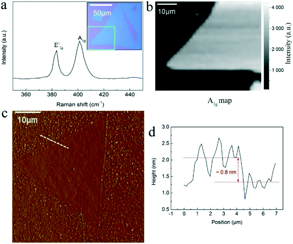 | ||
| Fig. 4 (a) Raman spectrum of the clean and pure MoS2 crystals. The inset is the corresponding optical image of the clean and pure MoS2 crystals. (b) The A1g intensity Raman map corresponding to the corner area of the clean and pure MoS2 crystals shown in the upper right of panel (a). (c) AFM topography image and (d) the correlated height profile taken across the dotted white line in (c), respectively, for a clean and pure MoS2 crystals. | ||
To further evaluate the quality of the as-obtained clean and pure MoS2, the back-gated field-effect transistor (FET) devices were directly constructed and fabricated based on these monolayer clean and pure MoS2 crystals. Their fabrications were based on previous reports,37–39 and briefly described in the experimental section. Fig. 5a is the optical image of the fabricated FET devices, which is also schematically shown in Fig. 5b, showing the structural configuration on the SiO2/Si substrate using Ti/Au as the source-drain (S-D) electrodes. A typical device numbered with ① is optically shown with high-magnification in the Fig. 5c. As shown, the ratio between specific channel length and width (L/W) is ∼8 μm/13 μm.
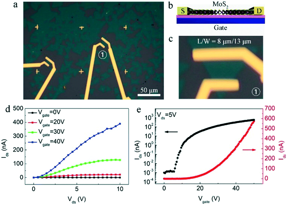 | ||
| Fig. 5 (a) Optical image of the FET devices based on as-grown clean and pure MoS2 crystals. (b) Schematic of the FET device configuration based on the MoS2 layer. (c) The high-magnification optical image of the FET device numbered with ① in (a). (d) Output characteristics (Ids–Vds) of the FET device with respect to the back-gate voltage at 0, 20, 30, and 40 V, respectively. (e) Transfer characteristics curves (Ids–Vgate) of the FET device at 5 V D–S voltage. | ||
The electrical transport measurements of the fabricated devices were conducted under ambient conditions. Fig. 5d is the typical output characteristics (Ids–Vds) of the FET device at various gate voltage Vbg (0, 20, 30, and 40 V) under ambient conditions, and the nonlinear output characteristics suggest the existence of a small Schottky barrier between the Ti/Au metal contacts and MoS2 layer.40 The transfer characteristics (Ids–Vgate) of the MoS2 device at various S-D voltages are shown in Fig. S5.† As shown, the Ids value increases monotonically with the increase in Vgate, indicating an n-type semiconducting behavior. Specifically, the transfer curve at the 5 V S-D voltage (Vds = 5 V) is plotted in Fig. 5e (red curve), and the FET mobility could be extracted based on the linear region of the transfer curve according to the formula, μFE = Lchgm/WchCoxVds, where Lch, and Wch are the device channel length and width, respectively, gm is the transconductance of MoS2 that can be extracted by performing a linear fit in the Ids–Vgate curve, Vds is the S-D voltage, Cox is the gate capacitance of SiO2 dielectrics. This yields electron mobility of ∼4 cm−2 V−1 s−1 with an observed current modulation Ion/Ioff ratio of ∼106 by plotting the Ids–Vgate curve on a logarithmic scale (black curve in Fig. 5e). The electron mobilities of all the devices we measured are in the range of 1–12 cm−2 V−1 s−1. These results demonstrate that here the as-obtained clean and pure MoS2 crystals possess decent quality with large scale. It is necessary to note that the mobility could be improved by measuring the device under certain conditions (or by other treatments) such as low-temperature, vacuum, and high-k top gate dielectric treatment and interface engineering.12,41,42
4 Conclusions
In conclusion, we have successfully realized the growth of clean and pure MoS2 crystals by the inhibitation of MoO3−x intermediates in a powder-based CVD method. Through rational design of the heating rate of S from low S supersaturating to a high S supersaturating environment during the growth process, a series of CVD products transformed from the quadrilateral MoO3−x/MoS2 composites to stacks of quadrilateral MoO3−x/triangular MoS2, and finally to clean, pure triangular MoS2 crystals could be obtained. Various characterization techniques confirmed that the intermediate of MoO3−x is mainly MoO2, which could be inhibited largely by appropriate ratio between the sublimated S and evaporated MoO3 vapor. Further, the electrical transport measurements indicate that the as-synthesized clean and pure MoS2 crystals have high quality with decent FET electron mobility. This work will assist in our understanding of the fundamental CVD growth mechanisms of TMDCs and provide a growth-optimized direction for the synthesis of clean and pure TMDCs crystals.Conflicts of interest
There are no conflicts to declare.Acknowledgements
Birong Luo acknowledges financial support from Natural Science Foundation of Tianjin (20JCYBJC00350), the 13th Tianjin Thousand Youth Talents Plan Project (ZX0471800601) and generous start-up funding from Tianjin Normal University (YJRL201904).References
- H. Zeng, J. Dai, W. Yao, D. Xiao and X. Cui, Nat. Nanotechnol., 2012, 7, 490–493 CrossRef.
- M. Chhowalla, H. S. Shin, G. Eda, L.-J. Li, K. P. Loh and H. Zhang, Nat. Chem., 2013, 5, 263–275 CrossRef.
- M. Belete, S. Kataria, U. Koch, M. Kruth, C. Engelhard, J. Mayer, O. Engstrom and M. C. Lemme, ACS Appl. Nano Mater., 2018, 1, 6197–6204 CrossRef.
- H. Y. Chang, M. N. Yogeesh, R. Ghosh, A. Rai, A. Sanne, S. Yang, N. Lu, S. K. Banerjee and D. Akinwande, Adv. Mater., 2016, 28, 1818–1823 CrossRef.
- Q. H. Wang, K. Kalantar-Zadeh, A. Kis, J. N. Coleman and M. S. Strano, Nat. Nanotechnol., 2012, 7, 699–712 CrossRef.
- P. Yang, Z. Zhang, M. Sun, F. Lin, T. Cheng, J. Shi, C. Xie, Y. Shi, S. Jiang, Y. Huan, P. Liu, F. Ding, C. Xiong, D. Xie and Y. Zhang, ACS Nano, 2019, 13, 3649–3658 CrossRef.
- E. Singh, P. Singh, K. S. Kim, G. Y. Yeom and H. S. Nalwa, ACS Appl. Mater. Interfaces, 2019, 11, 11061–11105 CrossRef.
- Y.-H. Lee, X.-Q. Zhang, W. Zhang, M.-T. Chang, C.-T. Lin, K.-D. Chang, Y.-C. Yu, J. T.-W. Wang, C.-S. Chang, L.-J. Li and T.-W. Lin, Adv. Mater., 2012, 24, 2320–2325 CrossRef.
- H. F. Liu, S. L. Wong and D. Z. Chi, Chem. Vap. Deposition, 2015, 21, 241–259 CrossRef.
- G. H. Han, N. J. Kybert, C. H. Naylor, B. S. Lee, J. Ping, J. H. Park, J. Kang, S. Y. Lee, Y. H. Lee, R. Agarwal and A. T. C. Johnson, Nat. Commun., 2015, 6, 6128 CrossRef CAS.
- V. Kranthi Kumar, S. Dhar, T. H. Choudhury, S. A. Shivashankar and S. Raghavan, Nanoscale, 2015, 7, 7802–7810 RSC.
- J. Chen, W. Tang, B. Tian, B. Liu, X. Zhao, Y. Liu, T. Ren, W. Liu, D. Geng, H. Y. Jeong, H. S. Shin, W. Zhou and K. P. Loh, Adv. Sci., 2016, 3, 1500033 CrossRef.
- X. Wang, H. Feng, Y. Wu and L. Jiao, J. Am. Chem. Soc., 2013, 135, 5304–5307 CrossRef CAS.
- A. Govind Rajan, J. H. Warner, D. Blankschtein and M. S. Strano, ACS Nano, 2016, 10, 4330–4344 CrossRef CAS.
- Y. H. Lee, X. Q. Zhang, W. Zhang, M. T. Chang, C. T. Lin, K. D. Chang, Y. C. Yu, J. T. Wang, C. S. Chang, L. J. Li and T. W. Lin, Adv. Mater., 2012, 24, 2320–2325 CrossRef CAS.
- S. Wang, M. Pacios, H. Bhaskaran and J. H. Warner, Nanotechnology, 2016, 27, 085604 CrossRef.
- M. A. Nikpay, S. Z. Mortazavi, A. Reyhani and S. M. Elahi, Opt. Quantum Electron., 2018, 50, 252 CrossRef.
- H. Liu, Y. Zhu, Q. Meng, X. Lu, S. Kong, Z. Huang, P. Jiang and X. Bao, Nano Res., 2017, 10, 643–651 CrossRef CAS.
- T. Park, M. Leem, H. Lee, W. Ahn, H. Kim, J. Kim, E. Lee, Y.-H. Kim and H. Kim, J. Phys. Chem. C, 2017, 121, 27693–27699 CrossRef CAS.
- S. S. Withanage, H. Kalita, H. S. Chung, T. Roy, Y. Jung and S. I. Khondaker, ACS Omega, 2018, 3, 18943–18949 CrossRef CAS.
- N. K. Perkgoz and M. Bay, Nano-Micro Lett., 2016, 8, 70–79 CrossRef.
- J. Lee, S. Pak, P. Giraud, Y.-W. Lee, Y. Cho, J. Hong, A.-R. Jang, H.-S. Chung, W.-K. Hong, H. Y. Jeong, H. S. Shin, L. G. Occhipinti, S. M. Morris, S. Cha, J. I. Sohn and J. M. Kim, Adv. Mater., 2017, 29, 1702206 CrossRef.
- A. M. van der Zande, P. Y. Huang, D. A. Chenet, T. C. Berkelbach, Y. You, G.-H. Lee, T. F. Heinz, D. R. Reichman, D. A. Muller and J. C. Hone, Nat. Mater., 2013, 12, 554–561 CrossRef CAS.
- S. Wang, Y. Rong, Y. Fan, M. Pacios, H. Bhaskaran, K. He and J. H. Warner, Chem. Mater., 2014, 26, 6371–6379 CrossRef CAS.
- H. Schmidt, S. Wang, L. Chu, M. Toh, R. Kumar, W. Zhao, A. H. Castro Neto, J. Martin, S. Adam, B. Özyilmaz and G. Eda, Nano Lett., 2014, 14, 1909–1913 CrossRef CAS.
- Y. Huang, X. Xie, Y. Zhang, J. Ding, L. Liu, Y. Fan, H. Lv, Y. Liu and Q. Cai, Appl. Surf. Sci., 2020, 520, 146340 CrossRef.
- J. Zhou, N.-S. Xu, S.-Z. Deng, J. Chen, J.-C. She and Z.-L. Wang, Adv. Mater., 2003, 15, 1835–1840 CrossRef CAS.
- H. Li, Q. Zhang, C. C. R. Yap, B. K. Tay, T. H. T. Edwin, A. Olivier and D. Baillargeat, Adv. Funct. Mater., 2012, 22, 1385–1390 CrossRef CAS.
- S. Najmaei, Z. Liu, P. M. Ajayan and J. Lou, Appl. Phys. Lett., 2012, 100, 013106 CrossRef.
- P. Tonndorf, R. Schmidt, P. Bottger, X. Zhang, J. Borner, A. Liebig, M. Albrecht, C. Kloc, O. Gordan, D. R. T. Zahn, S. M. de Vasconcellos and R. Bratschitsch, Opt. Express, 2013, 21, 4908–4916 CrossRef CAS.
- M. Boukhicha, M. Calandra, M.-A. Measson, O. Lancry and A. Shukla, Phys. Rev. B: Condens. Matter Mater. Phys., 2013, 87, 195316 CrossRef.
- F. Bonaccorso, P.-H. Tan and A. C. Ferrari, ACS Nano, 2013, 7, 1838–1844 CrossRef CAS.
- M. A. Camacho-López, L. Escobar-Alarcón, M. Picquart, R. Arroyo, G. Córdoba and E. Haro-Poniatowski, Opt. Mater., 2011, 33, 480–484 CrossRef.
- J. V. Pondick, J. M. Woods, J. Xing, Y. Zhou and J. J. Cha, ACS Appl. Nano Mater., 2018, 1, 5655–5661 CrossRef CAS.
- N. Kumar, R. Tomar, N. Wadehra, M. M. Devi, B. Prakash and S. Chakraverty, Cryst. Res. Technol., 2018, 53, 1800002 CrossRef.
- C. Lee, H. Yan, L. E. Brus, T. F. Heinz, J. Hone and S. Ryu, ACS Nano, 2010, 4, 2695–2700 CrossRef CAS.
- B. Luo, B. Chen, L. Meng, D. Geng, H. Liu, J. Xu, Z. Zhang, H. Zhang, L. Peng and L. He, Adv. Mater., 2014, 26, 3218–3224 CrossRef CAS.
- B. R. Luo, J. M. Caridad, P. R. Whelan, J. D. Thomsen, D. M. A. Mackenzie, A. G. Cabo, S. K. Mahatha, M. Bianchi, P. Hofmann, P. U. Jepsen, P. Boggild and T. J. Booth, 2D Mater., 2017, 4, 045017 CrossRef.
- J. Duan, X. Wang, X. Lai, G. Li, K. Watanabe, T. Taniguchi, M. Zebarjadi and E. Y. Andrei, Proc. Natl. Acad. Sci. U. S. A., 2016, 113, 14272–14276 CrossRef CAS.
- Y.-H. Lee, L. Yu, H. Wang, W. Fang, X. Ling, Y. Shi, C.-T. Lin, J.-K. Huang, M.-T. Chang, C.-S. Chang, M. Dresselhaus, T. Palacios, L.-J. Li and J. Kong, Nano Lett., 2013, 13, 1852–1857 CrossRef CAS.
- W. Chen, J. Zhao, J. Zhang, L. Gu, Z. Yang, X. Li, H. Yu, X. Zhu, R. Yang, D. Shi, X. Lin, J. Guo, X. Bai and G. Zhang, J. Am. Chem. Soc., 2015, 137, 15632–15635 CrossRef CAS.
- S. Das, H.-Y. Chen, A. V. Penumatcha and J. Appenzeller, Nano Lett., 2013, 13, 100–105 CrossRef CAS.
Footnote |
| † Electronic supplementary information (ESI) available. See DOI: 10.1039/d0ce01354d |
| This journal is © The Royal Society of Chemistry 2021 |