
 Open Access Article
 This Open Access Article is licensed under a Creative Commons Attribution-Non Commercial 3.0 Unported Licence
Graphene field-effect transistors as bioanalytical sensors: design, operation and performance†
Anouk
Béraud
ab,
Madline
Sauvage
ac,
Claudia M.
Bazán
a,
Monique
Tie
ad,
Amira
Bencherif
ae and
Delphine
Bouilly
 *ab
*ab
aInstitute for Research in Immunology and Cancer (IRIC), Université de Montréal, Montréal, Canada. E-mail: delphine.bouilly@umontreal.ca
bDepartment of Physics, Faculty of Arts and Sciences, Université de Montréal, Montréal, Canada
cProgram of Molecular Biology, Faculty of Medicine, Université de Montréal, Montréal, Canada
dDepartment of Chemistry, Faculty of Arts and Sciences, Université de Montréal, Montréal, Canada
eInstitute for Biomedical Engineering, Faculty of Medicine, Université de Montréal, Montréal, Canada
First published on 19th November 2020
Abstract
Graphene field-effect transistors (GFETs) are emerging as bioanalytical sensors, in which their responsive electrical conductance is used to perform quantitative analyses of biologically-relevant molecules such as DNA, proteins, ions and small molecules. This review provides a detailed evaluation of reported approaches in the design, operation and performance assessment of GFET biosensors. We first dissect key design elements of these devices, along with most common approaches for their fabrication. We compare possible modes of operation of GFETs as sensors, including transfer curves, output curves and time series as well as their integration in real-time or a posteriori protocols. Finally, we review performance metrics reported for the detection and quantification of bioanalytes, and discuss limitations and best practices to optimize the use of GFETs as bioanalytical sensors.
 Anouk Béraud | Anouk Béraud is an M.Sc. student in Physics at Université de Montréal, Canada. She received her B.Sc. degree from Université de Montréal in 2019, with a dual specialization in Physics and Computer Science. Her master research focuses on instrumentation development to probe surface interactions in graphene field-effect transistor biosensors. |
 Madline Sauvage | Madline Sauvage is a Ph.D. candidate in Molecular Biology at Université de Montréal, Canada. Previously, she completed a B.Sc. degree in Molecular and Cellular Biology in 2017 followed by a M.Sc. degree in Systems Biology in 2018, both at Université de Montréal. In her thesis, she researches new approaches for the detection and suppression of genetic mutations in breast cancer causing resistance to treatment. |
 Claudia M. Bazán | Dr Claudia M. Bazán is a research associate at the Institute for Research in Immunology and Cancer (IRIC) from Université de Montréal. She earned a Ph.D. in Chemical sciences in 2012 from the National University of Córdoba, Argentina, after which she was postdoctoral fellow at Université de Montréal. Her current research focuses on the design and biomedical applications of nanocarbon field-effect transistor sensors. |
 Monique Tie | Dr Monique Tie is a postdoctoral fellow at Université de Montréal, and previously completed a Ph.D. in Chemistry from the University of Toronto in 2018. Her research interests include transport physics and quantum phenomena in self-assembled low-dimensional nanomaterials. |
 Amira Bencherif | Amira Bencherif is a Ph.D. candidate in Biomedical engineering at Université de Montréal, Canada. She has a bachelor degree in Engineering Sciences from Phelma/Institut Polytechnique de Grenoble in 2014 and a joint master degree in 2016 from Phelma, EPFL and Politecnico Di Torino, in Micro- and Nanotechnologies for Integrated Circuits. Her current research focuses on nanoscale architectures based on graphene field-effect transistors for single-molecule measurements. |
 Delphine Bouilly | Dr Delphine Bouilly is a faculty member in Physics as well as a principal investigator at the Institute for Research in Immunology and Cancer (IRIC), both at Université de Montréal. She has a Ph.D. degree in Physics from Université de Montréal in 2013 and was a postdoctoral fellow in Chemistry at Columbia University. Her research group is interested in bionanoelectronics, more specifically in the interactions between biological molecules and nanoelectronic circuits, as well as in biomedical applications of nanoelectronic sensors. |
1. Introduction
Bioanalytical sensors, engineered at the interface between physics, chemistry, biology and nanotechnology, are a class of instruments designed for quantitative analyses of biologically-relevant molecules (e.g. nucleic acids, proteins, metabolites, drugs, etc.). Such biosensors have numerous applications in a variety of areas including biomedicine,1–3 environmental monitoring4,5 and public health.6,7 Analyte detection and transduction into signal can be mediated by different mechanisms, including optical, electrochemical, electrical or mechanical. In the past decades, advances in the field of nanotechnology have catalyzed remarkable innovation in these different subclasses of bioanalytics sensors, especially through the discovery and production of new nanomaterials. For example, gold nanoparticles (AuNPs) and inorganic quantum dots (QDs) have been used in the design of ultrasensitive electrochemical8 and optical9 biosensors. Materials engineering at the nanoscale has enabled artificial nanopores in solid-state membranes (e.g. Si3N4 membrane, SiO2, SiC and Al2O3 films) capable of registering the translocation of individual DNA molecules.10 Nanocarbon materials such as carbon nanotubes (CNTs) and graphene have also stimulated improvements in optical,11,12 electrochemical13,14 as well as in MEMS/NEMS (micro/nanoelectromechanical systems) bioanalytical sensors.15A specific class of nanomaterial-enabled bioanalytical sensors are field-effect transistors (FETs). In FET biosensors, or bioFETs, the interaction with biological analytes is transduced as a change in the electrical conductance of the sensor. The use of FETs for bioanalytical sensing purposes first appeared around 1980, usually adapted from ion-sensitive field-effect transistors (ISFETs) made for pH sensing.16 For example, Caras and Janata17 introduced a penicilin-sensitive bioFET assembled by immobilizing specific enzymes on the surface of an ISFET. Early FET sensors were made using traditional semiconductors (e.g. Si) and oxides (e.g. Ta2O5 or Al2O3), and were often limited in sensitivity due to their low surface-to-bulk ratio. The discovery of low-dimensional semiconductors with extremely high surface-to-bulk ratios prompted the design of various highly-sensitive FET sensors for the detection of ions and molecules.18,19 Among these, silicon nanowire FETs (Si-NWFETs) and carbon nanotube FETs (CNTFETs) have both been extensively demonstrated as bioanalytical sensors20–22 and even ultimately miniaturized into single-molecule FETs with biomolecules.23–25 Despite good sensing performance, the development of 1D-FETs remains hindered today by practical challenges in the synthesis, manipulation and scalable integration of 1D nanomaterials. On the other hand, 2D semiconductor nanomaterials also benefit from extreme surface-to-bulk ratio, but are much more compatible with established microfabrication processes. While a plethora of van der Waals materials have been discovered in the past few years,26,27 graphene is by far the most available and well-studied specimen among them. Since the isolation of individual graphene sheets from graphite by Novoselov and Geim in 2004,28 graphene has received much attention for its exciting mechanical, thermal and optoelectronic properties.29 In particular, graphene was found to exhibit extremely high charge carrier mobility, as well as remarkable sensitivity to electrostatic changes in its near environment,30,31 making it a promising material for sensing applications.
In this review, we focus specifically on graphene field-effect transistors (GFETs) as bioanalytical sensor. GFETs have been demonstrated as sensors in physics and chemistry, for instance as photodetectors,32 gas sensors (e.g. NO2, NH3, H2O)33,34 or pH sensors.35,36 More recently, GFETs have been introduced as biosensors: for instance, Mohanty et al.37 reported in 2008 a GFET biosensor able to detect the hybridization between a tethered single strand of DNA and its complementary sequence. Since then, intensive research has been focused on developing GFETs for biomolecular detection. In the bioanalytical field, GFETs have generated interest as ion sensitive field-effect transistors (ISFETs), especially for the detection of toxicology-relevant ions such as heavy metal ions (e.g. Hg2+, Pb2+).38,39 They have also been shown to detect multiple biologically-relevant molecules such as glucose,40 various biomarkers for diseases including cancer,41,42 DNA sequences with single-nucleotide mismatch specificity,43,44 pathogens such as bacteria45,46 and viruses,47,48 or drugs like opioids49 or antibiotics.50 GFETs are often described as having key advantages for biosensing applications, including easy operation, fast response,51 real-time monitoring,52–54 high specificity and sensitivity with detection limits down to the femtomolar55,56 and sub-femtomolar range,57–59 microfluidic integration60–62 and multiplexing capability.63–65
In recent years, there has been several reviews discussing the latest research on graphene and its applications as biosensors.66–71 However, there is still a lack of a comprehensive review about GFETs focusing on key parameters for assessing their design, operation and performance, which is essential to progress towards the standardization of this technology and its uptake in industrial, commercial and/or clinical applications. Here we present a critical review of these three aspects of bioanalytical GFET sensors. We cover specifically experiments focusing on the detection of proteins, nucleic acids, bacteria, viruses, small molecules such as glucose, antibiotics or drugs, and heavy ions such as lead, mercury or potassium. We did not investigate pH sensors as they represent a whole field of study by themselves.72 In the first part of this review, we briefly explain the fundamentals of GFET operation and review reported approaches for the design and fabrication of such devices. In the second part, we discuss and compare the possible modes of operation of GFETs for the detection and quantitation of bioanalytes. Finally, we review the state of performance metrics reported for this technology and discuss limitations and best practices to optimize the design and performance of GFETs as bioanalytical sensors.
2. Design and fabrication
The design of GFET sensors includes four key components: (1) a graphene layer responsible for the transport of electrical current and the transduction of biosensing events, (2) a set of at least three electrodes as required to operate a transistor, (3) a delivery system allowing tested samples to reach the graphene layer, and (4) a layer of biorecognition elements on the graphene surface allowing for the specific capture of targeted analytes. Fig. 1a illustrates a typical layout for these elements. In the following, we review the role and design principles for each of them.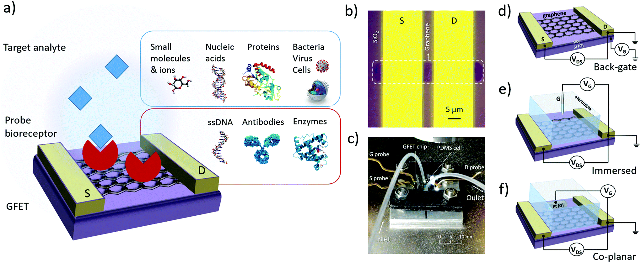 | ||
| Fig. 1 Design elements of a GFET bioanalytical sensor. (a) Typical layout of a GFET sensor, showing a graphene layer functionalized with biorecognition elements (red) and immersed in a media containing the target analyte (blue). (b) The graphene is connected with source (S) and drain (D) electrodes to generate electrical current along the atomically-thin layer. (c) Example of packaging with electrical connections to the electrodes and a flow cell with inlet/outlet for sample delivery. The gate (G) electrode, which modulates the electrical conductance of graphene, can be assembled in a (d) back-gate, (e) immersed or (f) co-planar configuration. | ||
2.1. Graphene material
Graphene is an atomically-thin material made of a two-dimensional hexagonal lattice of carbon atoms. This structure, with each carbon atom sharing three of its four electrons in covalent bonds with its nearest neighbors (sp2 bonds), is at the root of the robust mechanical properties of graphene.73 At the same time, the remaining fourth electrons are delocalized over the two-dimensional lattice in a Π orbital responsible for most of the material's optoelectronic properties.74 In the context of GFET sensors, we focus on the electrical and electrostatic properties of the material. Graphene is known for its extremely high mobility surpassing that of excellent metals.28,75 Being a semi-metal, its electrical conductance is moderately modulated by local electrostatic fields, allowing to operate the material in a field-effect transistor configuration. Because of this moderate ON–OFF modulation, graphene FETs are typically not considered competitive in pure electronics, compared to state-of-the-art 3D semiconductors such as silicon, or even to its 1D counterpart carbon nanotubes. However, their sensitive electrical conductance combined with their extremely high surface-to-bulk ratio provides them with significant advantages for chemical and biochemical sensing.Graphene can be produced by several different methods before integration in a FET device. First, graphene can be exfoliated from graphite, a material formed of multiple stacked atomic layers of graphene: the process consists in carefully extracting one monoatomic layer from the bulk graphite. Exfoliation can be achieved by various techniques, including chemical exfoliation,76 ball milling method,77 or more commonly micromechanical exfoliation, often referred as the “scotch-tape method”.77 The scotch tape method was the first reported to isolate graphene,28 and typically provides the best electrical properties, including the highest mobilities and least density of defects.78 However, it is difficult to obtain large-area flakes with exfoliation, which makes this approach less suitable for large-scale fabrication of devices.64 Graphene can also be grown by chemical vapor deposition (CVD), most commonly on metallic substrates like Cu or Ni.79 In this approach, a hydrocarbon precursor is introduced at high temperature, leading to graphene nucleation on the metal surface. Epitaxial growth on insulating SiC is also possible, in which case graphene nucleates following sublimation of the Si atoms.80 Graphene grown by CVD is often favored in recent works57,81 because it is practical to generate large-area graphene layers, making it the best candidate for scalable GFET production. On the other hand, the mobility may be lower than in mechanically exfoliated graphene82 and the transfer process following growth (see next section 2.2) can damage the graphene and leave impurities.83 Finally, another form of graphene is reduced graphene oxide (rGO), often used for its low cost and solution-processability.84 To produce rGO, a strong oxidation solution is used to separate graphite layers into suspended graphene oxide flakes, which are then chemically reduced back into graphene.85 The oxidation/reduction process tends to leave a high density of defects, which typically causes lower mobilities than in other types of graphene.86 Independently of the type of graphene used, most GFET sensor studies report working with a single layer of graphene. Some specifically confirm the presence of a single layer with Raman spectroscopy,65,83 as single-layer and few-layer graphene can be difficult to distinguish. Others use few-layers graphene,87 but single-layer has been reported to enhance the sensing performance.87
2.2. Substrate and electrodes
In order to form a GFET device, graphene must be transferred on a planar substrate that provides physical support to the thin nanomaterial as well as to the electrodes and sample delivery system. The substrate, or at least its top layer, is normally made of a dielectric or other insulating material to avoid unwanted electrical connections between the different electrodes placed on its surface. The most popular substrate for GFETs is degenerately-doped Si covered with a layer of SiO2 dielectric,49,56,61,88–90 which is common in the field of electronics and enables the use of the lower layer as a gate electrode (see Fig. 1d). However, SiO2 surfaces tend to trap charges and impurities, especially during the transfer process.66 Other materials are investigated as substrates, for example sapphire on which graphene can be grown directly, leading to enhanced mobilities.83 Research on more flexible and low-cost substrates is ongoing, for example with materials like flexible polyethylene terephthalate,48 silk fibroin91 or paper.92Multiple techniques are used to place graphene on its operating substrate, depending on the graphene source. Graphene flakes obtained by mechanical exfoliation can be directly transferred on the substrate from the adhesive tape used for extraction, by stamping the tape on the target substrate.93 This straightforward method provides clean, uncontaminated graphene, but is typically incompatible with large-scale FET production. Graphene growth by CVD is done on metal substrates,79 then the graphene is transferred onto a dielectric substrate using either wet or dry transfer methods. In wet transfer, graphene is protected on one side with a soft polymer layer, typically polymetylmetacrylate (PMMA), and the metal substrate on the other side is dissolved in an etching solution. The protected graphene is then rinsed and picked up onto the target substrate.94 Alternatively, protected graphene can be separated from the metal by electrochemical delamination.95,96 Dry transfer techniques include hot pressing and roll-to-roll methods based on thermal release tape (TRT) applied on the graphene.94 Pick-up and stamping with PDMS can also be used for dry transfer of graphene.97 In the case of rGO, the flakes can be transferred from solution onto the substrate of choice via a number of methods, such as drop-casting,43 dip coating98 or vacuum filtration on a membrane which is then stamped on the substrate.99 Graphene oxide flakes are either reduced before transfer, or first transferred and then reduced to rGO.
GFET design includes at least three electrodes, in order to operate as a field-effect transistor. The first two electrodes, called source (S) and drain (D), make direct contact with the graphene and enable the flow of electrical current in the graphene through the application of a difference of electrical potential between them (Fig. 1b). Source and drain electrodes are made of conductive material, typically a metal: most studies report using Au evaporated on top of a thin adhesion layer of Ti,87 Cr100 or Ni.101 Conductive silver paint can sometimes be used as the electrode material, especially on large area graphene.102 The third electrode, called the gate (G), is placed in close proximity to the graphene but not in direct contact. A potential difference is applied between the gate and the drain (or source) to modulate the density and polarity of charge carriers in the graphene; this mechanism is detailed in section 3.1 on electrical transfer curves.
Multiple configurations have been used for the shape and position of the gate electrode: these can be classified in three main categories illustrated in Fig. 1d–f. The choice of gate configuration depends on the experimental protocol selected for analyte delivery and detection. When the sensor is operated in air or other gaseous atmosphere, a back-gate configuration is usually favored (Fig. 1d). In this layout, the conductive lower layer of the substrate acts as the gate electrode, separated from the graphene and drain–source electrodes by a dielectric layer. Most often, this configuration is achieved using degenerately-doped silicon covered by a layer of thermal silicon oxide. The dielectric thickness determines the capacitance of the gate electrode, as discussed in section 3.1. In the case of SiO2, its thickness can be as large as the order of a micrometer, or as thin as approximately ∼10–100 nm, this lower bound being to limit the occurrence of pinholes between the backgate and graphene. However, in biosensing experiments, GFETs are most often directly operated in an electrolyte solution. In such configuration, the gate voltage is applied using either a reference electrode immersed in the medium (Fig. 1e) or a coplanar electrode patterned on the substrate (Fig. 1f). Reference electrodes made of Ag/AgCl represent a common choice since their use in electrolyte buffer is well calibrated.103 Others have reported immersed gate electrodes made of silver43,104,105 or platinum106 wires. Coplanar gate electrodes are patterned on the substrate in a similar approach as for source and drain electrodes, using deposition of metals such as platinum,55 silver107 or gold.48,108,109 In both cases, the gate electrode is coupled with the graphene via an electrical double layer formed by the redistribution of ions in the electrolyte medium;110 this is discussed in more depth in sections 3.1 and 4.1. These gate configurations are frequently referred to as “top-gate” or “liquid-gate”, but such terminology can be confused with solid-state planar electrodes placed on top of the graphene111 and with gating using an ionic liquid,112 respectively. For configurations described here as in Fig. 1e and f, we recommend using “electrolytic” or “electrochemical” to qualify the gate electrode.
2.3. Analyte media and delivery
Biological analytes (nucleic acids, proteins, ions, drugs) are normally found in physiological samples (blood, serum, plasma, urine), i.e. complex solutions containing multiple species as well as specific salinity and pH conditions. In calibration and detection experiments using bioanalytical GFETs, a variety of media types are reported, with different levels of similarity with actual physiological conditions. The choice of media also influences GFET sensitivity and signal strength, especially by its degree of screening of electrostatic charges: this property of the medium is characterized by the Debye length, which is discussed in more details in sections 3.1 and 4.1. In the following, we review different media types used in GFET experiments, as well as delivery methods used to expose the graphene surface to analyte-containing samples.The majority of reported GFET experiments are done in saline buffer, in which the purified target molecule is diluted at known concentrations.43,61,90,102,104 This approach allows to calibrate quantitation curves over a controlled range of analyte concentrations, and the saline environment is necessary to maintain the proper conformation of macromolecules (nucleic acids and proteins). However, high salinity environments create increased screening, which can make detection by GFETs more challenging (see section 4.1). In DNA detection, different saline buffers are reported; the most common is phosphate buffered saline (PBS) either at its physiologically-equivalent 1× ionic strength (137 mM NaCl, 2.7 mM KCl, 4.3 mM Na2HPO4, 1.47 mM KH2PO4),43,109 or diluted at 0.1×10⁴ or 0.01×.53,83 Lower salinity enables longer screening distances, allowing to detect hybridization in parts of the sequence furthest from graphene, but if the ionic concentration is too low (for example in water), strand repulsion can destabilize the double helix conformation.44 Other studies report using other buffers such as hybridization buffer (10 mM PB, 150 mM NaCl, 50 mM MgCl2),81 or 12.5 mM MgCl2 and 30 mM Tris buffer, known to be equivalent to PBS 1× for DNA helix stabilization.44,113 Protein detection experiments also commonly use PBS,61,89,102,114–116 and some groups have reported using 50 mM of PB117 or 5 mM MES buffer.64 Detection of E. coli bacteria was also shown in PBS buffer.84 For the detection of ionic species, target ions are generally diluted with or without competing ions, either in aqueous solution,118–120 HEPES buffer,39 Tris-HCl buffer,101,121 or PBS buffer.122
Some GFET experiments have reported the detection of analytes in more complex biological samples. For example, An et al.123 achieved the detection of mercury ions in real samples derived from mussels, and Wang et al.121 tested blood samples from children for lead ions. Thakur et al.46 detected the pathogen E. coli in river water samples. For proteins, Kim et al.115 captured the alpha-fetoprotein biomarker on the surface of GFETs by immersing directly in patient plasma, followed by electrical characterization in PBS after washing steps. Recently, Hajian et al.55 demonstrated DNA detection directly in genomic DNA extracted and purified from cell culture and in human genomic samples, whereas Ganguli et al.124 used loop-mediated isothermal amplification (LAMP) followed by detection of primer (ssDNA) on GFET sensors.
A few experiments completely evacuate the medium before electrical characterization. For example, Ping et al.65 exposed GFETs with solutions of DNA before drying and performing electrical measurements. Similarly, Islam et al.89 reported a back-gated GFET immunosensor for the detection of the human chorionic gonadotrophin (hCG) protein, in which the devices were exposed to probe and target in buffer solution followed by vacuum dry before characterization. In most experiments, however, measurements with GFETs are done directly in the analyte solution, which requires a method to contain the sample over graphene. The minimalist way to achieve this is by placing a droplet of sample on the GFET substrate to cover the graphene areas.125 Most often, a reaction cell is secured on the GFET substrate, enabling containment and delivery of the sample (e.g.Fig. 1c). Due to the small sensing area of GFETs, such cells are frequently made to contain low sample volumes of the order of tens of microliters.40,54,61,102,109 Because of their size, these are often referred to as microfluidic cells, although they do not necessarily use microscale flow control capabilities characteristic of microfluidic systems.126 Polydimethylsiloxane (PDMS) is one of the most popular materials for cell fabrication due to its chemical inertness, mechanical flexibility, transparency, easy processing and low cost.126,127 GFETs integrated with a PDMS cell have been used for the detection of various targets such as proteins,61,102,115 DNA,53,63,105,109 viruses47,48,128 and small molecules40,50 Other cell materials have been reported, for example poly(methyl methacrylate) (PMMA)53,83 and silicon rubber.90 The two most common cell designs used with GFET biosensors are the open cell and the flow cell: the first one consists of a simple top-open reservoir in which samples can be pipetted in and out.40,42,54,88,105,109,115,129 Flow cells generally consist of a small enclosed channel with tubing for sample inlet and outlet,50,53,61,63,64,130 allowing minimized evaporation and mixing between samples, lower sample volumes (few μL) as well as controlled fluid flow. This minimizes the consumption of reagents and samples, and lessens signal perturbations such as commonly observed during the loading/emptying of open cells.
In recent years, integration of GFETs into advanced microfluidic systems has been proposed to create versatile lab-on-a-chip miniaturized platforms. In particular, integration of GFETs in multichannel microfluidics enables multiplexing, i.e. the ability to parallelize the detection of multiple targets in the same sample. Several studies have demonstrated multiplexed GFET analysis for protein130 and DNA.53,63,109 Microfluidics integration can also enable GFET measurements under stable flow, instead of in static media. For example, Xu et al.53 quantified the kinetics and affinity of DNA hybridization using a high flow rate of 60 ml min−1 through the PMMA microfluidic channel. Similarly, Wang et al.61 presented a GFET integrated with a PDMS microfluidic flow cell to study the binding kinetics and thermodynamic properties of human immunoglobulin E (IgE) by means of time-resolved measurements performed under a flow rate of 5 μL min−1. Temperature-dependent binding kinetics measurements were possible due to the closed flow cell enabling minimal sample evaporation. Measurements in flow mode also ensured a steady concentration of analyte available for binding, thus decreasing detection times.53,60
2.4. Surface functionalization and passivation
GFETs can be used as sensors because the electrical conductance of graphene is sensitive to electrostatic changes in its environment; however the affinity between graphene and other molecules is not specific. For instance, graphene is known to interact with most proteins and nucleic acids, especially through hydrophobic domains of proteins131 and either the backbone132 or aromatic bases of nucleic acid.133 To engineer specificity in GFET sensors, it is necessary to functionalize the graphene surface with molecules able to specifically recognize and capture the target analyte; these biorecognition molecules are henceforward referred to as probe molecules. The coverage of graphene with probe molecules is often incomplete, in which case passivation strategies can be used to block non-specific interactions with graphene. In the following, we discuss the choice of probe molecules as well as strategies for probe immobilization and for passivation.For protein detection, the most common strategy is the use of antibodies as probes, due to their high specificity and affinity for their antigen. For instance, GFETs functionalized with antibodies have been used to detect proteins identified as cancer biomarkers: Kim et al.41 immobilized monoclonal antibodies against the prostate specific antigen (PSA) on a GFET biosensor, demonstrating highly sensitive detection of this biomarker of prostate cancer. In a similar way, monoclonal antibodies on GFETs were used to detect alpha-fetoprotein (AFP), a biomarker of hepatocellular carcinoma (HCC), in patient plasma.115 Other studies have used GFETs with antibody probes for biomarkers to other conditions, such as human Chorionic Gonadotrophin (hCG), a common pregnancy indicator.89 Antibodies on GFETs have also been shown to detect surface proteins of bacteria46,84,90 or viruses.47,48,136,137 For example, Chang et al.84 and Thakur et al.46 used anti-E. coli antibodies in order to detect the bacteria, and more recently Ono et al.90 used immunoglobulin G (IgG) to immobilize the gastric pathogen H. pylori on GFETs. Similarly, Liu et al.47 used specific antibodies to achieve rotavirus detection. Recently, GFETs with antibodies were also used to detect the SARS-CoV-2 virus responsible for COVID-19.136 Antibody probes were also used for the detection of larger complexes such as exosomes42 as well as small molecules such as the pesticide chlorpyrifos.56
Aptamers are another type of probe molecules used in GFETs; these are folded single-stranded DNA or RNA oligonucleotides that can bind a target protein or small molecule with high affinity and specificity. Saltzgaber et al.64 functionalized graphene with aptamers designed to bind specifically to human thrombin proteins. Farid et al.102 reported a GFET functionalized with aptamers for detection of the cytokine interferon-gamma (IFN-gamma) associated with tuberculosis susceptibility. Recently, Wang et al.61 studied the binding kinetics of human immunoglobulin E (IgE) to its specific aptamer, allowing the determination of thermodynamic properties of their interaction. In addition, the use of RNA aptamers has been reported for the detection of small molecules, such as the antibiotic tobramycin.50
The PBASE approach is also frequently used to immobilize proteins, by covalently reacting the succinimidyl ester group with the amine-terminated residue of an amino acid (e.g. lysine) available at the surface of the protein. For instance, this approach was successfully applied to immobilize various antibodies90,115 as well as the dCas9 enzyme used for detection in genomic DNA in Hajian et al.55 Some groups use biotin-streptavidin as an intermediary to immobilize protein probes:63,90 for example in Ono et al.,90 amine sites on the urease probes are functionalized with biotin linkers which are then coupled to streptavidin molecules immobilized on graphene with PBASE. A common aspect of these approaches with proteins is that there are frequently multiple available amine sites on a protein, and thus targeting these provides little control on the orientation of the probe on the sensor surface. This distribution can actually be an advantage for sensing by positioning part of the target-binding sites closer to the graphene surface below the screening limit (see section 4.1).141
Graphene can also be functionalized with covalent moieties, which can then be conjugated with biomolecules. A common reaction to do so is through the use of aryldiazonium salts, in which highly reactive radicals formed from reduced diazonium can directly bind to the carbon lattice of graphene.142 The functionality of the aryl group is chosen for further bioconjugation with biomolecule probes: for instance, 4-carboxybenzenediazonium tetrafluoroborate (CBDT) creates stable carboxyphenyl anchor groups on the graphene surface. These –COOH moieties can then be activated using EDC-NHS chemistry into a stabilized NHS-ester ready for coupling to an amine group on the probe, as described with PBASE above. Lerner et al.49 used this approach based on CBDT covalent functionalization followed by EDC-NHS reaction to immobilize an opioid receptor protein for naltrexone detection. Others have reported using the EDC-NHS reaction directly on carboxylated defects spontaneously present on the graphene material.117 In a reverse configuration, the functionalization of graphene with primary amines (–NH2) was shown using electron beam-generated plasmas produced in Ar/NH3; amine-terminated ssDNA were coupled with the amine-functionalized graphene using glutaraldehyde as a bifunctional linker.143
Covalent and non-covalent immobilization approaches have different impacts on GFET sensors. Covalent functionalization causes a significant structural change in graphene: it transforms the hybridization of carbon atoms at the functionalization site from sp2 to sp3. These point defects disrupt the conjugation of π electrons, and are known to alter the electronic properties of graphene, including its electrical conductance.144 However, covalent moieties are extremely stable on the graphene surface,142 which can be useful for sensors used repeatedly or with high flow rates. On the other hand, non-covalent functionalization such as PBASE does not alter the structural integrity of graphene and therefore its electrical properties.145 Hence, non-covalent functionalization, usually with PBASE, is largely favored for the immobilization of probe molecules on GFETs. Occasionally, some reports on GFET sensors use no graphene functionalization to immobilize the probes, for example by relying on non-specific interactions between DNA and the graphene.104,109 Other works have reported using metallic nanoparticles (such as Pt, Au) as intermediary between graphene and probes.46,107,146
![[thin space (1/6-em)]](https://www.rsc.org/images/entities/char_2009.gif) 46 or parylene.35 This protects the graphene and its electrical characteristics by preventing its direct contact with the sample media and the various molecules contained in it. Finally, GFET electrodes can also be passivated with dielectric films (e.g. SiO2/SiNx) either to block interaction with biomolecules and buffer solution, or to eliminate parasitic current.81
46 or parylene.35 This protects the graphene and its electrical characteristics by preventing its direct contact with the sample media and the various molecules contained in it. Finally, GFET electrodes can also be passivated with dielectric films (e.g. SiO2/SiNx) either to block interaction with biomolecules and buffer solution, or to eliminate parasitic current.81
3. Electrical measurements and metrics
FET-based sensors rely constitutively on electrical measurements, specifically measurements of the electrical current in the device channel – here the graphene layer (see Fig. 1). The general working principle of FET sensors is that the density of charge carriers in the channel (and hence the current) is modulated by the local electrostatic field, which is itself altered by physical or chemical changes in the environment around the channel. Alternate mechanisms to the field effect can include the generation of charge carriers (e.g. in photosensors) or changes in the scattering rates of charge carriers in the channel (e.g. due to increased disorder). In all cases, the detection principle of FET sensors is based on a change in electrical metrics induced by changes in the environment of the sensor. In FET biosensors, this principle is used to detect the capture of biomolecular species at the surface of the sensor. Graphene is a particularly good choice for FET sensors because its atomically-thin geometry makes its electrical conductance remarkably responsive to environmental effects, such as the capture or accumulation of biological analytes near the surface.In practice, the electrical current of FETs is also controlled by voltages applied to the source, drain and gate electrodes (see Fig. 1). The potential applied between source and drain generates the flow of charge carriers along the channel, while the gate voltage modulates the electric field across the channel – and thus the charge carrier density contributing to the current. FET devices are characterized using three standard curves: transfer curves (current vs. gate bias), output curves (current vs. drain–source bias) and time series (current vs. time) with fixed drain and gate voltages. In sensing applications, the effect of the analyte on such electrical curves can be monitored either a posteriori, by comparing a given metric before and after exposure to the sample, or in real-time by recording dynamic time series of the electrical current.
In this section, we examine specifically how GFET devices are electrically operated for bioanalytical sensing purposes. First, we review the characteristics of operating curves (transfer curves, output curves and time series) and the associated electrical metrics in GFETs. We then compare and discuss the use of these metrics for before–after or real-time detection of biological analytes.
3.1. Transfer curves
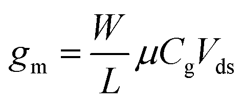
Transfer curves of transistors are obtained by sweeping the gate voltage Vg while maintaining a fixed bias Vds between the source and drain electrodes. The resulting current Ids (or resistance Rds = Vds/Ids, or conductance Gds = Ids/Vds) is plotted as a function of the gate bias. In GFETs, this plot typically results in a V-shaped curve, as illustrated in Fig. 2a. This shape translates an exchange in the polarity of the majority charge carriers in the graphene layer when sweeping the gate voltage: the left branch (or p-branch) represents an increasing density of positive charge carriers (holes), while the right branch (or n-branch) represents negative charge carriers (electrons). Between the two branches, the density of charge carriers – and thus the current – reaches a minimum with equal populations of both positive and negative carriers, referred to as the Dirac point or charge neutrality point (CNP). The p- and n-branches extend linearly from the charge neutrality point such that| Ids = gm (Vg − VCNP) | (1) |
 | (2) |
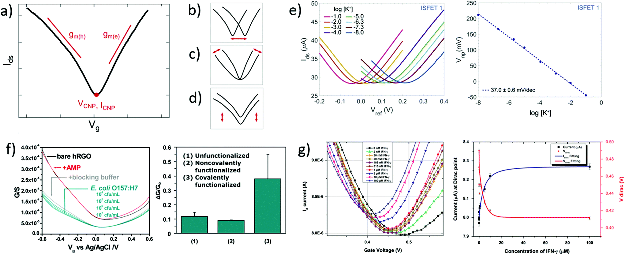 | ||
| Fig. 2 Transfer curves in GFET bionalytical sensors. (a) Typical transfer curve Ids (Vg) of a GFET, illustrating key metrics in its use as a sensor: (b) change in the voltage of the charge neutrality point VCNP, (c) change in the transconductance of electrons gm(e) or holes gm(h), and (d) change in the current amplitude, including at the charge neutrality point ICNP. (e) Left: GFET experiment showing a lateral shift of the transfer curve upon exposure to increasing concentrations of its target analyte, here potassium cations. Right: Corresponding shift of VCNP as a function of K+ concentration. Reprinted with permission from Fakih et al.119 © 2019 Elsevier B.V. (f) Left: Experiment with a GFET sensor for E. coli, showing a change of transconductance in the p-branch of the transfer curve upon increasing bacteria concentration. Right: Corresponding relative conductance change at fixed bias for different surface functionalization of the sensor. Adapted with permission from Chen et al.78 © 2014 American Chemical Society. (g) Left: GFET experiment for detecting interferon-gamma protein (IFN-γ), showing a change in all three metrics with exposure to the protein. Right: Response of VCNP and ICNP as function of IFN-γ concentration. Reprinted with permission from Farid et al.102 © 2015 Elsevier B.V. | ||
Transfer curves can be obtained using any of the three gate electrode configurations described in section 2.2 and illustrated in Fig. 1. The gate capacitance – and thus the transconductance – is highly dependent on this layout. In a back-gate configuration, the gate capacitance is dominated by that of the insulating layer separating graphene from the planar gate electrode, typically an oxide with a thickness t ranging from ∼10 nm to a few μm. The capacitance of this insulating layer is inversely proportional to its thickness: Cg ≈ Cox = εox/t, with εox the electric permeability of the dielectric. In the case of immersed or co-planar gate configurations, the shape and position of the gate electrode can vary considerably, but the capacitance is mostly determined by the electrical double layer (EDL) formed at the graphene surface by the reorganization of ions in the electrolyte media. This EDL acts similarly as a very thin dielectric layer – in the range of angstroms to a few nanometers.149 The resulting gate capacitance is much larger than that of back-gate dielectrics, and can reach levels comparable to the quantum capacitance CQ.150 The gate capacitance is then determined by combining the quantum and EDL capacitances in series: Cg = [Cq−1 + CEDL−1]−1.66 Gate potentials applied across the EDL can be over two orders of magnitude more efficient than through the back gate: consequently, the sweeping range of gate voltage required to capture the linear p- and n-branches is much smaller for immersed or coplanar gates, typically in the order of ±1 V,150 compared to ±10 V for thin oxides, going up to ±100 V for thick insulators in the back-gate. In electrolyte media, the range of gate bias sweep must also be restricted to avoid unwanted hydrolysis reactions and other electrochemically-driven reactions at the electrodes.66
The choice of gate configuration for a GFET sensor depends on the application. The capture of biomolecular analytes (nucleic acids and proteins) normally occurs during immersion of the probe-functionalized graphene layer in the sample, either an analyte-enriched buffer or a biological sample, such as biomedical (blood, serum, urine, etc.), food or environmental. Analyte detection by electrical measurements, though, can occur directly in the same media or after its removal. Immersed or co-planar gate configurations allow electrical measurements directly in electrolytic samples, and are thus usually favored in GFET bioanalytical experiments. The back-gate configuration is generally not used when the GFET interface is immersed with electrolytes, because screening by the EDL can lessen the back-gate voltage. Back-gated GFET sensors are more frequently used for the detection of volatile analytes in gaseous media, for example in applications such as the detection of pollutants.114,151 Nevertheless, back-gated GFETs have been recently reported to detect exosomes directly in buffer using the back-gate by exposing only part of the graphene surface to the sample,42 and they also have been used to detect DNA or naltrexone by immersing the device for exposure followed by drying before measurement.49,132 Drying the sample is limited to a posteriori detection and can result in non-specific adhesion of various species on the sensor surface, so particular attention to specificity should be exerted in this approach. Finally, let's note that the electrical interaction between analyte and graphene could also differ between dry and immersed conditions, as difference in environment are expected to alter screening effects as well as intramolecular charge transport properties.152
From transfer curves, several electrical metrics can be used for sensing, as illustrated in Fig. 2b–d and discussed in the following:
In biosensing experiments, the interaction between biological targets and biorecognition elements at the surface of graphene can alter the doping state of graphene, thus creating a shift in the CNP voltage from its initial value. This CNP shift is by far the most common metric for biosensing using GFETs.41,42,49 For example, Fakih et al.119 used the shift in CNP voltage as the sensing metric for K+ ions: they measured transfer curves for a wide range of concentrations of the target ion, as illustrated in Fig. 2e, showing a systematic shift of the curve with analyte concentration. In this experiment, the detection appears to be purely mediated by a doping mechanism, since the whole transfer curve is shifted without altering its amplitude and slope between measurements. From these transfer curves, a clear linear correlation between the CNP voltage and the log of analyte concentration was demonstrated, also shown in Fig. 2e. The change in VCNP is also used as a detection metric for complex macromolecular analytes such as DNA oligomers. For example, Gao et al.57 used the shift of the CNP as a sensing metric for 22 nt single-stranded DNA targets binding to hairpin DNA probes. They reported high sensitivity and specificity with this metric, using it to detect single nucleotide mismatches in the target. Finally, the change in CNP voltage is also frequently used to monitor intermediary steps in the assembly of the biorecognition layer, such as graphene chemistry or immobilization of biomolecular probes.46,57,104
The polarity of the CNP voltage shift raises interesting questions. Polarity represents the direction of the change on the voltage axis: p-doping when the CNP shifts to more positive voltage, n-doping when it shifts to more negative voltage. The polarity depends on the interaction between analyte molecules and the functionalized graphene layer. Polarities of the change in CNP voltage are reported in Table 1 for different types of analytes: cations, glucose and DNA. All cation sensors report a negative doping, which is consistent with an electrostatic gating model: the capture of positively-charged targets attracts negative charge carriers in the graphene, generating n-doping and a negative shift of the VCNP.66 Oppositely, negatively-charged target molecules would increase the density of holes in graphene and generate a positive shift. This electrostatic gating effect is usually postulated as the mechanism also involved in the detection of molecules; however observations are often inconsistent with this model. For instance, various experiments of GFET sensors for DNA and glucose present opposite polarities in the change of CNP voltage, as compiled in Table 1. For DNA sensors, this discrepancy is associated with at least two opposite effects. Studies observing a p-shift often attribute it to a chemical gating effect, in which the deprotonation of the phosphate backbone of the captured target DNA leaves it negatively charged in buffer, leading to the positive shift.58 On the other hand, observations of n-doping are explained by non-electrostatic stacking interactions between nucleotides and graphene,43,105 or donor effect,162 which is supported by DFT calculations.163,164. These differences may arise from experiment-specific differences in the graphene–analyte–solution interactions when immersed in electrolyte solution, including differences in DNA adsorption, DNA conformation and distribution of counter ions.165 In the case of glucose sensing, the mechanisms explaining the inconsistencies between experiments exposed in Table 1 have not been investigated in literature. The case of proteins is more complex, as their polarity changes with the pH of solution. In their work, Kim et al.41 observed the effect of pH on the VCNP shift for a PSA-ACT complex with an isoelectric point of 6.8: a negative shift of the VCNP was observed at pH 7.4 when the protein is negatively charged, and oppositely at pH 6.2 when the protein is positively charged. Considering that the density of proteins on graphene is typically too small to generate such a shift via direct charge transfer,166 the observed shift in VCNP was explained in this case by asymetrical scattering due to charged impurities.41 To summarize, the mechanisms behind the polarity of the VCNP shift seem to depend not only on the nature of the target, but also on design or environmental factors considering diverging responses reported from similar targets. Competing mechanisms have been suggested for DNA to explain those discrepancies and a mechanism has been suggested for proteins, but this topic calls for further investigation.
| Target | Doping polarity | Ref. |
|---|---|---|
| Cations (K+, Hg2+, Pb2+) | n− | 87, 101, 119–121, 155–158 |
| Glucose | p+ | 40, 91 and 92 |
| n− | 159 | |
| DNA | p+ | 57, 65, 81, 83 and 92 |
| n− | 43, 44, 59, 60, 63, 104, 105, 107, 109, 125 and 160–162 |
Using the change in transconductance directly as a metric requires a linear fit of the p/n branches; the required postprocessing for such analysis and the subjectivity involved in determining the lower and upper limits of the linear range can be considered as limitations of this method. Some groups use this metric indirectly by measuring the change in current at a fixed gate bias.78,170 This is robust in cases where the change of transconductance is the only observed variation. For example in Fig. 2f by Chen et al.,78 exposure to the analyte changes only the transconductance of the p-branch without affecting the CNP voltage; authors thus calibrated the current variation at Vg = −0.5 V against analyte concentration. In cases where the CNP voltage changes simultaneously to the transconductance, this indirect method would be problematic because it would then aggregate both variations, as discussed further in the following section. Finally, in other cases, the absence of change in the transconductance is explicitely reported and used to interpret the underlying mechanism of the biosensor. For example, Okamoto et al.88 observed positive doping without any variation in transconductance after the binding of negative antigen fragments, allowing them to hypothesize that antigen capture only changed the negative carrier density without introducing scattering effects.
3.2. Output curves
Apart from transfer curves, GFETs can be operated to measure output curves, in which the drain–source current Ids is recorded as a function of drain–source voltage Vds for a fixed gate voltage Vg. The typical output curve of a GFET is represented in Fig. 3a: as the applied bias increases from zero, the amplitude of the current increases with the same polarity as the applied bias. The curvature of the output curve is generally considered a good indicator of the quality of the contacts between graphene and source/drain electrodes, and of charge transport along the graphene. With good graphene and electrical contacts, a linear ohmic regime is usually expected at low bias.171,172 In practice though, a positive curvature or superlinear regime is sometimes observed due to potential barriers created by non-ideal contacts or defect sites.147 The output conductance gds is defined as the slope of the output curve. Its amplitude is evidently function of the gate voltage, which modifies the carrier density, as seen in Tsang et al.42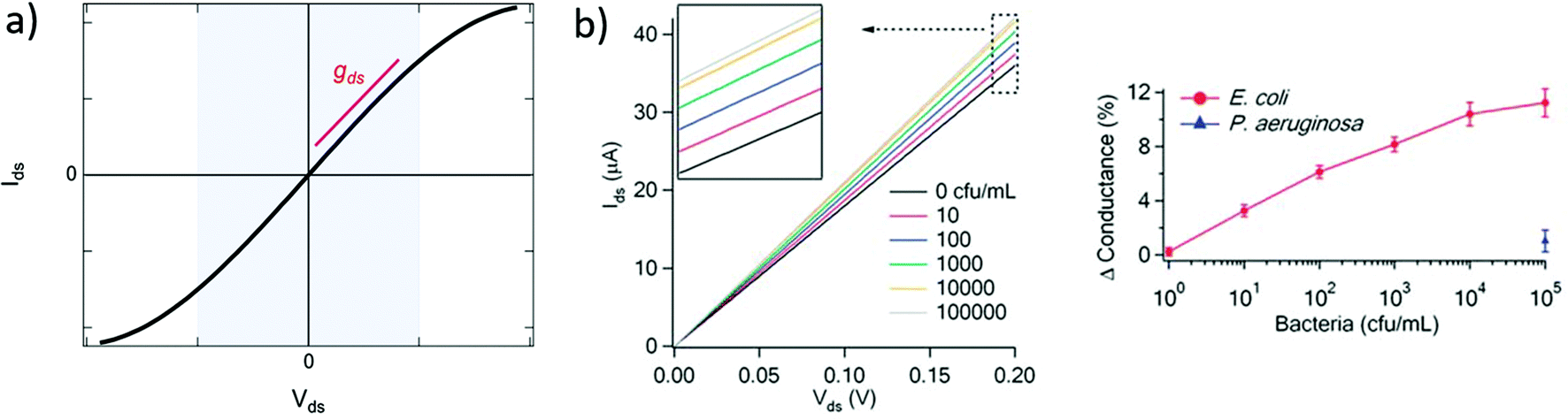 | ||
| Fig. 3 Output curves in GFET biosensors. (a) Typical output curve Ids (Vds) of a GFET: the shaded area indicates the low-bias regime, expected linear, which slope corresponds to the output conductance gds. (b) Left: Experiment with a GFET functionalized with E. coli antibodies, showing a change in output conductance after incubation with the bacteria. Right: Corresponding change in the relative conductance as a function of E. coli concentration. Reprinted with permission from Huang et al.45 © 2011 The Royal Society of Chemistry. | ||
A change in the output conductance is occasionally used as a detection metric in GFET sensing experiments. For example, this is done by Huang et al.45 in Fig. 3b: on the left, they show output curves taken at Vg = 0 V after a fixed incubation time in increasing concentrations of bacteria. On the right, the variation in current at Vds = 100 mV is used for quantitation of the bacteria. The increase in output conductance with increasing concentrations suggests either p-doping or an increase of the transconductance (decrease of disorder). To disambiguate between the two, transfer curves were acquired at concentrations 0 cfu mL−1 and 100 cfu mL−1, showing a p-shift and no transconductance change. This allowed the authors to attribute the variation of output curves to an increase of negative carriers in the system, due to the negatively charged bacteria through electrochemical gating. As this example demonstrates, output curves as a sensing metric should be paired with at least a pair of transfer curves in order to distinguish a change in carrier concentration from a change in disorder.
3.3. Time series
In time series, the evolution of the drain–source current (or conductance, or resistance) is collected as a function of time at fixed drain–source and gate voltages. Time series typically start recording before the introduction of reagents and follow the evolution of biochemical interactions between analyte and sensor. These interactions induce variations in current as a function of time, due to changes in charge carrier concentration or scattering effects via mechanisms discussed in earlier sections. Detection of the analyte, and sometimes its quantitation, is assessed from the change in electrical current after injection of the analyzed sample. Since the gate voltage is fixed, this curve is akin to following the evolution of a single point of the transfer curve in time. The choice of gate voltage has a direct influence on the amplitude and the polarity of the signal. It is generally expected for the signal amplitude to be maximized when choosing a gate voltage corresponding to a high transconductance region of the transfer curve.64 Actually, the interplay between gate voltage and signal amplitude can be quite complex, as illustrated in subsets a to e of Fig. 4. Subset a represents a system undergoing a p-doping shift between times t1 and t2, and subsets c to e schematize the resulting times series taken at three different gate voltages (VA, VB and VC). Even though they result from the same analyte–sensor interaction, time series obtained at gate voltages VA, VB and VC exhibit current changes of different amplitudes (ΔIA > ΔIB) or even different polarities (ΔIB < 0 and ΔIC > 0). We see here how a slight change of gate voltage, especially close to the CNP, can result in a significantly different profile of the time series. This was experimentally demonstrated by Sudibya et al.,38 who observed both an increase and a decrease of current with increasing concentration of Ca2+ ions, depending on the chosen Vg. These results highlight the fact that a variation in electrical current cannot be associated to a specific doping polarity without characterization of the transfer curve profiles before and after interaction with the analyte. Moreover, current variation in time series cannot be interpreted as a specific mechanism by itself: for example, the time series represented in Fig. 4d could equivalently be generated by p-doping (Fig. 4a at VB) or by a decrease of transconductance in the p-branch (Fig. 4b at VB). Insight from transfer curves is thus also necessary in order to correctly identify the mechanism generating current variations in time series.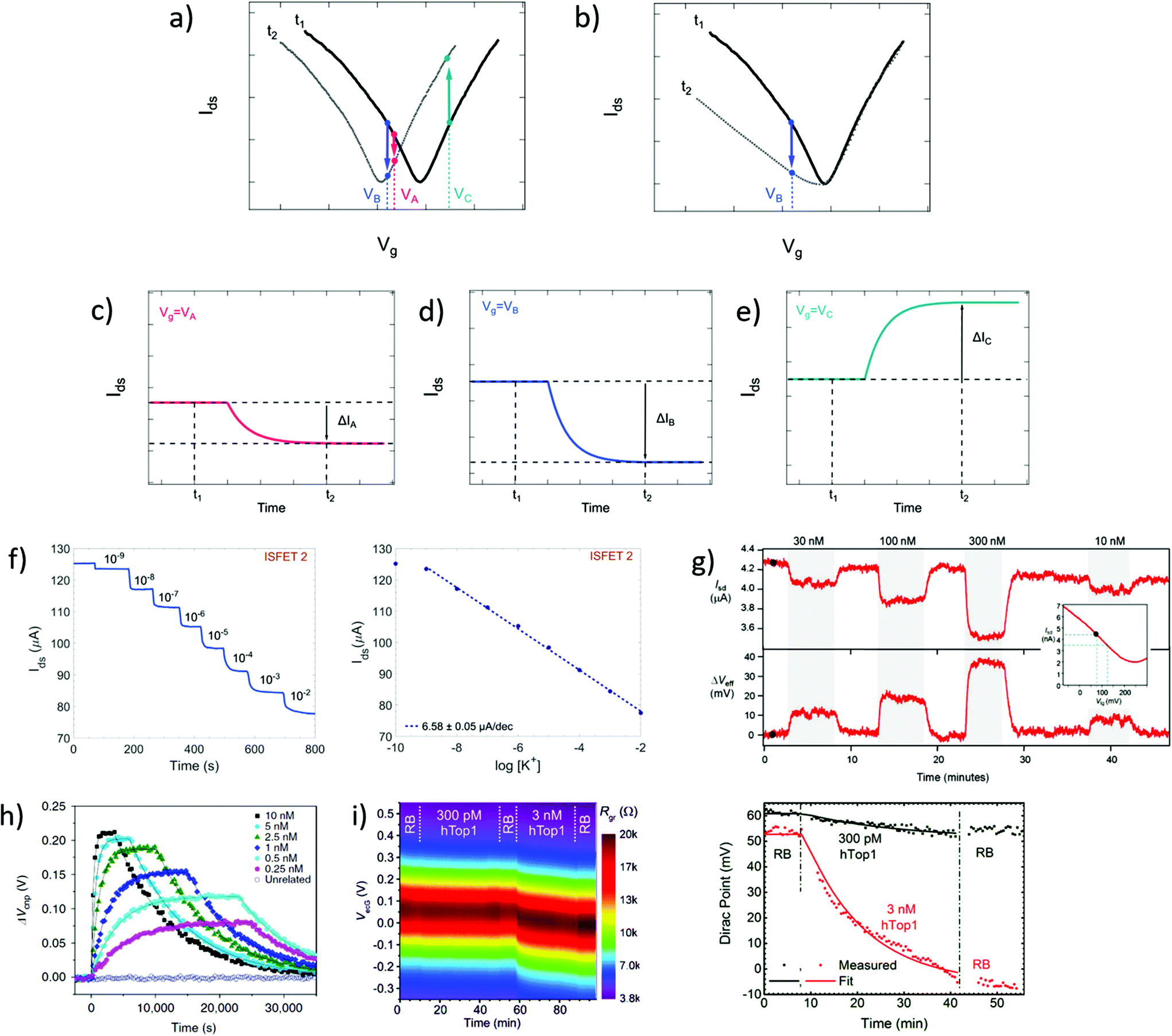 | ||
| Fig. 4 Time series in GFET biosensors. (a) GFET sensor detecting a left-shift of the CNP voltage, captured in two transfer curves at time points t1 and t2. (b) Same for a system undergoing a change in p-branch transconductance. (c)–(e) Corresponding time series of current I(t) at specific gate voltages VA, VB and VC. (f) Left: Time series of current in a GFET sensor for K+ ions, recording the exposure to increasing concentrations of analyte. Right: Corresponding change in current as function of K+ concentration. Reprinted with permission from Fakih et al.119 © 2019 Elsevier B.V. (g) Time series of a GFET sensor for thrombin, recording the introduction of various concentration of analyte separated by washing cycles. Top series shows the current as a function of time, and bottom series the corresponding change in CNP voltage using the conversion described in the inset. Reprinted with permission from Saltzgaber et al.64 © 2013 IOP Publishing, Ltd. (h) Time series of the change in CNP voltage, also obtained by conversion, showing hybridization and dissociation kinetics between ssDNA probes immobilized on a GFET and different concentrations of the complementary ssDNA. Reprinted with permission from Xu et al.53 © 2017 Springer Nature. (i) Left: Two-dimensional time series showing electrical current as a function of both gate voltage and time, here for a GFET sensor targeting the hTop1 enzyme. Right: Time series of the CNP voltage, extracted from the 2D plot, during introduction of hTop1 at two concentrations (right). Reprinted with permission from Zuccaro et al.54 © 2015 American Chemical Society. | ||
Time series most often directly present the value of the current as a function of time, as in experiments of Fakih et al.119 in Fig. 4f and of Saltzgaber et al.64 in Fig. 4g (top part). Sometimes, the current is converted as a change in voltage such as in Saltzgaber et al.64 in Fig. 4g (bottom part). An effective voltage shift representation was also used by Xu et al.53 to study the kinetics of DNA hybridization events and extract binding constants for several concentrations of target (Fig. 4h). In this approach, the current change ΔIds is converted to a voltage change with the relation ΔVCNP = ΔIds/gm. It's important to note that this approach is only valid if the transconductance remains constant before and after the addition of targets. As previously mentioned, transfer curves should be provided to confirm that doping is the only mechanism at play. Signal in time series is sometimes normalized as a relative change from a baseline current. Use of normalization can help in assessing signal strength despite sensor-to-sensor variations and effects associated to the medium.55 For example, Chen et al.50 used a simple normalization Ids/I0 with I0 the initial current in deionized water and Liu et al.47 showed a relative current (Ids − I0)/I0 with I0 the stabilized current after immobilization of the probe molecules. When normalized signal is presented, the conditions used for the baseline should be specified and it is good practice to make available the original time series of the baseline and of the experiment before normalization.
It is possible to avoid the limitations of time series following a constant gate voltage, by implementing a more sophisticated acquisition protocol based on an oscillating gate voltage. In this approach, the gate voltage is continuously swept back and forth over a defined range while the drain–source current is recorded. This results in a two-dimensional mapping of the electrical current as a function of both gate voltage and time. Ideally, the range of the gate voltage sweep is chosen to cover the CNP, which allows to follow the doping state of the graphene at each time point. For example, Zuccaro et al.54 applied this approach of continuous gate sweeps to produce 2D maps of the low-bias resistance as a function of gate voltage and time, as shown in Fig. 4i (left). This approach allows to extract a time series of the VCNP, as illustrated in Fig. 4i (right), which is a powerful way to quantify the kinetics of the change in doping state.
3.4. Comparison of electrical metrics in “before–after” vs. “real-time” protocols
An important consideration when designing a biosensing experiment with GFET sensors is deciding which type of electrical measurements and metrics to use, and in which sequence to collect them. The design of the acquisition protocol depends on the nature of the scientific question or application for which the biosensor is used. We can divide protocols into two categories: “before–after” and “real-time”. The former refers to experiments comparing the value of a metric, at a specific time point after exposure to the sample, to its baseline value before exposure. This is suitable if the goal is to assess the presence of a target (yes/no type of result). It is also relevant for applications requiring quantification of an analyte: the amplitude of the change in the chosen metric is then compared to a previous calibration of the sensor. However if the application or the scientific question requires information about the kinetics of the biochemical interaction, then a “real-time” protocol recording the evolution of a metric over a relevant period of time is necessary. Among the previously described metrics, some focus on the state of the system at a specific time point, while others allow to monitor the evolution of the system, which makes them naturally more or less convenient for each protocol type.Transfer curves are especially suitable for before–after measurements, as they provide an informative picture of the electronic state of the sensor at a fixed point in time. Indeed, this type of curve provides information on the doping level, through the CNP position, as well as on both carrier mobilities (electrons and holes), through the transconductance of each branch. Transfer curves can be used to assess completion of different steps of sensor assembly, functionalization and biochemical interactions, by collecting a gate sweep after each step and comparing the resulting electrical metrics to the initial curve. Even in experiments focused on real-time measurements for reaction kinetics, it is recommended to collect at least initial transfer curves to assess the performance of the sensors, as done by Cohen-Karni et al.173 In general, before–after analysis of transfer curves is useful for events that have clear before and after states, which are typically before exposure to a reagent and after the reaction with this reagent is considered completed. This type of measurements is commonly used to verify the impact of a passivation layer,46 to confirm the presence of functionalization adducts,57 to assess the linking of the probes121 or the linking of the target to the probes.44 In sensing experiments, this method is most frequently used for quantitation with various types of analytes including ions,121,122,158 proteins,102,130 glucose40,159 and DNA.63,65,83 It is also used for simple yes/no detection, like to assess the presence of a single-mismatched DNA43,44,57 or a specific ion.158 Output curves can be used in the same way as transfer curves in before–after detection schemes, such as in Huang et al.,45 but they provide less information on the electrostatic state of the graphene and on physical mechanisms occurring in the system (e.g. change in doping or diffusion). The analysis of transfer or output curves usually requires post-processing, because the extraction of the CNP voltage, transconductances or output conductance can be performed only after completion of the relevant voltage sweep. From the transfer curve, the CNP voltage is often estimated using the point of the transfer curve with the minimum of current.133 Other studies use curve-fitting to extract the voltage associated with the minimum, usually with a quadratic function63 or with more sophisticated models.65 Curve fitting is a more precise method since it is not limited by the width of the gate voltage steps during the measurement. The postprocessing required to determine the transconductance of each branch (gh and ge) involves subjectivity in determining the lower and upper limits of the linear range, which can be considered a limitation of this method. Real-time measurements are usually performed via unidimensional or bidimensional time series as described in section 3.3. Real-time measurements are of course essential to study the kinetics of a dynamical reaction.40,53–55,88,174 In such experiments, like the study of DNA hybridization by Xu et al.53 illustrated in Fig. 4h, the electrical current is monitored during the introduction of analytes and during washing steps. Time series covering washing steps enable to monitor either the removal of non-specific species and unbound analytes or, in the case of weak probes:target affinities, to observe the dissociation of the analyte from the sensor. Time series can be adjusted with a Langmuir binding kinetics model or similar model to estimate adsorption and dissociation constants.53,108 Time-resolved measurements can also be used for quantification purposes. For example, Fakih et al.119 studied the influence of K+ concentration with both transfer curves (Fig. 2e) and time series (Fig. 4f), and observed similar correlations with analyte concentration. This type of experiment is especially conclusive when the signal reaches a clean plateau during target exposure, like in Fig. 4f: such stabilization of the signal facilitated its quantification, which is critical for analyte quantitation. A combination of the two purposes, kinetics and quantification, can be done simultaneously, like in Saltzgaber et al.64 in Fig. 4g, where the successive introductions of different target concentrations, separated by washing steps, are analyzed to gain insight on the effect of concentration on the kinetics of the reaction. Real-time experiments also allow to assess the reaction rate and the time required to stabilize the interaction between the analyte and the target, which can then be used to determine how to time transfer curves for before–after measurements. For real-time biosensing, experiments need to be done in a saline environment with a coplanar or immersed gate configuration, which requires a flow cell or microfluidic circuitry. Measurements can be done in a static or continuous flow setting. Faster reaction times have been reported for DNA sensing in such settings,53,134 but continuous flow was reported to lead to noisier signals because of vibrations due to the water pump.50 The choice of flow configuration thus depends on the priorities in the experiment.
For most experiment purposes, both types of measurements are best used together. Standard time series are very instructive about the kinetics of the analyte–sensor interactions, but since they only measure the current at fixed biases, they provide little insight on the physical mechanism underlying these interactions. When time series are coupled with transfer curves, either at specific time points or, even better, continuously in two-dimensional time series,54 then the mechanisms behind the evolution of the current can be further investigated. In addition, quantitative analyses based on current changes (either for quantitation or kinetics) often rely on the assumption that the change in current is proportional to the change in graphene doping state, but this is only true in the linear regime of p/n branches and if there is no change of the charge carrier mobilities during the reaction; this needs to be confirmed with transfer curves. Finally, when using before–after experiments without any time series, it is difficult to assess whether the interaction with analytes is stabilized or not; consequently, incubation times are often chosen very long in order to make sure the reaction has occurred. The use of time series, at least during calibration assays, could help optimize the incubation time used in detection assays.
4. Performance assessment
The experiments considered in the scope of this review aim at developing GFETs as a bioanalytical technology, i.e. for the detection or quantitation of molecules relevant in biology. In this section, we review the criteria used to evaluate the performance of GFETs as biosensors. In this context, performance include two aspects: quality and reliability.175 Quality criteria are established by the performance of the sensor itself with respect to several detection metrics. In the following, we discuss four of these metrics: spatial range of detection, limit of detection, sensitivity to target concentration and response time. Reliability criteria can be assessed by the experimental design; here we will discuss appropriate statistical sampling and analysis, as well as controls experiments.4.1. Spatial range of detection
For electrolyte-gated GFETs, it is important to take into account charge screening by mobile ions in the medium. According to the Debye–Hückel model, charged molecules in solution are screened by mobile counter-ions such that their electric potential is dampen exponentially with distance, with a decay constant λD called the Debye length. This constant represents the screening length and is given by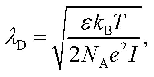 | (3) |
 where ρi and zi are respectively the density and valence of ion species i. Generally speaking, the Debye length represents the distance at which charges are screened; thus, charges located farther than the Debye length are usually considered out of range for electrostatic detection by a FET sensor.176–178 For an aqueous solution at room temperature, this length becomes
  where I is in mol L−1. For 1× PBS buffer, it is as short as ∼0.7 nm. Therefore, one must take λD into consideration when designing specific probe molecules, as too-long a distance between target binding events and the FET surface may significantly reduce the signal146,178–180 or completely screen it out.146,176 Such limitations due to Debye length on the spatial range of detection in FET sensors have been experimentally observed in different types of FETs. For example, Sorgenfrei et al.178 used an ssDNA probe tethered to a CNTFET to study the effects of shortening the Debye length, via changing PBS concentration, on the detection of probe hybridization with a target complementary DNA (cDNA). They found the resistance to decrease significantly (resistance change ΔR/R dropping from 80% to 10%) when increasing buffer salinity from 0.1× to 5× PBS (corresponding to a decrease of λD from 2.3 nm to 0.3 nm). They also showed that moving the target cDNA further from the surface, by removing two base pairs from the target cDNA (∼0.66 nm distance increase), reduced ΔR/R ∼ from 80% to 20%. This was performed in 1× PBS and, notably, a signal was still detectable, although greatly reduced, even though hybridization occurred at distance of ∼1.36 nm, exceeding the estimated λD of 0.7 nm.
This proximity requirement between the captured analyte and graphene presents a challenge in designing the interface of GFETs, especially in biomedical applications targeting detection in physiological samples. Saline buffers such as 1× PBS or 1× PB, commonly used to emulate physiological environments (e.g. human blood), have a very short Debye length of 0.7 nm. In comparison, common probe molecules such as antibodies for protein detection can be upwards of 10 nm in size. To circumvent this issue, some groups have opted to use solutions with low ionic concentration in order to achieve λD above 10 nm.41,64,181 Others have designed smaller probe molecules such as antibody fragments88,182 or aptamers,61,146,183,184 allowing to reduce probe length from 10–15 nm to <5 nm, in order to improve device sensitivity. For instance, Kim et al.146 found that replacing a typical antibody probe (∼10 nm) with an aptamer probe (∼4 nm) on otherwise similar GFET sensors improved sensitivity to the target protective antigen (PA) by 1000 times (12 aM to 12 fM) in 10 μM PBS (λD ∼ 23.6 nm). They also found that signal of PA binding was completely screened out in 1 mM PBS (λD ∼ 2.3 nm), even using small aptamer probes, whereas using 10 μM and 100 μM PBS (7.3 nm and 23.6 nm, respectively) showed similar signal intensity (determined by the shift in the charge neutrality point) and limit of detection (smallest concentration detected). Interestingly, the range of PA concentration covered before reaching signal saturation was narrower in 100 μM PBS, indicating lower salt concentration solutions to yield a wider range of detection.
In the case of DNA hybridization experiments, however, many groups have reported detection at very high salt concentrations43,81,104 and even for very long DNA sequences.44 This reduced limitation to the screening length is likely enabled by the capture of charges close to the FET surface by the first nucleotides of the probe DNA, regardless of its total length. Although high salt concentrations are preferred for stabilizing double-strand DNA, signal and sensitivity can still be improved by decreasing salt concentrations.44,53,63,104 Additionally, single nucleotide polymorphism have been detected,43,53,81,125 even if located further along the DNA strand than the Debye length. This is explained by the decreased hybridization stability of single mismatched DNA,43,81 leading to partial or complete dissociation of the duplex near the graphene surface.
Many strategies for overcoming Debye length limitations while maintaining physiological environmental conditions have been proposed: such as displacing the screening range away from graphene by covering it with a polymer layer permeable to biomolecules185 or with charged macromolecules to create a fixed-ion region.55,186 Similarly, Chen et al. reported extending the screening length by adding an MoS2 layer on graphene.162 Other strategies include indirect detection of a target via the products of its reaction on an enzyme, produced outside of the screening length and diffused to the surface of the GFET90 and using a solution containing 12.5 mM of MgCl2 in a 30 mM Tris buffer, known to provide similar dsDNA stability as in 1× PBS, to increase λD to 1.6 nm.44 Finally, issues related to electrolyte screening can be circumvented all together using a backgate and measuring in air conditions.89
4.2. Limit of detection and sensitivity
The performance of GFETs as biological transducers is commonly referred to as their sensitivity.43,56,125 Formally, analytical sensitivity describes the ability of the sensor to distinguish between small differences of analyte concentration.187 Interestingly, this property is actually rarely assessed in bioanalytical GFET studies; rather, the most widely reported performance metric is the limit of detection (LOD),41,48,58,81 which indicates the lowest concentration at which an analyte can be confidently detected by the sensor. Both of these metrics, sensitivity and LOD, are often conflated, yet they represent distinct standards.Sensitivity is a crucial performance metric for quantitation applications, in particular when it's required to identify analyte concentration with great precision. Sensitivity can be assessed from the calibration curve of the sensor, i.e. the evolution of a chosen electrical metric (ex. CNP voltage, current, see section 3) as function of analyte concentration, as illustrated in Fig. 5a. Sensitivity is generally quantified as the slope S of the linear regime of the curve, given by
 | (4) |
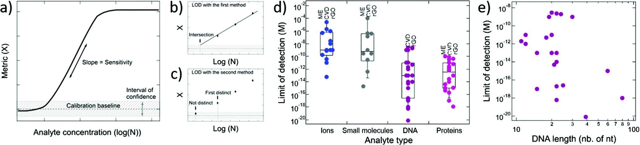 | ||
| Fig. 5 Sensitivity and limit of detection (LOD) in GFET biosensors. (a) Typical calibration curve for a GFET sensor, showing the change in a given electrical metric as a function of analyte concentration. Sensitivity represents the slope of the linear regime, while the LOD is the concentration at which the change in the metric exceeds a chosen confidence interval. (b–c) Methods for the experimental determination of the LOD based on extrapolation and direct measurement, respectively. (d) LODs reported in the literature for GFETs, classified by analyte type: ions, small molecules, DNA and proteins. Data points are also separated as function of the type of graphene used in GFET fabrication (ME = mechanical exfoliation, CVD = chemical vapor deposition, rGO = reduced graphene oxide). (e) Reported LODs for DNA detection represented as function of the length of the targeted DNA sequence. | ||
The limit of detection is a different important performance metric, that determines the minimal concentration of analyte detectable by the sensor. The LOD is determined as the concentration at which signal exceeds the baseline by an interval of confidence, as illustrated in Fig. 5a. A low LOD depends positively on signal strength and is limited by noise and other sources of variance in the measurements. Although distinct, the LOD and sensitivity can be correlated. For instance, in Fig. 5a, we can see that improving the sensitivity or the slope in the calibration curve is likely to lower the LOD. The LOD is relevant for detection and also for quantitation of analytes: it determines the lower bound of the dynamic range of the sensor, the upper end being limited by the saturation of the signal. In practice, the required LOD depends on the purpose of the sensor: for some applications, a predefined LOD needs to be achieved as prescribed by norms or regulations, for example safe Pb2+ levels in children's blood121 or glucose levels associated with diabetes.159 In the development of GFET biosensors, the LOD is the most frequently reported indicator of performance, and is often benchmarked against other detection techniques, such as PCR-based techniques for DNA detection,81 or ELISA tests for immunoassays.174 We surveyed the literature on GFETs used as bioanalytical sensors and retrieved 61 studies reporting a value for the LOD (see the ESI† for a list of the studies). An interesting observation from that compilation is that the reported LODs cover a very wide range of concentrations, from 0.1 mM (ref. 91) to 8 zM,124 which represents a remarkable spread of 16 orders of magnitude. In the following, we discuss the different factors that can influence the LOD in GFETs.
First, we note that methodologies to determine the LOD vary between studies. They can usually be classified in one of two categories: extrapolation53,134,189,190 or direct measurement,41,49,65,89,120,121,174 illustrated in Fig. 5b and c respectively. Both approaches first require precise characterization of the sensor baseline, i.e. the value and standard deviation of the chosen electrical metric (ex. CNP voltage, current) in absence of the targeted analyte. The LOD differs from the baseline of the sensor by an interval of confidence, defined as a chosen multiple of the standard deviation. The International Union of Pure and Applied Chemistry defines the LOD to be at three times the standard deviation,191 and the number of replicas for baseline measurement is recommended at n = 20.192 In the first approach, the electrical metric is measured in presence of different concentrations of analyte, and the resulting response is extrapolated towards lower concentrations. The LOD is then identified as the concentration value at which the extrapolation function intersects with the upper bound of the interval of confidence. For example, Chen et al.50 used a linear fit to extract a correlation between the relative current change observed in time series and the logarithm of analyte concentration. From data taken in a range of 10 nM to 100 μM, they extrapolated this linear fit until reaching a signal-to-noise ratio of 3, and obtained an LOD value of 0.3 nM. More complex non-linear fits can be used as well for extrapolation, such as a Hill-Langmuir equation as used by Li et al.39 The second approach consists in actually making measurements at decreasing concentrations, with replicas, until the observed change in the electrical metric is no longer statistically different from the interval of confidence. For instance, Cai et al.43 measured the sensor response for concentrations down to 10 fM of complementary DNA. However, after assessing the noise level with a blank control test, the LOD was established at 100 fM, corresponding to a signal exceeding three times the background level. This underlines the importance of assessing the baseline value and its variance. In some specific cases, it is more relevant to use another threshold than the baseline signal to determine the LOD. For example, in Campos et al.,81 the LOD of perfectly-matched DNA is determined as the concentration sharing the same signal value as the highest signal obtained with single-mismatched DNA. In general, the LOD assessment method should be detailed in order to enable proper benchmarking between studies. In our literature survey (see ESI†), the LOD values were taken as reported, without adjustment for the determination method. Extrapolation methods tend to require less measurements, but the extracted LOD can be off the mark if analyte signal deviates from the extrapolation model at low concentrations. In this case the second type of approach is the most reliable as it ensures that concentrations above the LOD can really be distinguished from the baseline. When used properly, i.e. with robust statistical analysis and with the right extrapolation function, the two methods should provide equivalent results for the LOD. In studies, the lower concentrations measured and the extrapolated values vary by usually less than an order of magnitude53,134 and at most, by two.159 The data may also include underestimations of the LOD, if the interval of confidence associated with the variance of the baseline is not properly assessed. All things considered, we estimate that discrepancies from the LOD evaluation methods add some variance to the dataset, but are not sufficient to explain the wide spread of LODs across all experiments.
To analyze the distribution of LODs in the literature, we first classified the data by type of analyte, namely ions, small molecules, DNA and proteins. Fig. 5d compiles individual data points and the corresponding box plots characterizing their distribution for each type of analyte. Interestingly, we observe differences in the distributions with analyte type. Ions sensors show the most compact distribution, with a geometric mean and standard deviation of the LOD = 10(−8.5±2.3) M (n = 14). This is consistent with ions being the most homogeneous category, almost entirely consisting of monoatomic species. Small molecules present a distribution of 10(−8.9±3.2) M (n = 10), which is not significantly different from that of ions (p-value = 0.7 for a two-tailed two-sample Student's t-test assuming non-equal variances). The variance for small molecules is larger than for ions, which may reflect a higher heterogeneity in this category regrouping glucose and various other organic molecules. We note that the charge of the analyte does not appear as a dominant factor in determining the LOD of GFETs: ions present a net charge whereas small molecules don't – yet they present similar LOD averages. On the other hand, nucleic acids and proteins present LOD distributions with much lower averages, respectively 10(−13.2±3.4) M (n = 23) and 10(−13.1±2.4) M (n = 20). These distributions are very similar to each other, and both significantly different from that of ions (p < 1 × 10⁻⁴ and p < 1 × 10⁻⁵, respectively). It appears that there is a distinct segregation between small species (ions, small molecules) and large macromolecules (DNA, proteins). This is likely due to the size difference: macromolecules contain hundreds to thousands of atoms arranged in complex higher-order tri-dimensional structures. Consequently, they are individually more perturbative of the electrostatic environment near the GFET graphene layer, either by carrying more charged sites, by covering a larger area on the graphene and/or by displacing their volume in the saline media. In the same direction, the few GFET studies on the detection of cell-sized analytes such as bacteria and viruses also tend to report very low LODs for these very large analytes.46–48
Within macromolecules, the size of analytes can also vary significantly, depending on the length of the DNA sequence or the mass of the protein. Size effects at this scale have been reported in other techniques, for instance improved detection metrics with longer DNA sequences in surface plasmon resonance193 or DNA microarrays.194 In the GFET literature, we looked for a distribution of LODs with size in macromolecules, but observed no significant trend in the available data. For instance, Fig. 5e maps the reported LODs of the 23 DNA studies as function of the length of the target sequence, which reveals no observable correlation. We obtained a similar scattering with protein data points as a function of protein mass (not shown). This suggests that eventual size effects within macromolecules, if they exist, are not dominant compared to variations in sensor and experimental design between studies (discussed below). It should be noted that a series of studies from the Johnson group, using a consistent GFET design, reported lower LODs when increasing the length of the DNA oligomer.57,58,65 In this specific set of experiments, GFETs were rinsed and dried after immersion in the DNA solution, so that detection was performed using back-gated transfer curves. In contrast, most GFET DNA studies use electrolyte-gated designs, in which detection is limited by Debye screening and thus dominated by nucleotides tethered near the graphene surface. This could explain the lack of dependence with DNA length observed overall in the literature data.
Once classified by the type of analyte, LOD values in the literature data still spread over 8 to 12 orders of magnitude per analyte type; this remaining variance must come from differences between studies in the design of GFET sensors (e.g. materials, geometry, surface chemistry, etc.). In particular, it is often suggested that the quality of the graphene is important to produce an efficient FET sensor.49,83,123,125 The underlying rationale is that LOD is limited by noise, and that high-quality graphene presents higher mobilities and lower noise spectral density.188 We looked into the type of graphene used in GFET assembly (exfoliated, CVD or rGO) as a proxy for graphene quality: it is commonly expected for mechanically exfoliated graphene to present high mobility, and for rGO to present a high density of detects, due to their respective fabrication and transfer methods (see sections 2.1 and 2.2). In the data we collected from the literature, reported mobilities for exfoliated graphene are between 200 cm2 (V s)−1 (ref. 90) and 4400 cm2 (V s)−1,195 and in a similar range for CVD from 605 cm2 (V s)−1 (ref. 125) to 5000 cm2 (V s)−1.119 For rGO, they are between 6 cm2 (V s)−1 (ref. 196) and 23 cm2 (V s)−1,41 so indeed lower by 2–3 orders of magnitude. In Fig. 5d, individual LOD data points in each analyte type were separated in three columns, corresponding to the type of graphene used in the fabrication of the GFETs. From this dataset, we observe no significant correlation between graphene type and LOD values. In particular, LODs from low-mobility rGO-GFETs are not systematically lower than those obtained with exfoliated or CVD graphene with higher mobilities. In protein sensors, we also note that very low LODs (∼fM or lower) were obtained with all types of graphene. When keeping all other design parameters constant, some groups have reported a small improvement (one order of magnitude) in the LOD due to graphene type, for instance by changing from rGO to CVD125 or from few-layer to monolayer graphene;104 yet such an effect appears eclipsed across multiple studies in which other design parameters are varied. Similarly, the area of the graphene surface has been mentioned as a potential influential parameter with respect to the LOD,56,83,158,197 yet we could not observe a conclusive trend across the reported data.
Rather than graphene properties (type or area), we estimate that variations in the design and assembly of the bio-recognition interface are more likely to explain the large disparity in LOD between studies. As described in section 2.4, there is a wide diversity in the probe molecules used for analyte capture, even for the same type of analyte, in their immobilization chemistry, as well as in blocking agents used to passivate sites around the probes. Additional strategies in the design of the interface have also been reported to enhance signal strength, such as the addition of protective layers162 or addition of gold nanoparticles.120,198 Importantly, the detailed structure of the interface is often weakly characterized: in particular, the density of probe molecules on graphene is usually poorly controlled and often unknown, in large part because it is difficult to measure experimentally. In consequence, there is little quantitative knowledge on the correlation between interface design and the resulting LOD (or any other performance metrics). Better modeling of the interface properties (e.g. density and orientation of probes and blocking molecules, surface defects and impurities, distribution of surrounding ions in the media, analyte docking conformations and probabilities), and especially of their coupling with GFET electrical properties would be highly beneficial to optimize GFET sensors for analytical applications.
4.3. Replicas and controls
In sensor experiments, the proper use of replicas and controls is essential to ensure the reliability of the results. The required number of replicas depends on two types of variability: intra- and inter-device variability. Intra-device variability represents the variation between repeated measurements on the same device. In particular, GFET electrical measurements often drift over time, especially until the equilibration of analyte–probe interactions and of ionic distributions after a change in media or applied electrical potentials. To take account of this, Campos et al.81 repeated each measurement ten times to reach a stable state, and then kept the tenth curve as representative of the stabilized system. In a similar manner, Xu et al.63 repeated five times each of their transfer curve measurements and used the average. Moreover, they repeated their experiments on 5 and 8 different devices to account for inter-device variability,199 allowing to assess the reproducibility of results between sensors. Inter-device variability is inconsistently assessed in the literature. When reported it is often with a limited number of devices, likely due to limitations in the scalability of fabrication and measurements. Some groups implemented fabrication methods to characterize GFET properties over hundreds of devices, enabling sensor experiments with ensembles of 15–30 active devices and 12–20 control devices.49,65 Such approaches based on large arrays of GFET sensors enable statistically-robust analyses of GFET performance, which is essential towards clinical and commercial applications. In general, methods for the characterization of both types of variability (intra- and inter-device) should be explicitely reported in GFET studies.Another important aspect in experimental design is the use of proper positive and negative controls. Negative controls verify that the sensor gives no signal in absence of the specific probe:target pairing, which is important to validate the specificity of the assay to the targeted analyte. Oppositely, positive controls serve to validate that the sensor functions as expected, i.e. that a signal is detected in presence of the targeted analyte.
A common class of negative control consists in exposing probe-functionalized GFETs to non-specific analytes, i.e. species that are not the targeted analyte.45,49,78,89,115,118,119,121 It is particularly informative for specificity assessment to test sensors against molecules that are either similar to the targeted analyte (ex. DNA sequences with a few mismatches for DNA sensors) or expected to be present alongside the target in real biological samples. As examples, Kim et al.115 exposed GFETs prepared with antibodies against Alpha-fetoprotein (AFP) to other protein biomarkers, specifically human chorionic gonadotropin (hCG) and carcinoembryonic antigen (CEA), and Islam et al.89 exposed GFETs with anti-hCG probes to BSA proteins and small molecules glucose, uric acid and ascorbic acid. For the detection of small molecules such as the opioid naltrexone, authors used flumazenil as negative control, which is a similar compound known not to bind the immobilized receptors.49 The same idea holds for bacteria: as control for E. coli detection, Huang et al.45 used the unrelated specie P. aeruginosa, whereas Chen et al.78 used Listeria. In the case of ion sensing, other ions are most of the time favored as negative controls,118,119,121 for example using Na+, Ca2+, Mg2+ and NH4+ as controls against K+ ions.119 In GFETs targeting DNA hybridization, the most common negative control is to test the sensors with DNA sequences non-complementary to the probe.43,44,53,63,65,81,162 There are many possible variations of non-complementary sequences derived from the targeted sequence, going from a fully-non-complementary sequence to a very similar single-nucleotide mismatched sequence. Cai et al.43 validated the specificity of their PNA-functionalized GFETs using both non-complementary and single-nucleotide mismatched sequences. Campos et al.81 also used a single-mismatched sequence as negative control, and tested the response of their sensors to different concentrations of this control sequence. Other groups tested random one- and two-base mismatched DNA and studied how the position of mismatches affected the sensor response.53,65
In addition to non-specific analytes, it is also relevant to measure the response of the sensor to injection of blank media, in order to assess and eliminate signal due to solution exchange and related perturbations in ion distributions.50,54,55,189 For example, Zuccaro et al.54 explicitly measured time series while injecting blank reaction buffer, to compare with injection of the same buffer containing the analyte: the first showed a small short-lived bump due to solution exchange, while the second showed a large, stable shift that can thus be assigned specifically to the analyte.
Another class of negative controls is to test the sensors against the targeted analyte, but without the appropriate probe, to ensure that the response is due to analyte:probe binding and not to non-specific adsorption of the analyte on the sensor. Several groups have reported on the non-specific interaction of their targeted analyte with pristine graphene without probes.78,78,121,121,125 A limitation of such experiments is that non-specific interactions of the analyte with the sensor surface are likely to be very different between pristine and probe-functionalized graphene. A strategy to better simulate the actual sensor surface is to prepare sensors with alternative probes having no affinity for the targeted analyte.42,49,55 For instance, Lerner et al.49 functionalized the surface of control sensors with scFv fragments of anti-HER2 antibodies, unspecific to the target nalodextrone, instead of the specific MUR μ-receptor. Similarly, Hajian et al.55 prepared control sensors by loading a non-complementary single-guide RNA sequence in the dCas9 protein (instead of the complementary sequence). Such approaches enable control experiments with a sensor interface very similar to the regular experiment.
Positive controls are meant to validate that the sensor generates a signal if the analyte is present in the sample. The most common approach is to prepare calibration samples containing a known concentration of the targeted analyte. Most studies look for a dependence with analyte concentration to demonstrate that the measured signal is indeed due to the analyte. In such assays, target molecules are most commonly diluted in blank saline buffer,42,88,90,117 sometimes with a calibrated mix of interfering species.53,55,83,91,118 These calibration assays are usually presented as a proof of concept for the sensors, and they are sometimes used as positive controls before assays on cell culture samples,51,56 clinical samples55,115,121,136,198 or other environmental samples,46,123 in which the concentration is either unknown or measured with another detection technique to compare results. For instance, Wang et al.121 were the first group to measure the concentration of lead ions in real blood samples with GFET sensors, using a calibration with positive controls in buffer. GFETs results were found in good agreement with measurements by ICP-MS, confirming the potential of GFET technology for medical applications. For large analytes, some studies use imaging strategies to confirm by visualization the immobilization of the analyte on the GFET surface. As examples, Chen et al.78 performed fluorescence microscopy, scanning electron microscopy (SEM), and atomic force microscopy (AFM) to visualize the capture of E. coli bacterial cells onto the surface of functionalized GFET devices, and Xu et al.158 used DNA probes labelled with Cy3 or Cy5 fluorophores to correlate the electrical response of GFETs with fluorescence measurements.
4.4. Response time
An important practical aspect of sensor performance is the test duration, i.e. the time required to obtain the result of an analysis. For a given sensor technology, estimating this metric is critical to identify potential applications and to determine how the sensors will be packaged, deployed and used. GFETs are often praised as fast detection tools,53,54,120,200 however there is often a lack of clarity as to which steps of their operating protocol are included in this assessment. Specifically, the process of analyte detection or quantitation using GFETs usually require several steps: sample injection, incubation, washing, all repeated for a number of replica and controls. The duration of each of these steps can be informed by real-time measurements with time series. In particular, the response time, i.e. the time required for the signal to stabilize after injection of the sample, or after its washing away, can be extracted from time series. Independently of analyte binding kinetics, part of the response time comes from the basal response of the sensor to perturbations in the medium when injecting/washing the sample or changing applied electric potentials. It is possible to assess this contribution to the response time by changing abruptly the gate voltage and measuring the response of electrical metrics in time series.61Response times reported for GFETs in the literature vary significantly between experiments, even for similar analytes. For ions, response times are usually small, from almost instantaneous51,122,123 to approximately 100 seconds.39 For proteins, there is a wider variability: for example, Lei et al.174 recorded signal reaching a plateau 10 s after insertion of the analyte brain natriuretic peptide, whereas Kim et al.41 assessed a response time to the prostate antigen PSA of approximately 10 minutes. For DNA hybridization, most studies focus on quantitation experiments using before/after measurements. Incubation times between the two are typically long to maximize hybridization density: from 30 minutes65,161 to many hours.44 Outside that range, Hajian et al.55 reported a detection of 1.7 fM in 15 minutes, due to the dCas9 system which actively improves the processing of DNA strands in the sample. The experimental process used to determine these incubation times is seldom described and likely to be based on trial and error, although a few real-time experiments have looked specifically at hybridization and denaturation kinetics.53,57 Some groups notice a significant variation of the response time with target concentration,53,57 such as observed by Xu et al.53 in Fig. 2h. Others define the response time as the time required to reach current saturation in all tested concentrations, in order to determine an incubation time independent of target concentrations.41,42 Finally, continuous flow settings appear a promising solution to minimize incubation times, as they report faster response times than standard configurations based on injection followed by static incubation periods. With a 30 μL min−1 flow, Stine et al.134 reported a saturation of signal in less than 800 seconds for the hybridization of fully complementary ssDNA targets at 1 μM concentration. Xu et al.53 obtained a stabilized hybridization signal in less than a minute for the same target concentration at 60 μL min−1 flow.
4.5. Other considerations
Depending on which applications are targeted for the GFET biosensors, numerous practical issues are important to consider in assessing their suitability and potential performance. Here, we merely raise some of the considerations that have been explored in the development of GFET sensor technology. Scalable production is an important aspect towards commercialization, in order to achieve competitive production rates and costs: scalable processes for GFET assembly have been developed, usually based on CVD synthesis techniques.65,201 Reusability, i.e. the possibility to make successive analyses on the same device, as well as shelf-life of the sensors are other important parameters in technology maturation, and have been tested in some recent studies. For example, reusability has been tested by Wu et al.198 by performing successive binding–unbinding cycles with the target and measuring the evolution in the strength of signal, finding a conservation of signal of 94% when comparing the first to the last cycle. Some groups also made assessments of shelf-life by measuring the drift of current over time for multiple concentrations of target119 or by repeating experiments after storage time.64 Reported shelf-life values vary from one week49 to a few months.119,156 The use of flexible substrates is also an ongoing area of investigation for wearable or skin-implanted devices, for example to detect glucose levels in sweat directly on the skin159 or for other health-monitoring purposes.202 Silk fibroin,91 paper substrates92,202 or polymide159 have been successfully tested as flexible substrates.5. Conclusions
Graphene field-effect transistors have demonstrated promising performance as bioanalytical sensors, including low limits of detection and fast response times in a miniature footprint. Their core feature is the use of graphene conductance as transducer, which provides high sensitivity to the capture of biomolecular species at its surface due to its monoatomic thinness. For the past decade, GFET sensors have been prototyped for a wide variety of biologically-relevant analytes: ions, small molecules, nucleic acids and proteins. We reviewed this literature (see ESI†) to discuss best practices in sensor assembly, experimental design and performance assessment, in particular towards the detection, quantitation and kinetic analysis of biomolecules. In sensor design, the type of graphene (exfoliation, CVD, rGO) does not appear as a dominant factor for performance: very low LODs have been reported for high- and low-quality graphene. Two more critical features are the configuration of the gate electrode and the assembly of the biorecognition interface: both would benefit from better modeling of their effect on graphene conductance transduction. In particular, the specifics of the surface chemistry (e.g. coverage, orientation, stability of immobilized probes, blocking species and captures analytes, and their respective interactions) are often not well known or controlled. On the other hand, limitations due to media screening appear well-understood and modeled by the Debye length, and strategies have been successfully proposed to increase the range of detection. The transduction of analyte capture in electrical conductance can appear as a change in the density of charge carriers by doping (i.e. shift of the charge neutrality point), in the scattering processes (i.e. change in the transconductance), or a combination of them. Transfer curves, alone or combined with time series, are the most appropriate way of studying the physics of this interaction. Some interrogations remain about the coupling mechanism between analyte capture and graphene, as shown by the diverging CNP shift polarities reported for similar analytes. Time series of electrical current alone are not sufficient to interpret interactions mechanisms, but they can provide a robust empirical assessment of target presence or quantification, and they are essential for kinetic studies. Two-dimensional time series combining gate voltage and time sweeps provide both mechanistic and kinetic information in the same measurement. In all cases, in order to produce a reliable and reproducible experiment, intra- and inter-device variabilities need to be assessed and managed using sufficient replicas and appropriate controls. Finally, scalability and cost of fabrication, electronics and fluidics packaging for practical use with samples, as well as reproducibility and stability of the sensor response are important aspects to optimize in order to move the technology forward.Conflicts of interest
There are no conflicts to declare.Acknowledgements
The authors acknowledge financial support from the Canada Research Chairs, Canada's Natural Science and Engineering Council (NSERC) and New Frontier Research Fund – Exploration, Fonds de recherche du Québec - Nature et Technologie (FRQNT), and the Institute for Research in Immunology and Cancer (IRIC) of Université de Montréal. A. Béraud and A. Bencherif acknowledge scholarships from IRIC, and M. Sauvage from the TransMedTech Institute. The authors also thank Richard Martel (U. Montréal) for generous support.References
- Z. Shabaninejad, F. Yousefi, A. Movahedpour, Y. Ghasemi, S. Dokanehiifard, S. Rezaei, R. Aryan, A. Savardashtaki and H. Mirzaei, Anal. Biochem., 2019, 581, 113349 CrossRef CAS
.
- G. Reina, J. M. González-Domínguez, A. Criado, E. Vázquez, A. Bianco and M. Prato, Chem. Soc. Rev., 2017, 46, 4400–4416 RSC
- T. Saliev, C, 2019, 5, 29 CAS
- A. Zubiarrain-Laserna and P. Kruse, J. Electrochem. Soc., 2020, 167, 037539 CrossRef CAS
- K. R. Rogers, Biosens. Bioelectron., 1995, 10, 533–541 CrossRef CAS
- S. Xu, Microchim. Acta, 2012, 178, 245–260 CrossRef CAS
-
A. M. Vaidya and U. S. Annapure, Enzymes in Food Biotechnology, Academic Press, 2019, pp. 659–674 Search PubMed
- C. Kokkinos, Nanomaterials, 2019, 9, 1361 CrossRef CAS
- K. E. Sapsford, T. Pons, I. L. Medintz and H. Mattoussi, Sensors, 2006, 6, 925–953 CrossRef CAS
- Y. Feng, Y. Zhang, C. Ying, D. Wang and C. Du, Genomics, Proteomics Bioinf., 2015, 13, 4–16 CrossRef CAS
- Z. Li, W. Zhang and F. Xing, Int. J. Mol. Sci., 2019, 20, 2461 CrossRef
- S. Kruss, A. J. Hilmer, J. Zhang, N. F. Reuel, B. Mu and M. S. Strano, Adv. Drug Delivery Rev., 2013, 65, 1933–1950 CrossRef CAS
- C.-M. Tîlmaciu and M. C. Morris, Front. Chem., 2015, 3, 59 Search PubMed
- M. Coroş, S. Pruneanu and R.-I. S.-v. Staden, J. Electrochem. Soc., 2019, 167, 037528 CrossRef
- X. Zang, Q. Zhou, J. Chang, Y. Liu and L. Lin, Microelectron. Eng., 2015, 132, 192–206 CrossRef CAS
- M. J. Schöning and A. Poghossian, Analyst, 2002, 127, 1137–1151 RSC
- S. Caras and J. Janata, Anal. Chem., 1980, 52, 1935–1937 CrossRef CAS
- S. Mao, J. Chang, H. Pu, G. Lu, Q. He, H. Zhang and J. Chen, Chem. Soc. Rev., 2017, 46, 6872–6904 RSC
- A. Noy, A. B. Artyukhin and N. Misra, Mater. Today, 2009, 12, 22–31 CrossRef
- L. Mu, Y. Chang, S. D. Sawtelle, M. Wipf, X. Duan and M. A. Reed, IEEE Access, 2015, 3, 287–302 Search PubMed
- B. L. Allen, P. D. Kichambare and A. Star, Adv. Mater., 2007, 19, 1439–1451 CrossRef CAS
- G. Hou, L. Zhang, V. Ng, Z. Wu and M. Schulz, Nano LIFE, 2016, 06, 1642006 CrossRef CAS
- J. Wang, F. Shen, Z. Wang, G. He, J. Qin, N. Cheng, M. Yao, L. Li and X. Guo, Angew. Chem., Int. Ed., 2014, 53, 5038–5043 CAS
- Y. Choi, I. S. Moody, P. C. Sims, S. R. Hunt, B. L. Corso, I. Perez, G. A. Weiss and P. G. Collins, Science, 2012, 335, 319–324 CrossRef CAS
- D. Bouilly, J. Hon, N. S. Daly, S. Trocchia, S. Vernick, J. Yu, S. Warren, Y. Wu, R. L. Gonzalez, K. L. Shepard and C. Nuckolls, Nano Lett., 2016, 16, 4679–4685 CrossRef CAS
- S. Das, J. A. Robinson, M. Dubey, H. Terrones and M. Terrones, Annu. Rev. Mater. Res., 2015, 45, 1–27 CrossRef CAS
- D. L. Duong, S. J. Yun and Y. H. Lee, ACS Nano, 2017, 11, 11803–11830 CrossRef CAS
- K. S. Novoselov, A. K. Geim, S. V. Morozov, D. Jiang, Y. Zhang, S. V. Dubonos, I. V. Grigorieva and A. A. Firsov, Science, 2004, 306, 666–669 CrossRef CAS
- Y. Zhong, Z. Zhen and H. Zhu, FlatChem, 2017, 4, 20–32 CrossRef CAS
- M. A. Brown, M. S. Crosser, M. R. Leyden, Y. Qi and E. D. Minot, Appl. Phys. Lett., 2016, 109, 093104 CrossRef
- X.-M. Huang, L.-Z. Liu, S. Zhou and J.-J. Zhao, Front. Phys., 2020, 15, 33301 CrossRef
- B. Zhan, C. Li, J. Yang, G. Jenkins, W. Huang and X. Dong, Small, 2014, 10, 4042–4065 CrossRef CAS
- F. Schedin, A. K. Geim, S. V. Morozov, E. W. Hill, P. Blake, M. I. Katsnelson and K. S. Novoselov, Nat. Mater., 2007, 6, 652–655 CrossRef CAS
- S. Mao, G. Lu and J. Chen, J. Mater. Chem. A, 2014, 2, 5573–5579 RSC
- I. Fakih, F. Mahvash, M. Siaj and T. Szkopek, Phys. Rev. Appl., 2017, 8, 044022 CrossRef
- Y. Zhu, C. Wang, N. Petrone, J. Yu, C. Nuckolls, J. Hone and Q. Lin, Appl. Phys. Lett., 2015, 106, 123503 CrossRef
- N. Mohanty and V. Berry, Nano Lett., 2008, 8, 4469–4476 CrossRef CAS
- H. G. Sudibya, Q. He, H. Zhang and P. Chen, ACS Nano, 2011, 5, 1990–1994 CrossRef CAS
- Y. Li, C. Wang, Y. Zhu, X. Zhou, Y. Xiang, M. He and S. Zeng, Biosens. Bioelectron., 2017, 89, 758–763 CrossRef CAS
- Y. Zhu, Y. Hao, E. A. Adogla, J. Yan, D. Li, K. Xu, Q. Wang, J. Hone and Q. Lin, Nanoscale, 2016, 8, 5815–5819 RSC
- D.-J. Kim, I. Y. Sohn, J.-H. Jung, O. J. Yoon, N. E. Lee and J.-S. Park, Biosens. Bioelectron., 2013, 41, 621–626 CrossRef CAS
- D. Kwong Hong Tsang, T. J. Lieberthal, C. Watts, I. E. Dunlop, S. Ramadan, A. E. del Rio Hernandez and N. Klein, Sci. Rep., 2019, 9, 1–10 CrossRef CAS
- B. Cai, S. Wang, L. Huang, Y. Ning, Z. Zhang and G.-J. Zhang, ACS Nano, 2014, 8, 2632–2638 CrossRef CAS
- M. T. Hwang, P. B. Landon, J. Lee, D. Choi, A. H. Mo, G. Glinsky and R. Lal, Proc. Natl. Acad. Sci. U. S. A., 2016, 113, 7088–7093 CrossRef CAS
- Y. Huang, X. Dong, Y. Liu, L.-J. Li and P. Chen, J. Mater. Chem., 2011, 21, 12358–12362 RSC
- B. Thakur, G. Zhou, J. Chang, H. Pu, B. Jin, X. Sui, X. Yuan, C.-H. Yang, M. Magruder and J. Chen, Biosens. Bioelectron., 2018, 110, 16–22 CrossRef CAS
- F. Liu, Y. H. Kim, D. S. Cheon and T. S. Seo, Sens. Actuators, B, 2013, 186, 252–257 CrossRef CAS
- J. W. Kim, S. Kim, Y.-h. Jang, K.-i. Lim and W. H. Lee, Nanotechnology, 2019, 30, 345502 CrossRef CAS
- M. B. Lerner, F. Matsunaga, G. H. Han, S. J. Hong, J. Xi, A. Crook, J. M. Perez-Aguilar, Y. W. Park, J. G. Saven, R. Liu and A. T. C. Johnson, Nano Lett., 2014, 14, 2709–2714 CrossRef CAS
- X. Chen, Y. Liu, X. Fang, Z. Li, H. Pu, J. Chang, J. Chen and S. Mao, Biosens. Bioelectron., 2019, 126, 664–671 CrossRef CAS
- S. Jiang, R. Cheng, X. Wang, T. Xue, Y. Liu, A. Nel, Y. Huang and X. Duan, Nat. Commun., 2013, 4, 1–7 Search PubMed
- Z. Wang, K. Yi, Q. Lin, L. Yang, X. Chen, H. Chen, Y. Liu and D. Wei, Nat. Commun., 2019, 10, 1544 CrossRef
- S. Xu, J. Zhan, B. Man, S. Jiang, W. Yue, S. Gao, C. Guo, H. Liu, Z. Li, J. Wang and Y. Zhou, Nat. Commun., 2017, 8, 1–10 CrossRef
- L. Zuccaro, C. Tesauro, T. Kurkina, P. Fiorani, H. K. Yu, B. R. Knudsen, K. Kern, A. Desideri and K. Balasubramanian, ACS Nano, 2015, 9, 11166–11176 CrossRef CAS
- R. Hajian, S. Balderston, T. Tran, T. deBoer, J. Etienne, M. Sandhu, N. A. Wauford, J.-Y. Chung, J. Nokes, M. Athaiya, J. Paredes, R. Peytavi, B. Goldsmith, N. Murthy, I. M. Conboy and K. Aran, Nat. Biomed. Eng., 2019, 3, 427–437 CrossRef CAS
- S. Islam, S. Shukla, V. K. Bajpai, Y.-K. Han, Y. S. Huh, A. Ghosh and S. Gandhi, Sci. Rep., 2019, 9, 1–7 CrossRef
- Z. Gao, H. Xia, J. Zauberman, M. Tomaiuolo, J. Ping, Q. Zhang, P. Ducos, H. Ye, S. Wang, X. Yang, F. Lubna, Z. Luo, L. Ren and A. T. C. Johnson, Nano Lett., 2018, 18, 3509–3515 CrossRef CAS
- R. Vishnubhotla, A. Sriram, O. O. Dickens, S. V. Mandyam, J. Ping, E. Adu-Beng and A. C. Johnson, IEEE Sens. J., 2020, 1–1 Search PubMed
- M. T. Hwang, M. Heiranian, Y. Kim, S. You, J. Leem, A. Taqieddin, V. Faramarzi, Y. Jing, I. Park, A. M. van der Zande, S. Nam, N. R. Aluru and R. Bashir, Nat. Commun., 2020, 11, 1543 CrossRef CAS
- C. Chan, J. Shi, Y. Fan and M. Yang, Sens. Actuators, B, 2017, 251, 927–933 CrossRef CAS
- X. Wang, Z. Hao, T. R. Olsen, W. Zhang and Q. Lin, Nanoscale, 2019, 11, 12573–12581 RSC
- N. I. Khan, M. Mousazadehkasin, S. Ghosh, J. G. Tsavalas and E. Song, Analyst, 2020, 145, 4494–4503 RSC
- G. Xu, J. Abbott, L. Qin, K. Y. M. Yeung, Y. Song, H. Yoon, J. Kong and D. Ham, Nat. Commun., 2014, 5, 1–9 Search PubMed
- G. Saltzgaber, P. M. Wojcik, T. Sharf, M. R. Leyden, J. L. Wardini, C. A. Heist, A. A. Adenuga, V. T. Remcho and E. D. Minot, Nanotechnology, 2013, 24, 355502 CrossRef
- J. Ping, R. Vishnubhotla, A. Vrudhula and A. T. C. Johnson, ACS Nano, 2016, 10, 8700–8704 CrossRef CAS
- W. Fu, L. Jiang, E. P. v. Geest, L. M. C. Lima and G. F. Schneider, Adv. Mater., 2017, 29, 1603610 CrossRef
- R. Forsyth, A. Devadoss and O. J. Guy, Diagnostics, 2017, 7, 45 CrossRef
- T. Terse-Thakoor, S. Badhulika and A. Mulchandani, J. Mater. Res., 2017, 32, 2905–2929 CrossRef CAS
- S. Szunerits and R. Boukherroub, Interface Focus, 2018, 8, 20160132 CrossRef
- X. Wu, F. Mu, Y. Wang and H. Zhao, Molecules, 2018, 23, 2050 CrossRef
- L. Xu, Y. Wen, S. Pandit, V. R. S. S. Mokkapati, I. Mijakovic, Y. Li, M. Ding, S. Ren, W. Li and G. Liu, BMC Chem., 2019, 13, 112 CrossRef
- P. Salvo, B. Melai, N. Calisi, C. Paoletti, F. Bellagambi, A. Kirchhain, M. G. Trivella, R. Fuoco and F. Di Francesco, Sens. Actuators, B, 2018, 256, 976–991 CrossRef CAS
- D. G. Papageorgiou, I. A. Kinloch and R. J. Young, Prog. Mater. Sci., 2017, 90, 75–127 CrossRef CAS
- F. Bonaccorso, Z. Sun, T. Hasan and A. C. Ferrari, Nat. Photonics, 2010, 4, 611–622 CrossRef CAS
- A. K. Geim and K. S. Novoselov, Nat. Mater., 2007, 6, 183–191 CrossRef CAS
- P. Kumar Srivastava and S. Ghosh, Appl. Phys. Lett., 2013, 102, 043102 CrossRef
- M. Yi and Z. Shen, J. Mater. Chem. A, 2015, 3, 11700–11715 RSC
- Y. Chen, Z. P. Michael, G. P. Kotchey, Y. Zhao and A. Star, ACS Appl. Mater. Interfaces, 2014, 6, 3805–3810 CrossRef CAS
- X. Chen, L. Zhang and S. Chen, Synth. Met., 2015, 210, 95–108 CrossRef CAS
- W. A. d. Heer, C. Berger, M. Ruan, M. Sprinkle, X. Li, Y. Hu, B. Zhang, J. Hankinson and E. Conrad, Proc. Natl. Acad. Sci. U. S. A., 2011, 108, 16900–16905 CrossRef
- R. Campos, J. Borme, J. R. Guerreiro, G. Machado, M. F. Cerqueira, D. Y. Petrovykh and P. Alpuim, ACS Sens., 2019, 4, 286–293 CrossRef CAS
- B. Chen, H. Huang, X. Ma, L. Huang, Z. Zhang and L.-M. Peng, Nanoscale, 2014, 6, 15255–15261 RSC
- S. Xu, S. Jiang, C. Zhang, W. Yue, Y. Zou, G. Wang, H. Liu, X. Zhang, M. Li, Z. Zhu and J. Wang, Appl. Surf. Sci., 2018, 427, 1114–1119 CrossRef CAS
- J. Chang, S. Mao, Y. Zhang, S. Cui, G. Zhou, X. Wu, C.-H. Yang and J. Chen, Nanoscale, 2013, 5, 3620–3626 RSC
- M. Wojtoniszak, X. Chen, R. J. Kalenczuk, A. Wajda, J. Łapczuk, M. Kurzewski, M. Drozdzik, P. K. Chu and E. Borowiak-Palen, Colloids Surf., B, 2012, 89, 79–85 CrossRef CAS
- R. Negishi and Y. Kobayashi, Appl. Phys. Lett., 2014, 105, 253502 CrossRef
- P. Li, B. Liu, D. Zhang, Y. Sun and J. Liu, Appl. Phys. Lett., 2016, 109, 153101 CrossRef
- S. Okamoto, Y. Ohno, K. Maehashi, K. Inoue and K. Matsumoto, Jpn. J. Appl. Phys., 2012, 51, 06FD08 CrossRef
- K. Islam, A. Suhail and G. Pan, Biosensors, 2017, 7, 27 CrossRef
- T. Ono, Y. Kanai, K. Inoue, Y. Watanabe, S.-i. Nakakita, T. Kawahara, Y. Suzuki and K. Matsumoto, Nano Lett., 2019, 19, 4004–4009 CrossRef CAS
- X. You and J. J. Pak, Sens. Actuators, B, 2014, 202, 1357–1365 CrossRef CAS
- A. A. Cagang, I. H. Abidi, A. Tyagi, J. Hu, F. Xu, T. J. Lu and Z. Luo, Anal. Chim. Acta, 2016, 917, 101–106 CrossRef CAS
- Y. Huang, E. Sutter, N. N. Shi, J. Zheng, T. Yang, D. Englund, H.-J. Gao and P. Sutter, ACS Nano, 2015, 9, 10612–10620 CrossRef CAS
- Y. Chen, X.-L. Gong and J.-G. Gai, Adv. Sci., 2016, 3, 1500343 CrossRef
- L. Gao, W. Ren, H. Xu, L. Jin, Z. Wang, T. Ma, L.-P. Ma, Z. Zhang, Q. Fu, L.-M. Peng, X. Bao and H.-M. Cheng, Nat. Commun., 2012, 3, 1–7 Search PubMed
- C. T. Cherian, F. Giustiniano, I. Martin-Fernandez, H. Andersen, J. Balakrishnan and B. Özyilmaz, Small, 2015, 11, 189–194 CrossRef CAS
- J. W. Suk, A. Kitt, C. W. Magnuson, Y. Hao, S. Ahmed, J. An, A. K. Swan, B. B. Goldberg and R. S. Ruoff, ACS Nano, 2011, 5, 6916–6924 CrossRef CAS
- X. Wang, L. Zhi and K. Müllen, Nano Lett., 2008, 8, 323–327 CrossRef CAS
- G. Eda, G. Fanchini and M. Chhowalla, Nat. Nanotechnol., 2008, 3, 270–274 CrossRef CAS
- S. Wang, M. Z. Hossain, K. Shinozuka, N. Shimizu, S. Kitada, T. Suzuki, R. Ichige, A. Kuwana and H. Kobayashi, Biosens. Bioelectron., 2020, 165, 112363 CrossRef CAS
- K. Maehashi, Y. Sofue, S. Okamoto, Y. Ohno, K. Inoue and K. Matsumoto, Sens. Actuators, B, 2013, 187, 45–49 CrossRef CAS
- S. Farid, X. Meshik, M. Choi, S. Mukherjee, Y. Lan, D. Parikh, S. Poduri, U. Baterdene, C.-E. Huang, Y. Y. Wang, P. Burke, M. Dutta and M. A. Stroscio, Biosens. Bioelectron., 2015, 71, 294–299 CrossRef CAS
- E. D. Minot, A. M. Janssens, I. Heller, H. A. Heering, C. Dekker and S. G. Lemay, Appl. Phys. Lett., 2007, 91, 093507 CrossRef
- T.-Y. Chen, P. T. K. Loan, C.-L. Hsu, Y.-H. Lee, J. T.-W. Wang, K.-H. Wei, C.-T. Lin and L.-J. Li, Biosens. Bioelectron., 2013, 41, 103–109 CrossRef CAS
- X. Dong, Y. Shi, W. Huang, P. Chen and L.-J. Li, Adv. Mater., 2010, 22, 1649–1653 CrossRef CAS
- C. Yu, X. Chang, J. Liu, L. Ding, J. Peng and Y. Fang, ACS Appl. Mater. Interfaces, 2015, 7, 10718–10726 CrossRef CAS
- Z. Yin, Q. He, X. Huang, J. Zhang, S. Wu, P. Chen, G. Lu, P. Chen, Q. Zhang, Q. Yan and H. Zhang, Nanoscale, 2012, 4, 293–297 RSC
- J. W. Kim, Y.-h. Jang, G. M. Ku, S. Kim, E. Lee, K. Cho, K.-i. Lim and W. H. Lee, Org. Electron., 2018, 62, 163–167 CrossRef CAS
- H. E. Kim, A. Schuck, J. H. Lee and Y.-S. Kim, Sens. Actuators, B, 2019, 291, 96–101 CrossRef CAS
- X. Du, H. Guo, Y. Jin, Q. Jin and J. Zhao, Electroanalysis, 2015, 27, 2760–2765 CrossRef CAS
- Y.-M. Lin, C. Dimitrakopoulos, K. A. Jenkins, D. B. Farmer, H.-Y. Chiu, A. Grill and P. Avouris, Science, 2010, 327, 662–662 CrossRef CAS
- F. Chen, Q. Qing, J. Xia, J. Li and N. Tao, J. Am. Chem. Soc., 2009, 131, 9908–9909 CrossRef CAS
- R. Owczarzy, B. G. Moreira, Y. You, M. A. Behlke and J. A. Walder, Biochemistry, 2008, 47, 5336–5353 CrossRef CAS
- C.-H. Kim, S.-W. Yoo, D.-W. Nam, S. Seo and J.-H. Lee, IEEE Electron Device Lett., 2012, 33, 1084–1086 CAS
- D. H. Kim, H. G. Oh, W. H. Park, D. C. Jeon, K. M. Lim, H. J. Kim, B. K. Jang and K. S. Song, Sensors, 2018, 18, 96–101 Search PubMed
- O. Oshin, D. Kireev, H. Hlukhova, F. Idachaba, D. Akinwande and A. Atayero, Sensors, 2020, 20, 3688 CrossRef CAS
- S. Islam, S. Shukla, V. K. Bajpai, Y.-K. Han, Y. S. Huh, A. Kumar, A. Ghosh and S. Gandhi, Biosens. Bioelectron., 2019, 126, 792–799 CrossRef CAS
- J. Chang, G. Zhou, X. Gao, S. Mao, S. Cui, L. E. Ocola, C. Yuan and J. Chen, Sens. Bio-Sens. Res., 2015, 5, 97–104 CrossRef
- I. Fakih, A. Centeno, A. Zurutuza, B. Ghaddab, M. Siaj and T. Szkopek, Sens. Actuators, B, 2019, 291, 89–95 CrossRef CAS
- G. Zhou, J. Chang, S. Cui, H. Pu, Z. Wen and J. Chen, ACS Appl. Mater. Interfaces, 2014, 6, 19235–19241 CrossRef CAS
- C. Wang, X. Cui, Y. Li, H. Li, L. Huang, J. Bi, J. Luo, L. Q. Ma, W. Zhou, Y. Cao, B. Wang and F. Miao, Sci. Rep., 2016, 6, 1–8 CrossRef
- J. Tu, Y. Gan, T. Liang, Q. Hu, Q. Wang, T. Ren, Q. Sun, H. Wan and P. Wang, Front. Chem., 2018, 6, 333 CrossRef
- J. H. An, S. J. Park, O. S. Kwon, J. Bae and J. Jang, ACS Nano, 2013, 7, 10563–10571 CrossRef CAS
- A. Ganguli, V. Faramarzi, A. Mostafa, M. T. Hwang, S. You and R. Bashir, Adv. Funct. Mater., 2020, 30, 2001031 CrossRef CAS
- C. Zheng, L. Huang, H. Zhang, Z. Sun, Z. Zhang and G.-J. Zhang, ACS Appl. Mater. Interfaces, 2015, 7, 16953–16959 CrossRef CAS
- S. K. Sia and G. M. Whitesides, Electrophoresis, 2003, 24, 3563–3576 CrossRef CAS
- D. Qin, Y. Xia and G. M. Whitesides, Nat. Protoc., 2010, 5, 491–502 CrossRef CAS
- X. Jin, H. Zhang, Y.-T. Li, M.-M. Xiao, Z.-L. Zhang, D.-W. Pang, G. Wong, Z.-Y. Zhang and G.-J. Zhang, Microchim. Acta, 2019, 186, 223 CrossRef
- W. Fu, L. Feng, G. Panaitov, D. Kireev, D. Mayer, A. Offenhäusser and H.-J. Krause, Sci. Adv., 2017, 3, e1701247 CrossRef
- A. Tarasov, M.-Y. Tsai, E. M. Flynn, C. A. Joiner, R. C. Taylor and E. M. Vogel, 2D Mater., 2015, 2, 044008 CrossRef
- S. Kumar and S. H. Parekh, Commun. Chem., 2020, 3, 1–11 CrossRef
- A. Kakatkar, T. S. Abhilash, R. D. Alba, J. M. Parpia and H. G. Craighead, Nanotechnology, 2015, 26, 125502 CrossRef
- N. Dontschuk, A. Stacey, A. Tadich, K. J. Rietwyk, A. Schenk, M. T. Edmonds, O. Shimoni, C. I. Pakes, S. Prawer and J. Cervenka, Nat. Commun., 2015, 6, 1–7 Search PubMed
- R. Stine, J. T. Robinson, P. E. Sheehan and C. R. Tamanaha, Adv. Mater., 2010, 22, 5297–5300 CrossRef CAS
- S.-R. Guo, J. Lin, M. Penchev, E. Yengel, M. Ghazinejad, C. S. Ozkan and M. Ozkan, J. Nanosci. Nanotechnol., 2011, 11, 5258–5263 CrossRef CAS
- G. Seo, G. Lee, M. J. Kim, S.-H. Baek, M. Choi, K. B. Ku, C.-S. Lee, S. Jun, D. Park, H. G. Kim, S.-J. Kim, J.-O. Lee, B. T. Kim, E. C. Park and S. I. Kim, ACS Nano, 2020, 14, 5135–5142 CrossRef CAS
- X. Zhang, Q. Qi, Q. Jing, S. Ao, Z. Zhang, M. Ding, M. Wu, K. Liu, W. Wang, Y. Ling, Z. Zhang and W. Fu, 2020, arXiv e-prints, arXiv:2003.12529.
- M. Yüce and H. Kurt, RSC Adv., 2017, 7, 49386–49403 RSC
- Z. Hao, Y. Pan, C. Huang, Z. Wang, Q. Lin, X. Zhao and S. Liu, ACS Sens., 2020, 5, 2503–2513 CrossRef CAS
- N. Gao, T. Gao, X. Yang, X. Dai, W. Zhou, A. Zhang and C. M. Lieber, Proc. Natl. Acad. Sci. U. S. A., 2016, 113, 14633–14638 CrossRef CAS
- A. C. M. De Moraes and L. T. Kubota, Chemosensors, 2016, 4, 20 CrossRef
- G. L. C. Paulus, Q. H. Wang and M. S. Strano, Acc. Chem. Res., 2013, 46, 160–170 CrossRef CAS
- M. Baraket, R. Stine, W. K. Lee, J. T. Robinson, C. R. Tamanaha, P. E. Sheehan and S. G. Walton, Appl. Phys. Lett., 2012, 100, 233123 CrossRef
- J. Park and M. Yan, Acc. Chem. Res., 2013, 46, 181–189 CrossRef
- V. Georgakilas, J. N. Tiwari, K. C. Kemp, J. A. Perman, A. B. Bourlinos, K. S. Kim and R. Zboril, Chem. Rev., 2016, 116, 5464–5519 CrossRef CAS
- D.-J. Kim, H.-C. Park, I. Y. Sohn, J.-H. Jung, O. J. Yoon, J.-S. Park, M.-Y. Yoon and N.-E. Lee, Small, 2013, 9, 3352–3360 CAS
- S. Mao, G. Lu, K. Yu, Z. Bo and J. Chen, Adv. Mater., 2010, 22, 3521–3526 CrossRef CAS
- X. Zhang, Q. Jing, S. Ao, G. F. Schneider, D. Kireev, Z. Zhang and W. Fu, Small, 2019, 1902820 Search PubMed
- M. A. Gebbie, A. M. Smith, H. A. Dobbs, A. A. Lee, G. G. Warr, X. Banquy, M. Valtiner, M. W. Rutland, J. N. Israelachvili, S. Perkin and R. Atkin, Chem. Commun., 2017, 53, 1214–1224 RSC
- F. Chen, Q. Qing, J. Xia and N. Tao, Chem. – Asian J., 2010, 5, 2144–2153 CrossRef CAS
- Y. Ren, C. Zhu, W. Cai, H. Li, H. Ji, I. Kholmanov, Y. Wu, R. D. Piner and R. S. Ruoff, Appl. Phys. Lett., 2012, 100, 163114 CrossRef
- J. C. Genereux and J. K. Barton, Chem. Rev., 2010, 110, 1642–1662 CrossRef CAS
- J. G. Champlain, J. Appl. Phys., 2011, 109, 084515 CrossRef
- J. H. Chen, C. Jang, M. Ishigami, S. Xiao, W. G. Cullen, E. D. Williams and M. S. Fuhrer, Solid State Commun., 2009, 149, 1080–1086 CrossRef CAS
- E. Akbari, N. Nabipour, S. M. Hadavi and M. Nilashi, J. Mater. Sci.: Mater. Electron., 2020, 6461–6466 CrossRef CAS
- H. Li, Y. Zhu, M. Islam, M. Rahman, K. Walsh and G. Koley, Sens. Actuators, B, 2017, 253, 759–765 CrossRef CAS
- Q. Yuan, S. Wu, C. Ye, X. Liu, J. Gao, N. Cui, P. Guo, G. Lai, Q. Wei, M. Yang, W. Su, H. Li, N. Jiang, L. Fu, D. Dai, C.-T. Lin and K. W. A. Chee, Sens. Actuators, B, 2019, 285, 333–340 CrossRef CAS
- K. Xu, X. Meshik, B. M. Nichols, E. Zakar, M. Dutta and M. A. Stroscio, Nanotechnology, 2014, 25, 205501 CrossRef
- C. Huang, Z. Hao, T. Qi, Y. Pan and X. Zhao, J. Materiomics, 2020, 308–314 CrossRef
- A. K. Manoharan, S. Chinnathambi, R. Jayavel and N. Hanagata, Sci. Technol. Adv. Mater., 2017, 18, 43–50 CrossRef CAS
- B. Cai, L. Huang, H. Zhang, Z. Sun, Z. Zhang and G.-J. Zhang, Biosens. Bioelectron., 2015, 74, 329–334 CrossRef CAS
- S. Chen, Y. Sun, Y. Xia, K. Lv, B. Man and C. Yang, Biosens. Bioelectron., 2020, 156, 112128 CrossRef CAS
- S. Gowtham, R. H. Scheicher, R. Ahuja, R. Pandey and S. P. Karna, Phys. Rev. B: Condens. Matter Mater. Phys., 2007, 76, 033401 CrossRef
- J. Antony and S. Grimme, Phys. Chem. Chem. Phys., 2008, 10, 2722–2729 RSC
- C.-T. Lin, P. T. K. Loan, T.-Y. Chen, K.-K. Liu, C.-H. Chen, K.-H. Wei and L.-J. Li, Adv. Funct. Mater., 2013, 23, 2301–2307 CrossRef CAS
- J. Lin, D. Teweldebrhan, K. Ashraf, G. Liu, X. Jing, Z. Yan, R. Li, M. Ozkan, R. K. Lake, A. A. Balandin and C. S. Ozkan, Small, 2010, 6, 1150–1155 CrossRef CAS
- A. Kokil, K. Yang and J. Kumar, J. Polym. Sci., Part B: Polym. Phys., 2012, 50, 1130–1144 CrossRef CAS
- X. Liang, Z. Fu and S. Y. Chou, Nano Lett., 2007, 7, 3840–3844 CrossRef CAS
- K. I. Bolotin, K. J. Sikes, Z. Jiang, M. Klima, G. Fudenberg, J. Hone, P. Kim and H. L. Stormer, Solid State Commun., 2008, 146, 351–355 CrossRef CAS
- M. Larisika, C. Kotlowski, C. Steininger, R. Mastrogiacomo, P. Pelosi, S. Schütz, S. F. Peteu, C. Kleber, C. Reiner-Rozman, C. Nowak and W. Knoll, Angew. Chem., Int. Ed., 2015, 54, 13245–13248 CrossRef CAS
- J. S. Moon, M. Antcliffe, H. C. Seo, D. Curtis, S. Lin, A. Schmitz, I. Milosavljevic, A. A. Kiselev, R. S. Ross, D. K. Gaskill, P. M. Campbell, R. C. Fitch, K.-M. Lee and P. Asbeck, Appl. Phys. Lett., 2012, 100, 203512 CrossRef
- N. Vandecasteele, A. Barreiro, M. Lazzeri, A. Bachtold and F. Mauri, Phys. Rev. B: Condens. Matter Mater. Phys., 2010, 82, 045416 CrossRef
- T. Cohen-Karni, Q. Qing, Q. Li, Y. Fang and C. M. Lieber, Nano Lett., 2010, 10, 1098–1102 CrossRef CAS
- Y.-M. Lei, M.-M. Xiao, Y.-T. Li, L. Xu, H. Zhang, Z.-Y. Zhang and G.-J. Zhang, Biosens. Bioelectron., 2017, 91, 1–7 CrossRef CAS
-
R. C. Fries, Reliable Design of Medical Devices, CRC Press, 2016 Search PubMed
- E. Stern, R. Wagner, F. J. Sigworth, R. Breaker, T. M. Fahmy and M. A. Reed, Nano Lett., 2007, 7, 3405–3409 CrossRef CAS
- N. S. Green and M. L. Norton, Anal. Chim. Acta, 2015, 853, 127–142 CrossRef CAS
- S. Sorgenfrei, C.-y. Chiu, M. Johnston, C. Nuckolls and K. L. Shepard, Nano Lett., 2011, 11, 3739–3743 CrossRef CAS
- G.-J. Zhang, G. Zhang, J. H. Chua, R.-E. Chee, E. H. Wong, A. Agarwal, K. D. Buddharaju, N. Singh, Z. Gao and N. Balasubramanian, Nano Lett., 2008, 8, 1066–1070 CrossRef CAS
- A. Vacic, J. M. Criscione, N. K. Rajan, E. Stern, T. M. Fahmy and M. A. Reed, J. Am. Chem. Soc., 2011, 133, 13886–13889 CrossRef CAS
- L. Kergoat, B. Piro, M. Berggren, M.-C. Pham, A. Yassar and G. Horowitz, Org. Electron., 2012, 13, 1–6 CrossRef CAS
- K. Matsumoto, K. Maehashi, Y. Ohno and K. Inoue, J. Phys. D: Appl. Phys., 2014, 47, 094005 CrossRef
- Y. Ohno, K. Maehashi and K. Matsumoto, J. Am. Chem. Soc., 2010, 132, 18012–18013 CrossRef CAS
- O. S. Kwon, S. J. Park, J.-Y. Hong, A.-R. Han, J. S. Lee, J. S. Lee, J. H. Oh and J. Jang, ACS Nano, 2012, 6, 1486–1493 CrossRef CAS
- N. Gao, W. Zhou, X. Jiang, G. Hong, T.-M. Fu and C. M. Lieber, Nano Lett., 2015, 15, 2143–2148 CrossRef CAS
- G. Palazzo, D. D. Tullio, M. Magliulo, A. Mallardi, F. Intranuovo, M. Y. Mulla, P. Favia, I. Vikholm-Lundin and L. Torsi, Adv. Mater., 2015, 27, 911–916 CrossRef CAS
- J. D. Ingle, J. Chem. Educ., 1974, 51, 100 CrossRef CAS
- A. A. Balandin, Nat. Nanotechnol., 2013, 8, 549–555 CrossRef CAS
- Z. Hao, Y. Zhu, X. Wang, P. G. Rotti, C. DiMarco, S. R. Tyler, X. Zhao, J. F. Engelhardt, J. Hone and Q. Lin, ACS Appl. Mater. Interfaces, 2017, 9, 27504–27511 CrossRef CAS
- N. M. Andoy, M. S. Filipiak, D. Vetter, S. Gutiérrez-Sanz and A. Tarasov, Adv. Mater. Technol., 2018, 3, 1800186 CrossRef
- L. A. Currie, Pure Appl. Chem., 1995, 67, 1699–1723 CAS
- D. A. Armbruster and T. Pry, Clin. Biochem. Rev., 2008, 29, S49–S52 Search PubMed
- F. Yu, D. Yao and W. Knoll, Nucleic Acids Res., 2004, 32, e75 CrossRef
- T. R. Hughes, M. Mao, A. R. Jones, J. Burchard, M. J. Marton, K. W. Shannon, S. M. Lefkowitz, M. Ziman, J. M. Schelter, M. R. Meyer, S. Kobayashi, C. Davis, H. Dai, Y. D. He, S. B. Stephaniants, G. Cavet, W. L. Walker, A. West, E. Coffey, D. D. Shoemaker, R. Stoughton, A. P. Blanchard, S. H. Friend and P. S. Linsley, Nat. Biotechnol., 2001, 19, 342–347 CrossRef CAS
- Y. Ohno, K. Maehashi, Y. Yamashiro and K. Matsumoto, Nano Lett., 2009, 9, 3318–3322 CrossRef CAS
- M. Hasegawa, Y. Hirayama, Y. Ohno, K. Maehashi and K. Matsumoto, Jpn. J. Appl. Phys., 2014, 53, 05FD05 CrossRef
- F. Schwierz, Nat. Nanotechnol., 2010, 5, 487–496 CrossRef CAS
- D. Wu, Y. Yu, D. Jin, M.-M. Xiao, Z.-Y. Zhang and G.-J. Zhang, Anal. Chem., 2020, 92, 4006–4015 CrossRef CAS
- E. Pembroke, G. Ruan, A. Sinitskii, D. A. Corley, Z. Yan, Z. Sun and J. M. Tour, Nano Res., 2013, 6, 138–148 CrossRef CAS
- S. Mao, H. Pu, J. Chang, X. Sui, G. Zhou, R. Ren, Y. Chen and J. Chen, Environ. Sci.: Nano, 2017, 4, 856–863 RSC
- M. B. Lerner, J. Dailey, B. R. Goldsmith, D. Brisson and A. T. Charlie Johnson, Biosens. Bioelectron., 2013, 45, 163–167 CrossRef CAS
- K. Bhatt, S. Kumar and C. C. Tripathi, Pramana – J. Phys., 2020, 94, 31 CrossRef CAS
Footnote |
| † Electronic supplementary information (ESI) available: Methodology for literature survey and link to database; methodology and tables for analysis of reported LODs. See DOI: 10.1039/d0an01661f |
| This journal is © The Royal Society of Chemistry 2021 |