Meniscus-guided coating of organic crystalline thin films for high-performance organic field-effect transistors

Zhengjun Lu , Chaoqiang Wang , Wei Deng *, Malo Tehinke Achille , Jiansheng Jie and Xiujuan Zhang *
Jiangsu Key Laboratory for Carbon-Based Functional Materials & Devices, Institute of Functional Nano & Soft Materials (FUNSOM), Soochow University, Suzhou, Jiangsu 215123, P. R. China. E-mail: dengwei@suda.edu.cn; xjzhang@suda.edu.cn

Received 17th April 2020 , Accepted 15th June 2020

First published on 24th June 2020


Abstract

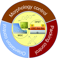
Organic semiconductors (OSCs) are promising materials for low-cost and large-area electronic devices because they can be processed from solution employing scalable and high-throughput meniscus-guided coating (MGC) techniques. Control over morphology and crystallinity of OSC thin films during MGC are one of the major challenges for achieving high-performance organic electronics toward real-world applications. In this review, we introduce and describe a series of representative MGC techniques that are used in the deposition of small-molecule OSC thin films, and the advantages and limitations of the different MGC methods are discussed. Further, we highlight recently reported strategies applied to control the morphology, molecular packing, and orientation of OSC thin films in the context of MGC techniques, and their impacts on the electronic properties of the resulting organic field-effect transistors (OFETs) are discussed. In addition, the underlying mechanisms of these strategies have been outlined, which gives us insight into how to tune the relevant parameters of MGC techniques to achieve the desired performance of OFETs. Finally, this review provides a comprehensive overview of the current challenges and opportunities in the field of OFETs, aiming to promote the future development of the small-molecule OSCs for large-area thin-film electronics.


image file: d0tc01887b-p1.tif

Wei Deng

Wei Deng received his B S degree from applied chemistry department at Nanjing Tech University in 2012. He obtained his PhD degree at Soochow University in 2017. After that, he joined institute of Functional Nano & Soft Materials, Soochow University as a lecturer. His research interests are focused on fabrication of organic thin films and their application in organic field-effect transistors and photodetectors. He has published over 30 journal papers, including Advanced Materials, Advanced Functional Materials, Nano Letters, ACS Nano, etc.

image file: d0tc01887b-p2.tif

Xiujuan Zhang

Xiujuan Zhang received her Ph D degree in chemistry from Technical Institute of Physics and Chemistry, Chinese Academy of Sciences (CAS) in 2006. After that, she worked as a postdoctoral fellow at City University of Hong Kong. In 2009, she joined institute of Functional Nano & Soft Materials (FUNSOM), Soochow University. Her research involves design and synthesis of small-molecule organic micro/nanocrystals and their application in opto/electronic devices. She has published over 110 articles in prestigious journals (including Nature Communications, Journal of the American Chemical Society, Angewandte Chemie, Advanced Materials, Nano Letters, etc.). Her publications have been cited over 3000 times and her H-index is 30.


1. Introduction

Organic field-effect transistors (OFETs) have attracted tremendous attention, because they are the central building blocks of organic electronics.1–9 Efforts over the past decade to engineer the molecular structure of conjugated small molecules and polymers have resulted in several families of organic semiconductors (OSCs) that exceed the mobility of the amorphous silicon (0.1–1 cm2 V−1 s−1)10,11 and even approach the mobility of polycrystalline silicon (>10 cm2 V−1 s−1).5,6,12,13 Compared with the conjugated polymers, small-molecule OSCs have always led the field in terms of high-performance devices.7 Besides the semiconductor molecular structures, the performance of OFETs also strongly depends on the grain size, degree of crystallinity, and grain orientation of the OSC thin films.12,14–18 Therefore, deposition approaches of OSC thin films would critically influence the device performance, often by orders of magnitude. For instance, relatively large grains in the blade-coated OSC thin films substantially reduce the density of grain boundaries and stacking faults in the OFET channel, compared with those in the vacuum-deposited microcrystalline OSC thin films.18 Thus, the OFET mobility remarkably improves, approximately a factor of ten. Highly oriented OSC thin films using solution-shearing method were found to show close to one order of magnitude a higher hole mobility compared with the spin-coated films with many spherulitic microstructures.19 In addition, real-world applications require the deposition approaches that can be easily scaled to large sizes and compatible with low-cost and continuous manufacturing.14,20

Meniscus-guided coating (MGC) techniques are widely recognized as an attractive route to achieve cost-effective, high-throughput and large-area organic electronics.14–16 Common MGC methods include dip coating, blade coating, slot-die coating, bar coating, solution shearing, hollow pen writing, zone casting, etc. In these techniques, when solution is injected into the gap between the coating head and the substrate, a meniscus (i.e., liquid–air interface) is formed and it connects the coating head to the substrate due to capillary action.21,22 Then, the meniscus is transmitted across the substrate by using the linear translation of either the substrate or the coating tool.14 Owing to the inherent directionality of the MGC process, these techniques can induce long-range ordered arrangement of organic molecules, forming oriented OSC crystalline films with large grain size.20 Moreover, unlike commonly used spin coating, these MGC techniques are quite amenable to be compatible with continuous and high-through roll-to-roll processing. Due to the complex crystallization kinetics of small-molecule OSCs in the solution phase, the morphology of OSC thin film is highly sensitive to the processing-related parameters, solvent properties, and substrate structure/type.14,16,20 Therefore, precise control of OSC thin-film morphology (grain size/shape, surface coverage, thickness, etc.), molecular packing, and crystallographic orientation are key challenges during the MGC process. In the past few years, a considerable amount of work has been conducted on the control of the morphology and orientation of small molecules and conjugated polymer thin films. These studies related to the conjugated polymers have been reviewed in many articles.14,23,24 However, the work about the organic small molecules in the related topic has not yet been systematically summarized and further discussion is needed.

In this review, we introduce and describe the major MGC techniques that are used in the deposition of small-molecule OSC thin films, and the advantages and limitations of the different MGC methods are discussed. Further, we highlight recently reported strategies used to control the morphology, molecular packing, and orientation of the OSC thin films during MGC processes. It can provide a mechanistic understanding of how coating-related parameters, solution properties, and substrate types to produce desired morphology and structure of the OSC thin films. Additionally, the effect of the morphology and structure on the electronic properties of the resulting OFETs is specifically discussed. This review aims to highlight some of the more recent, compelling areas of the fabrication of the small-molecule OSC thin films, while providing additional insight on the challenges of this field so as to guide future research efforts.

2. Meniscus-guided coating techniques

In general terms, MGC techniques all depend on a unidirectional and stable displacement of solution meniscus across the substrate surface. Therefore, these techniques can induce oriented and consecutive molecule assembly, achieving the control over morphology and crystallinity of the OSC thin films. In this section, we will introduce and describe a series of representative MGC techniques that are used in the deposition of small-molecule OSC thin films, as shown in Fig. 1. The advantages and limitations of different MGC methods are discussed as well.
image file: d0tc01887b-f1.tif
Fig. 1 Schematic summary of typical MGC techniques that are discussed in this article.

2.1 Dip coating

Dip coating is one of the most effective processes of thin film deposition, which has extensive applications in small-scale fabrication for academic researches and large-area commercial production.25,26 As its name implies, dip coating refers to the deposition of thin films via precision immersion and withdrawal of a substrate into a tank containing the object coating materials. There are several stages that occur during the dip-coating process: (i) immersion; (ii) dwelling; (iii) withdrawal; (iv) evaporation.27 In the immersion stage, the substrate is immersed into the solution of the coating OSCs at a slow speed (Fig. 2a). After the desired coating region is fully immersed, the substrate remains stationary, and then a small amount of solution climbs up the substrate, forming a meniscus (Fig. 2b). The meniscus is generated from a balance between gravity and the surface tension-based “capillary” forces. When the substrate is pulled out from the solution, the meniscus will be stretched owning to the pinning effect of the wettable substrate surface (Fig. 2c). Since the solvent evaporation rate near the meniscus front (i.e., contact line) is larger than that in the bulk solution, an outward convection flow (indicated by red arrows in Fig. 2d) is triggered to replenish the evaporation solvent loss and maintains the profile of the meniscus. The velocity (v) of the outward convective flow can be given by the Navier–Stokes eqn (1):28,29
 
image file: d0tc01887b-t1.tif(1)
where ρ is the density of solvent, t is time, Je refers to the evaporative flux of solvent, r is the height of the meniscus edge away from the bulk solution, and h is the horizontal distance of the meniscus at r, as shown in Fig. 2d. Considering the profile of the meniscus remains relatively stable during the whole dip-coating process, the ∂h/∂t term can be neglected. Thus, the eqn (1) can be rewritten as the eqn (2):
 
image file: d0tc01887b-t2.tif(2)

image file: d0tc01887b-f2.tif
Fig. 2 (a)–(d) Schematic diagram of the dip-coating process. Schematic illustration of the crystal (e) nucleation and (f) growth during dip coating. (g) Schematic illustration of the roll-to-roll dip-coating process.

According to the non-equilibrium one-sided model, (i) the Je obeys the Hertz–Knudsen law, (ii) the temperature and the pressure satisfy the Clausius–Clapeyron relation, and (iii) the reaction-limited evaporation occurs at the non-equilibrium interface. Thus, the v can be deduced by eqn (3):

 
image file: d0tc01887b-t3.tif(3)
K refers to the non-equilibrium parameter, and W is the thermal effect. According to the eqn (3), it can be derived that v of the outward convective flow increases sharply at the meniscus front. This will cause OSC molecules to flow from the bulk solution to the meniscus front and increases the local concentration of solute molecules near the meniscus front. When the solute concentration reaches saturation, the OSC molecules start to precipitate out to form nuclei near the contact line. With the outward flow persistently transporting the OSC molecules to the meniscus front, the supplied OSC molecules will aggregate onto the nucleation center and form seed crystals (Fig. 2e). In the subsequent dip-coating process, with the meniscus gradually pulling out, the continuous epitaxial growth of the seed crystals will occur, leading to the formation of continuous and oriented OSC thin films (Fig. 2f). According to the above statements, key parameters such as withdrawal velocity, substrate surface, solution property, play a key role in the morphology and structure of the obtained OSC thin films.

Dip coating is a relatively common technique in the literature because it is a lab-scale analog to industrial-scale coating methods.30Fig. 2g shows the schematic diagram of the roll-to-roll dip-coating process. The flexible substrate (e.g., polyimide film) is dipped into a bath of the solution, which generally has low viscosity. Then the flexible substrate is pulled out through a rotating roll. One of the main disadvantages of the process is that it needs a large solution storage tank to be able to fit commercial production. Therefore, low boiling point, volatile solvents are not applicable to the roll-to-roll dip-coating process.

2.2 Slot die coating

Slot die coating was originally developed in the early 1950s.31 In 1951 Eastman Kodak Co. filed the first patent principles for the slot die coating. After that, it was widely used in the paint industry. Recently, this coating technique has been applied for fabricating organic photovoltaic (OPV) cells, polymer light-emitting diodes (PLEDs), and OFETs, because of its simplicity, availability, and minimizing material waste.32–34 Slot die coating involves a hollow coating head where organic solution is pumped onto a moving substrate surface at a fixed height between the substrate and the coating head. Capillary forces hold the meniscus between the substrate and the coating head when the substrate is transmitted at a constant speed. The profile of meniscus strongly depended on the slot-die head. When a solution is injected into the slot-die head, it enters the gap between the head and the substrate and flows along the upstream and downstream directions in the two constrained channels. As the substrate moves, it results in shear flow in the channels. The flow rate varies linearly up the profile of the flow channel, and the flow rate of the solution is zero relative to the solid surface at the interface. Therefore, an extended meniscus is formed within the channel, as shown in Fig. 3a.
image file: d0tc01887b-f3.tif
Fig. 3 (a) Schematic representation of the typical formation process of meniscus in slot-die coating. (b) Schematic of a roll-to-roll slot-die system.

Fig. 3b shows a simplified schematic of a roll-to-roll slot-die system. The design of the roll-to-roll slot-die system plays around offering a uniform supplement of solution to the substrate surface. That is a very difficult requirement to do when transforming from a small coating area (about a few mm2) to large area. In order to address this demand, the slot-die coater is decomposed into multiple subsystems. It contains four subsystems: (i) metering management system: controls the flow velocity of the solution into the slot-die coater; (ii) distribution system: guarantees that the solution can be uniformly spread across the coating width; (iii) head positioning system: keeps the height of the coating head relative to the substrate; (vi) substrate motor system: decides how the substrate is passed through the coating head. Obviously, the roll-to-roll slot-die system is more complex than other roll-to-roll deposition systems, and the morphologies of the produced OSC thin films could be highly sensitive to the processing-related factors.

2.3 Blade coating and related techniques

Blade coating has recently emerged as a scalable fabrication method for OSC thin films.35–37 A lyophobic self-assembled monolayer (SAM)-functionalized Si wafer is chosen for the blade. This can prevent the OSCs from adhering to the blade. And the growth substrate is treated with a lyophilic layer, such as phenyltrichlorosilane (PTS), to guarantee a good wettability for organic solvent. The blade is placed at a fixed distance from the substrate surface (typically 100–500 μm). During the blade coating, a small amount of OSC solution is injected into the gap between the blade and the substrate surface, and then substrate or the blade moves at a constant velocity controlled by a motorized translation stage. OSC molecules will be deposited at the solid–liquid–air contact line, forming a thin film. This technique can also be adapted for continuous fabrication with roll-to-roll setups, in which the blade is stationary and the flexible substrate on a roller is in motion, as shown in Fig. 4. Solution shearing as a derived technique from blade coating recently has shown great potential in deposition of the high-crystallinity OSC thin films. In this method, a blade with a typical tilt angle of 5–10° is used. The angled blade can control the fluid flow within the solution and also effectively restrict the evaporation of the solution behind the blade. Therefore, using solution shearing, the crystallization process of OSCs can be controlled precisely, and OSC thin films with controlled crystallinity can be fabricated. When a cylindrical or rectangular bar is employed as a blade, this method is often referred to as “bar coating”, in which the bar hugs to the substrate surface during coating. Therefore, compared with the blade coating method, the meniscus is usually confined in a small space and this can induce geometrical confinement to prevent misaligned molecular packing. Although the bar coating has this advantage, using it to deposit small-molecule OSC thin films is rarely reported.
image file: d0tc01887b-f4.tif
Fig. 4 Schematic of a roll-to-roll blade-coating system.

2.4 Zone casting

Zone-casting technique derives from the zone refining process,38 which was first used in the early 1950s to purify germanium for transistors. In the zone-casting technique, the solution of OSCs is continuously supplied onto a moving substrate through a flat nozzle,39,40 and a meniscus will form between the flat nozzle and the substrate. As the solvent evaporation flux closer to the meniscus front is greater than the remaining parts, and thus the nucleation of solute molecules would take place within the narrow zone localized in the meniscus front. One of the main advantages of the zone casting is that it can provide a stable solution flow rate, which can determine the resulting thin film thickness. But when the zone casting is applied to the roll-to-roll processes, the nozzle can be readily blocked.

3. Morphology control strategies during meniscus-guided coating

Morphology of the OSC thin film, including grain size, surface coverage, and thickness, is closely related to the OFET performance. OSC thin films with larger grain size, higher surface coverage, and more thin thickness are desirable for use in high-performance OFET devices. In the last few years, new avenues have been explored for the control of OSC thin-film morphology during the MGC process. These recently developed morphology control strategies include controlling the coating speeds, solvent engineering, and blending with polymer binders. The underlying mechanism of these new strategies will be emphasized in this section to serve as an important foundation and guideline for future research.

3.1 Control of coating speed

MGC techniques rely on an external shearing force, for example, gravity in the dip coating or mechanical motion in the slot die coating, blade coating, and zone casting, to guide and control the molecular alignment in the OSC thin films. The intensity of these forces is determined by the coating speed; thus the coating speed has a strong influence on the morphology of the deposited OSC thin films. Many works have revealed the effect of the coating speed on the OSC thin-film texture.20,41–44 According to the morphologies of the OSC thin films obtained at different coating speeds, three regions can be distinguished. The first region is known as the evaporation regime, which is at low coating speeds. In this regime, the solvent evaporation is dominant over the viscous forces imposed by the substrate, resulting in a meniscus with nearly constant curvature up to the triple-phase contact line (Fig. 5a), indicating no viscous drag out at low coating speeds. In this case, the strong capillary force produced from the solvent evaporation would bring about the aggregation of the organic molecules on the meniscus front. As a result, thick and small crystal domains were observed (Fig. 5b), and even a stick-slip phenomenon would appear. As the coating speed increases, an obvious morphology transition will happen. Therefore, the relatively high coating speed region is referred to as the transition regime. In the transition regime, the viscous forces gradually paly role, and thus a partial meniscus is dragged out, leading to the formation of a liquid film in the meniscus front, as shown in Fig. 5c. The coating speeds in this regime are usually close to the rate of the solvent evaporation such that the contact line propagates along with the guided meniscus. In consequence, continuous and steady growth of organic crystals along the meniscus receding will occur, leading to the formation of oriented and millimeter-length OSC crystal domains (Fig. 5d). With further increase in the coating speeds, the Landau–Levich (LL) regime occurs in which viscous forces begin to dominate, while the solvent evaporation becomes negligible. As a result, a wet film is dragged out before the solvent evaporation, which can cause the pooling of solution on the substrate (Fig. 5e). With the solvent evaporation, an unguided crystallization process would occur in the pooling of the solution, resulting in anisotropic and spherulitic OSC film (Fig. 5f).42 The similar morphology evolution was also observed in the blade-coated polymer thin films.44
image file: d0tc01887b-f5.tif
Fig. 5 (a), (c) and (e) Schematic illustration of the meniscus shape comparing the three regimes. (b), (d) and (f) POM images of the OSC thin films produced from the three regimes. Reprinted with permission from ref. 42 Copyright 2011 Nature Publishing Group. (g) Schematic illustration of the edge-casting setup. (h) ve of nine pure solvents measured at different substrate temperatures. (i) Replotted the date in (h). (j)–(m) Typical POM images of the C8-BTBT thin films prepared at different coating speeds. Reprinted with permission from ref. 43 Copyright 2016 Wiley-VCH Verlag GmbH & Co. KGaA, Weinheim.

Apparently, the best morphology of OSC thin films appears in the transition regime where the receding speed of the solvent evaporation Ve is close to coating speed Vc. In order to predict the optimal coating speeds, Janneck et al. proposed an edge-casting method to measure Ve of a drying drop of pure solvent driven by evaporation only,43 schematically shown in Fig. 5g. In this technique, a meniscus was sustained at the edge of a structure and would recede as the solvent evaporated. During the solvent evaporation, the meniscus receding time over a given distance was recorded to obtain Ve by using a video camera. Fig. 5h shows the Ve of nine pure solvents during an edge-casting experiment measured at different substrate temperatures T. When the data points of Fig. 5h were replotted in a plot of ln(Ve/VMT0.7b) versus Tb/T, all of the experimental datas for different solvents fall together along one single line, as shown in Fig. 5i. This result indicates that the measured Ve at broad substrate temperatures could be well-fitted by the following eqn (4):

 
image file: d0tc01887b-t4.tif(4)
where A is the single fitting parameter, VM is the molar volume of the liquid solvent, ΔSvap is the entropy of vaporization of the solvent, R is the ideal gas constant, and Tb is the boiling point of the solvent at atmospheric pressure. Therefore, the values of Ve of different solvents at different temperatures can be predicted by eqn (4). To reveal the relationship between the value of the predicated Ve and Vc, the authors compared the morphologies of the OSC thin films fabricated at different normalized coating speed Vn = Vn/Vefe, 0.5, 1, 3, and 5. Organic semiconductors 2,7-dioctyl[1]benzothieno[3,2-b][1]benzothiophene (C8-BTBT) was chosen in this study because of its high solubility and high mobility. At Vn = 0.5 corresponding to the evaporation regime, the obtained C8-BTBT films were thick, and rough and small crystal aggregates were scattered on its surface (Fig. 5j). When coating at large speeds Vn > 1 (related to LL model), the crystal domains within the C8-BTBT films tended to narrow and thin. Eventually, the discontinuous and small crystal domains were observed at larger speed Vn = 5 (Fig. 5l). The C8-BTBT thin films produced at Vc = Ve (i.e., Vn = 1) had a smooth surface and well-interconnected crystal domains, presenting the best morphology (Fig. 5k). Meanwhile, OFETs based on the C8-BTBT thin films obtained at Vn = 1 showed more superior electrical characteristic with high mobility of 7 cm2 V−1 s−1, while maintaining low threshold voltage. Based on the experiment results, the optimal Vc had a good match with the calculated Ve, confirming the rationality of the prediction method.

3.2 Solvent engineering/optimization

Solvent type is one of the important factors in the final morphology and crystallization of OSC thin films.15 High boiling point solvent corresponds to a lower crystallization rate, which allows the molecules enough time to self-organize, and resulting in larger crystal domains. In fact, when high boiling point solvents were used in MGC techniques, the substrate needs to be heated up to raise the deposition efficiency of OSC thin films. However, the elevated substrate temperature would produce a temperature gradient along the air–liquid interface of the meniscus (Fig. 6a). The temperature gradient could induce the Marangoni flow from the bottom of the meniscus (high-temperature zone) to the top (low-temperature zone), as shown in Fig. 6b. This Marangoni flow would pull the molecules away from the front of meniscus and inhibit the formation of continuous and ideal OSC thin films. In order to reduce the negative effects, a mixed solvent system of dichlorobenzene (DCB)/m-xylene was used to create a countercurrent flow to compensate the loss of the molecules caused by the temperature-induced Marangoni flow.45 The DCB has a higher surface tension and lower volatility compared with the main m-xylene solvent. Due to the existence of temperature gradient, m-xylene around the tip of the front meniscus would evaporate first. With the evaporation loss of the m-xylene, a higher concentration zone of DCB would be formed, producing a surface tension gradient along the liquid–air interface of the meniscus. The surface tension gradient would induce another Marangoni flow from the lower to the higher surface tension regions, as indicated by the red arrows in Fig. 6c. Compared with the temperature-induced Marangoni flow, the surface tension-induced Marangoni flow would assist the mass transport of the OSC molecules toward the contact line, leading to an enhancement of molecule transport. So the concentration of OSC molecules at the contact line would reach supersaturation more quickly. In this scenario, the crystallization rate was improved, which can effectively promote two-dimensional (2D) growth of the OSC thin films. Meanwhile, the coating speed should be increased to match the improvement of the crystallization rate. As a result, thinner C8-BTBT thin films with fewer defects can be achieved at a higher coating speed of 1000 μm s−1. Accordingly, the mobility of the C8-BTBT thin films fabricated using the mixed solvent system shows an obvious improvement up to 16 cm2 V−1 s−1 with very good uniformity.
image file: d0tc01887b-f6.tif
Fig. 6 (a) Temperature distribution in the meniscus. (b) Simulation results of velocity distribution of the temperature-gradient-induced Marangoni flow. (c) Schematic illustration for the surface tension-induced Marangoni flow by blending m-xylene with DCB. Reprinted with permission from ref. 45 Copyright 2017 Wiley-VCH Verlag GmbH & Co. KGaA, Weinheim. (d) Mechanism schematic of “coffee ring” effect and Marangoni flow. POM image of C8-BTBT thin films produced from (e) a mixture of toluene and carbon tetrachloride and (f) a single solvent carbon tetrachloride. Reprinted with permission from ref. 46 Copyright 2019 Wiley-VCH Verlag GmbH & Co. KGaA, Weinheim.

A non-uniform film is commonly observed in most MGC processes, resulting from the well-known “coffee ring” effect. The key to this effect is that the contact line of the liquid film is pinned during drying and an evaporation-induced convective flow of the solvent transports the solutes from the bulk meniscus to the contact line. A very powerful strategy to reduce the “coffee ring” effect is the introduction of another flow that can counterbalance the convective flow. Dong et al. intentionally created a Marangoni flow in the fluid by using a mixture of toluene and carbon tetrachloride as organic semiconductor C8-BTBT solvent.46 Carbon tetrachloride is a low boiling point solvent with high surface tension while toluene has a high boiling point and low surface tension. Because the evaporation rate at the contact line was much faster than that at the interior region of the meniscus, a higher concentration region of toluene would form near the contact line. Thus, the surface tension near the contact line was relatively lower than that in the meniscus inferior because of the low surface tension of toluene, producing a surface tension gradient in the meniscus. This surface tension gradient would induce a Marangoni flow from the contact line to the bulk meniscus and produce a recirculation flow in the meniscus, as shown in Fig. 6d. The recirculation flow favors the production of a uniform C8-BTBT thin film on the substrate and the coverage of the ribbon-like C8-BTBT crystals was over 60% (Fig. 6e). However, when a single solvent was used, it was obvious that the OSC molecules were unevenly distributed on the substrate, and the coverage of OSC thin film was less than 25% (Fig. 6f), which is adverse to the practical device application.

3.3 Blending with polymer binder

Due to the low viscosity and dewetting propensity of the small-molecule OSC solution, fabrication of OSC crystalline thin films with high coverage and uniformity remains a significant challenge.12,47–50 Therefore, the reproducibility and homogeneity of device performance over large substrate areas have been limited. Blending small-molecule OSCs with insulating polymers has recently been demonstrated as an effective way for improving the OFET reproducibility and uniformity. The polymer, such as polystyrene (PS), polymethylmethacrylate (PMMA), or poly(alpha-methyl styrene) (PαMS), acts as a binder and can help to overcome the common issues about solution dewetting and optimize the morphology and crystallinity of the OSC thin films, achieving a good uniformity of device performance over large areas. Pisula et al. investigated the α,ωdihexylquaterthiophene (DH4T) thin film formation during dip coating by blending with PMMA binder.51 In order to understand the role of the polymer binder, the authors carried out a systematic study on the effects of the weight fraction (wt%) and molecular weight (Mw) of the PMMA on the OSC thin film morphology, crystallinity, and charge carrier transport. With increasing the wt% of PMMA from 2 to 5 and 10 wt%, the coverage of the obtained dendritic crystals would gradually improve (Fig. 7a). And the mobilities of the DH4T thin films with 10 wt% PMMA increased by two and six times compared with the DH4T thin films fabricated from 5 and 2 wt% PMMA, respectively. The authors also observed that the coverage density of crystalline ribbons significantly enhanced when increasing the Mw of PMMA (Fig. 7b), and thereby the highMw PMMA results in higher carrier mobilities. The morphology and mobility improvement of the OSC thin films prove that the blending of a certain fraction of polymer binder can enhance the crystallization of small-molecule OSCs. Further, the authors performed COMSOL simulation to account for the origin of the improved crystallization. The simulated result, as shown in Fig. 7c, exhibited an obvious viscosity gradient at the meniscus, and an even higher viscosity appeared near the meniscus front (i.e., contact line) due to the increased solution concentration caused by solvent evaporation. The viscosity gradient would facilitate the draw of solutes and increase molecule transport from solution to the contact line. Since the supersaturation of PMMA is lower than that of the OSC molecules, the PMMA molecules are more prone to solidify on the substrate surface than the OSC molecules (Fig. 7d). The solidified bottom PMMA layer would reduce the nucleation barrier and points of the small molecule OSCs, which can suppress the random creation of spontaneous nucleation. Similarly, Niazi et al. also observed that the morphology and device performance of the 2,8-difluoro-5,11-bis(triethylsilylethynyl) anthradithiophene (Dif-TES-ADT) thin films could be improved by blending with polymer binder using blade coating.52 In this work, the authors found that the topography of Dif-TES-ADT: PS blends be more continuous and less defective as compared with the PaMS-based blends (Fig. 7e). This is because PS has lower glass transition temperature of ∼100 °C than that of PαMS (∼170 °C), which is likely to form a higher viscosity of PS blend solution to help to yield more continuous films. Moreover, the Dif-TES-ADT thin films in condition of high coating speed show spherulite-like crystals with large size and no topographic defects, such as gaps and cracks, existed within the spherulites, which is the main morphological reason for the better device performance observed at high blade-coating speed. Beyond the morphological reason, another important contributing factor is the vertical phase separation, and the bottom PS layer (Fig. 7f) has been proved to have the ability to reduce the interfacial trap state density.
image file: d0tc01887b-f7.tif
Fig. 7 POM images of the DH4T:PMMA films obtained from different (a) weight fractions of PMMA and (b) MWs of PMMA. (c) COMSOL simulation of the dynamic viscosity at the meniscus of the DH4T:PMMA/CHCl3 solution. (d) Schematic illustration for the dip-coating of DH4T:PMMA. Reprinted with permission from ref. 51 Copyright 2018 Wiley-VCH Verlag GmbH & Co. KGaA, Weinheim. (e) POM images of the Dif-TES-ADT:PaMS and Dif-TES-ADT:PS thin films. (f) Cross-sectional TEM image of the bilayer stratification of the blend with PS at the bottom and Dif-TES-ADT on top. Reprinted with permission from ref. 52 Copyright 2015 Nature Publishing Group.

4. Molecular packing control of the OSC thin films

Besides thin film morphology, the performance of the OFETs is also closely related to the molecular packing motif in the deposited OSC thin films. In organic semiconductors, the molecular packing motifs determine the π–π stacking distance between cofacially stacked molecules, and hence it can critically affect the charge carrier mobility.42 Since organic molecules are loosely bonded by van der Waals forces in the solid state, external forces will be easy to induce molecular packing reorganization, forming non-equilibrium states or even polymorphism.53 Recently, electric field-induced and solution-shearing methods have proven to allow access to the metastable non-equilibrium molecular packing motifs.42,54 These strategies used in the MGC will be discussed in the following section.

4.1 Electric field

Neutral particles will occur electrokinetic motion, when the particle is placed in an asymmetric electric field.55 This phenomenon is first defined as dielectrophoresis (DEP) by Pohl. Thus, electric field has great potential as an external stimulus to change the packing motifs of neutral small-molecule OSCs to obtain different polymorphs. Toney et al. first reported that the application of alternating AC electric fields could modify the molecular packing motifs in the solution-shearing coated small-molecule OSC thin films and tune their electrical performance.54Fig. 8a shows the schematic diagram of the utilized experimental equipment. In this system, the edge of the blade was used as a sharp-edge electrode to apply a voltage, and the sharp-edge electrode is very necessary because it can intensify the electric field, reaching locally values close to the breakdown of common solvents, i.e., ∼107 V m−1. Therefore, strong DEP forces and torques would be produced near the blade edge. Since the whole frequency spectrum for chlorobenzene (CB) solvent is negative value, which can produce a negative DEP force to push the molecules away from high electric field areas, CB was selected as the solvent. Fig. 8b shows a theoretical estimation of the drift velocity of C8-BTBT molecules dissolved in CB under an AC voltage of 150 V at 100 Hz, and a maximum velocity of ∼1 μm s−1 was achieved near the blade edge. In order to make sure that the C8-BTBT molecules have enough time to move in the solution and crystallize close to the blade, a low coating speed was need to match the low drift velocity of molecule. Therefore, a sharp blade with 5 μm of radius of curvature was adopted, and a low speed of 50 μm s−1 was used to shear the solution of C8-BTBT in CB solvent. The shear coating process could achieve C8-BTBT crystalline thin film with large single crystallites, and the electric field applied at the blade edge could produce a strong DEF force, which could allow to tune the molecular packing within the resulting C8-BTBT thin films. They observed a significant change in the unit-cell structure as the DEP force increased (Fig. 8c), and metastable polymorphs, some of them unprecedented, were obtained. As a consequence, a twofold enhancement in the OFET mobilities was found for C8-BTBT thin films along the transport direction.
image file: d0tc01887b-f8.tif
Fig. 8 (a) Schematic diagram of the utilized experimental equipment to apply DEP forces during solution-shearing coating of small-molecule OSC thin films. (b) Calculation result of the drift velocity of C8-BTBT molecules in CB solvent under an AC electric field. (c) Length evolution of the a and b-axes with the DEP force increased. Reprinted with permission from ref. 54 Copyright 2017 Wiley-VCH Verlag GmbH & Co. KGaA, Weinheim. (d) The evolution of the (101) and (010) Bragg peak of the TIPS-pentacene thin films obtained from different shearing speeds. (e) Molecular packing structure of the evaporated TIPS-pentacene thin film and the thin film prepared at a high shearing speed of 8 mm s−1. (f) Lattice strain and (g) charge transport properties as a function of the shearing speeds. Reprinted with permission from ref. 42 Copyright 2011 Nature Publishing Group.

4.2 Shear strain

Shear strain method was first applied to OSCs by Giri and coworkers for growing 6,13-bis(triisopropylsilylethynyl)pentacene (TIPS-pentacene) crystals.42 They reported that a high shearing speed could induce large shear strain within the OSC molecules, producing strained TIPS-pentacene thin films. The in-plane lattice parameters (a and b) of the TIPS-pentacene thin films incrementally change with the solution-shearing speed. To study the lattice strain evolution with the shearing speed, high-resolution grazing incidence X-ray diffraction (GIXRD) measurements were performed. With the shearing speed increases, the (101) d-spacing decreases generally, from 7.70 to 7.26 Å, and concurrently the (010) d-spacing increases incrementally, from 7.83 to 8.13 Å (Fig. 8d). Although the in-plane unit cell geometry of the obtained TIPS-pentacene crystals became increasingly more oblique with increasing shearing speed, while the in-plane unit cell area remained comparatively constant. Compared with the molecular packing structure of the evaporated TIPS-pentacene film (unstrained films), the crystal structure for the strained film prepared at a high shearing speed of 8 mm s−1 displayed a more oblique molecular packing motif and decreased π–π stacking distance of 3.08 Å, as shown in Fig. 8e. Accordingly, the charge carrier mobility increased from 0.8 cm2 V−1 s−1 for unstrained films deposited at 0.4 mm s−1 to a high mobility of 4.6 cm2 V−1 s−1 for the strained film (Fig. 8f and g). The strained crystal lattice is thermally stable up to 160 °C. However, when the strained films were exposed to toluene vapor for an hour, the position of the GIXRD peak had changed dramatically, and the lattice spacing of the strained films became similar to that of the evaporated TIPS-pentacene film (unstrained film), indicating that the strained crystal lattice is metastable and occurs strain relief. In some reports, shear strain method has also been shown to reduce the π–π stacking distance in the conjugated polymer films.7

5. Control strategies of crystallization orientation during meniscus-guided coating

While control of the morphology and molecular packing motifs are indeed crucial for tuning the final OFET performance, direct manipulation of the crystallization orientation of OSCs relative to the carrier transport direction, not only can impart favourable performance to each device, but also can reduce the device-to-device variations and ensure the uniformity of the fabricated device arrays.56–58 This is attributed to the fact that the optimal charge transport direction is along the strongest π orbitals overlap direction, however, charge transport in weak van der Waals bonded OSCs often exhibit anisotropic properties.9,13 Although the MGC techniques provide a unidirectional stress field to align OSC molecules, obtaining OSC thin films always exhibit non-uniform orientation due to stochastic nucleation and instabilities of fluid flow during the growth process. To overcome these problems, several groups have recently investigated strategies to control the crystalline orientation of the OSC molecules during MGC. We will review these approaches that have been employed for achieving the uniaxial alignment of small-molecule OSC thin films in the following section.

5.1 Solution epitaxial growth

Solution epitaxy is a promising approach for the controlled growth of oriented OSC thin films with highly aligned crystal domains through solution-phase processing methods. The pioneer work on solution epitaxial growth of OSC crystals was reported by Hu et al.59 In this work, the solution epitaxy process involves two steps, as illustrated in Fig. 9a–d. First, micrometer-sized organic crystals were fabricated by drop casting of microliters of OSC solution on the substrate (Fig. 9a and b). Second, the micrometer-sized organic crystals were used as seed crystals, and the same OSC solution was dropped on the small-sized crystals. When the new solution was added, a portion of the small crystal was dissolved (Fig. 9c), and then the epitaxial growth of the small organic crystals occurred in the solution. Finally, the micrometer-sized organic crystals epitaxially grown into millimeter or centimeter-sized organic crystals (Fig. 9d), and the orientation of the large crystal was determined by the seed crystal (that is the small crystal). More importantly, the solution epitaxial growth method is also applicable to many different small-molecule OSCs, showing a broad universality.
image file: d0tc01887b-f9.tif
Fig. 9 (a)–(d) Schematic showing that solution epitaxy process of OSC crystals. Reprinted with permission from ref. 59 Copyright 2016 Wiley-VCH Verlag GmbH & Co. KGaA, Weinheim. (e) Schematic diagram for the two-step bar coating method. (f) and (g) POM images of the single-crystalline OSC thin films obtained by two-step bar coating method. (h) Transfer curves of the all 225 OFETs. (i) Mobility distribution of the 225 devices. Reprinted with permission from ref. 57 Copyright 2018 American Chemical Society.

Recently, Chan et al. demonstrated the use of two-step bar coating to achieve the solution epitaxial growth of uniaxially oriented C8-BTBT thin films over large areas.57 The procedures are described in Fig. 9e. Polycrystalline C8-BTBT thin films with centimeters long and millimeter wide 1D crystals were formed on the whole substrate after the first bar coating. Then the substrate was rotated by 90°, and one of the long 1D crystal domains with a sharp boundary was chosen to serve as the crystal seeds to perform the second bar-coating process (Fig. 9f). After that, single-crystalline C8-BTBT thin films composed of consistently oriented 1D crystal domains were successfully fabricated. The formation mechanism of the single-crystalline OSC thin films was investigated. From the polarized optical microscope (POM) image (Fig. 9g), it can be concluded that while the crystallographic orientation between the 1D crystals developed by the first bar coating is inconsistent, each 1D crystal has the same orientation along the first coating direction. When the long axis of the 1D crystal was employed as crystal seeds, the epitaxial growth of the crystals would occur during the second bar-coating process, leading to the formation of the 1D crystal domains with pure orientation. Moreover, the second bar-coated 1D crystals followed the orientations of the crystal seed completely. By unifying the crystallographic orientation of the crystal domains in the C8-BTBT thin films, 225 OFETs showed similar transfer curves and uniform carrier mobility distribution (Fig. 9h and i). In addition, the average mobility of the 225 OFETs exhibited a 40% enhancement compared with the first bar-coated devices.

5.2 Control of nucleation

Crystallization of OSCs is composed of two steps: nucleation and crystal growth. Nucleation involves overcoming of a free energy barrier and is intrinsically stochastic. This property often leads to random distribution of nucleation size, site, and orientation during MGC. And the crystal domains within the OSC thin films fabricated from the MGC techniques exhibit in general non-uniform crystal morphologies, qualities, and crystallographic orientations, resulting in great variations in electronic properties. Therefore, it is particularly important to control nucleation for the fabrication of highly uniform and oriented OSC thin films. There have been relatively few methods reported on the control of OSC nucleation from solution, as summarized below.

In the MGC techniques, nucleation often preferentially occurs at the meniscus front. However, the areas of the meniscus fronts (width of several millimeters to several centimeters or larger) are much larger than the size of OSC nuclei (several tens to several hundreds of nanometers), uncontrollable and random nucleation would happen. Therefore, the key to controlling nucleation depends on the control over size of the meniscus front. Recently, Deng et al. reported an approach—channel-restricted meniscus self-assembly (CRMS)—that allows for the growth of highly oriented and uniform OSC single crystals.56 The CRMS strategy combines microscale photoresist (PR) channels with dip coating. The process is schematically shown in Fig. 10a. The typical PR channel width and depth are 5 μm and ∼800 nm, respectively. When the PR microchannel was immersed into the organic solution, the solution would move up due to the surface tension effect and capillary force. Then it would soon split due to the large surface energy difference between PR stripes and SiO2 channels, yielding a meniscus between two adjacent PR stripes. Computational fluid dynamics (CFD) simulation shows that the profile curve of the meniscus follows the parabolic equation, and the size of meniscus front diminishes to hundreds of nanometers (Fig. 10b). The nanoscale meniscus front ensures the exclusive nucleation and growth of organic crystals along the lateral sides of the PR stripes to avoid the heterogeneous nucleation that usually occurs in conventional MGC method. In the subsequent dip-coating process, the operating tensile force for substrate liftoff will pin the solution meniscus edge at the lateral surface of the PR stripes. With the outward flow persistently transporting solute to the edge of the meniscus, the continuous epitaxial growth of crystals along the PR sidewalls will occur, leading to the formation of oriented film separating by OSC single crystals with unitary growth direction (Fig. 10c). In contrast, when the substrate without the microchannels was used, the obtained OSC film was made of many dendritic crystal domains with an inconsistency of crystallographic orientation (Fig. 10d). Using CRMS, the authors fabricated 2,6-diphenylanthracene (DPA) thin films that were composed of aligned 1D single-crystal arrays, showing a record high average mobility up to 30.3 cm2 V−1 s−1 (at the time of the publication).


image file: d0tc01887b-f10.tif
Fig. 10 (a) Schematic illustration of the CRMS strategy for growth of highly oriented and uniform OSC single crystals. (b) CFD simulation result of the confined meniscus within the microscale PR channels. POM image of the DPA crystal arrays fabricated by (c) CRMS method and (d) conventional MGC method. Reprinted with permission from ref. 56 Copyright 2019 Elsevier Ltd. (e) Design of wetting/dewetting regions for nucleation control. (f) POM images of the single-crystal-like TIPS-pentacene thin film obtained using nucleation control method. Reprinted with permission from ref. 19 Copyright 2013 Nature Publishing Group.

Another approach to control nucleation is inspired by the mechanism behind the “coffee ring” effect. In the “coffee ring” effect, crystal nucleation preferentially occurs at highly convex points along the contact line.60 According to this one characteristic, Bao et al. purposefully manipulated the shape of the contact line by patterning the substrate with solvent-wetting and dewetting regions, using a combination of photolithography and surface modification.19 The initial parts of the wetting regions are shaped as triangles with their tips pointing towards the approaching solution meniscus, as shown in Fig. 10e. When the meniscus got through the wetting regions, the contact line was temporarily pinned at the triangle boundary, until nucleation took place at the tips. The design of triangular wetting regions can produce a wedge-shaped meniscus that could funnel the convective supply of solute towards the tip. This would shorten the nucleation induction time at the tip, achieving preferential nucleation at the small-sized tip position. In addition, the triangle tips are designed to reduce the density of nucleation events, facilitating the formation of single crystal nucleus. Combining the control of nucleation and solution shearing, the authors achieved large-area TIPS-pentacene thin films that having high probability of single-crystalline domains (>90% with 200 mm wide patterns, Fig. 10f). The single-crystal-like TIPS-pentacene thin films dramatically boosted the hole mobility to higher than 10 cm2 V−1 s−1, the highest reported value so far for this extensively studied material.

6. Conclusions and outlook

In the area of OFETs, it is imperative to find out techniques for low-cost, high-throughput, and large-area deposition of OSC thin films, ensuring real-world device applications. MGC techniques have been shown to be effective techniques to achieve this goal because it can be compatible with continuous roll-to-roll processing. In order to gain high-performance devices, the morphology and crystallinity of the OSC thin films fabricated from the MGC need to be strictly controlled. So far, different strategies have been reported to control the morphology, molecular packing, and the orientation of the OSC thin films, which are systematically discussed in this review. Benefiting from these strategies, to date, small-molecule thin film-based OFETs have made great progress, as shown in Table 1. And the state-of-the-art the OFETs have achieved high values, which are higher than the most reports for the polymer OFETs.23,61–69 More excitingly, by using the control strategies of crystallization orientation, single-crystalline OSC thin films were successfully fabricated, which enabled record-setting charge carrier mobility of 30.3 cm2 V−1 s−1.
Table 1 Mobilities of the small-molecule OSC thin films fabricated from different methods
Method Materials Structure Mobility (cm2 V−1 s−1) Ref.
Morphology control strategies Control of coating speed C8-BTBT Thin film 5.7 43
Solvent engineering/optimization C8-BTBT Thin film 23.5 46
Blending with polymer binder DiF-TES-ADT Thin film 6.7 52
Molecular packing control Electric field TIPS-pentacene Thin films 3.7 54
Shear strain TIPS-pentacene Thin film 4.6 42
Control strategies of crystallization orientation Solution epitaxial growth C8-BTBT Single-crystalline thin film 14.9 57
Control of nucleation DPA Aligned single-crystal array 39.3 56


Despite these advances, looking ahead, there are still many challenges that need to be addressed before coming to a new era of organic electronics. First, considering that cost is an important factor for industrial production, high throughput involving high deposition speed (e.g., >17 mm s−1) and low temperature (e.g., ambient conditions) both are desirable for industrial scale-up.14 However, the reported deposition speeds for the OSC thin films under ambient conditions are still very low (<1 mm s−1). From the perspective of OSC growth kinetics, rapid crystallization at low temperature generally results in OSC thin films with low crystallinity, high defect density, and small grains, which reduce the efficiency of charge transport in OSC thin films. Therefore, fast and room-temperature deposition of OSC thin films still remains a challenge. Second, compared to inorganic materials, OSCs are more suitable for flexible device applications, since they have the inherent advantage of superior mechanical properties.70,71 However, high-quality OSC thin films are difficult to be deposited on the flexible substrates. The main reason for this is that the deposition process of the OSC thin films for the flexible substrates may be limited by their rough and non-wettable surface, processing temperature, and incompatibility with solvents, meaning that the requirements of MGC methods for depositing the high-quality OSC thin films on flexible substrates are more stringent.72,73 Third, although the mobility of OSC thin films fabricated by the MGC is sufficient for many practical applications, these applications require the location of the OSC thin films in a specifically patterned structure.74,75 Patterning of OSC thin films not only can guarantee device uniformity and reproducibility, but also can reduce the cross-talk between neighbouring devices. However, current patterning methods for OSCs are incompatible with the low-cost, high-throughput MGC techniques. Consequently, greater effort should be expended to develop new patterning strategies for ensuring the construction of high-performance, low-cost, and large-area organic integrated devices. In spite of these challenges, worldwide research efforts on the solution deposition technique continue to be developed, and it will give us confidence that most of these challenges will be successfully met in the near future.

Conflicts of interest

There are no conflicts to declare.

Acknowledgements

This work was supported by the National Natural Science Foundation of China (Grant No. 61904117, 51821002, and 51672180), the Natural Science Foundation of Jiangsu Province of China (BK20180845), the Priority Academic Program Development of Jiangsu Higher Education Institutions (PAPD), the 111 Project, and Collaborative Innovation Center of Suzhou Nano Science and Technology (Nano-CIC).

References

  1. C. Jiang, H. W. Choi, X. Cheng, H. Ma, D. Hasko and A. Nathan, Science, 2019, 363, 719–723 CrossRef CAS PubMed.
  2. M. Nikolka, I. Nasrallah, B. Rose, M. K. Ravva, K. Broch, A. Sadhanala, D. Harkin, J. Charmet, M. Hurhangee, A. Brown, S. Illig, P. Too, J. Jongman, I. McCulloch, J.-L. Bredas and H. Sirringhaus, Nat. Mater., 2016, 16, 356–362 CrossRef PubMed.
  3. A. Gumyusenge, D. T. Tran, X. Luo, G. M. Pitch, Y. Zhao, K. A. Jenkins, T. J. Dunn, A. L. Ayzner, B. M. Savoie and J. Mei, Science, 2018, 362, 1131–1134 CrossRef CAS PubMed.
  4. W. Deng, X. Zhang, R. Jia, L. Huang, X. Zhang and J. Jie, NPG Asia Mater., 2019, 11, 77 CrossRef CAS.
  5. X. Xu, Y. Yao, B. Shan, X. Gu, D. Liu, J. Liu, J. Xu, N. Zhao, W. Hu and Q. Miao, Adv. Mater., 2016, 28, 5276–5283 CrossRef CAS PubMed.
  6. A. Yamamura, S. Watanabe, M. Uno, M. Mitani, C. Mitsui, J. Tsurumi, N. Isahaya, Y. Kanaoka, T. Okamoto and J. Takeya, Sci. Adv., 2018, 4, eaao5758 CrossRef PubMed.
  7. H. Sirringhaus, Adv. Mater., 2014, 26, 1319–1335 CrossRef CAS PubMed.
  8. W. Deng, B. Lu, J. Mao, Z. Lu, X. Zhang and J. Jie, ACS Appl. Mater. Interfaces, 2019, 11, 36205–36212 CrossRef CAS PubMed.
  9. C. Reese and Z. Bao, Mater. Today, 2007, 10, 20–27 CrossRef CAS.
  10. S. Duan, T. Wang, B. Geng, X. Gao, C. Li, J. Zhang, Y. Xi, X. Zhang, X. Ren and W. Hu, Adv. Mater., 2020, 32, 1908388 CrossRef CAS PubMed.
  11. W. Deng, X. Zhang, L. Wang, J. Wang, Q. Shang, X. Zhang, L. Huang and J. Jie, Adv. Mater., 2015, 27, 7305–7312 CrossRef CAS PubMed.
  12. Y. Yuan, G. Giri, A. L. Ayzner, A. P. Zoombelt, S. C. B. Mannsfeld, J. Chen, D. Nordlund, M. F. Toney, J. Huang and Z. Bao, Nat. Commun., 2014, 5, 3005 CrossRef PubMed.
  13. H. Minemawari, T. Yamada, H. Matsui, J. Tsutsumi, S. Haas, R. Chiba, R. Kumai and T. Hasegawa, Nature, 2011, 475, 364–367 CrossRef CAS PubMed.
  14. X. Gu, L. Shaw, K. Gu, M. F. Toney and Z. Bao, Nat. Commun., 2018, 9, 534 CrossRef PubMed.
  15. S. Riera-Galindo, A. Tamayo and M. Mas-Torrent, ACS Omega, 2018, 3, 2329–2339 CrossRef CAS PubMed.
  16. Y. Diao, L. Shaw, Z. Bao and S. C. B. Mannsfeld, Energy Environ. Sci., 2014, 7, 2145–2159 RSC.
  17. H. H. Choi, A. F. Paterson, M. A. Fusella, J. Panidi, O. Solomeshch, N. Tessler, M. Heeney, K. Cho, T. D. Anthopoulos, B. P. Rand and V. Podzorov, Adv. Funct. Mater., 2019, 29, 1903617 Search PubMed.
  18. Z. Zhou, Q. Wu, S. Wang, Y.-T. Huang, H. Guo, S.-P. Feng and P. K. L. Chan, Adv. Sci., 2019, 6, 1900775 CrossRef CAS PubMed.
  19. Y. Diao, B. C.-K. Tee, G. Giri, J. Xu, D. H. Kim, H. A. Becerril, R. M. Stoltenberg, T. H. Lee, G. Xue, S. C. B. Mannsfeld and Z. Bao, Nat. Mater., 2013, 12, 665–671 CrossRef CAS PubMed.
  20. M. Chen, B. Peng, S. Huang and P. K. L. Chan, Adv. Funct. Mater., 2019, 30, 1905963 CrossRef.
  21. W. Deng, X. Zhang, L. Huang, X. Xu, L. Wang, J. Wang, Q. Shang, S.-T. Lee and J. Jie, Adv. Mater., 2016, 28, 2201–2208 CrossRef CAS PubMed.
  22. M. He, B. Li, X. Cui, B. Jiang, Y. He, Y. Chen, D. O’Neil, P. Szymanski, M. A. EI-Sayed, J. Huang and Z. Lin, Nat. Commun., 2017, 8, 16045 CrossRef CAS PubMed.
  23. M. Pandey, N. Kumari, S. Nagamatsu and S. S. Pandey, J. Mater. Chem. C, 2019, 7, 13323 RSC.
  24. M. Richard, A. Al-Ajaji, S. Ren, A. Foti, J. Tran, M. Frigoli, B. Gusarov, Y. Bonnassieux, E. G. Caurel, P. Bulkin, R. Ossikovski and A. Yassar, Adv. Colloid Interface Sci., 2020, 275, 102080 CrossRef PubMed.
  25. S. Nam, J. Jang, J. E. Anthony, J.-J. Park, C. E. Park and K. Kim, ACS Appl. Mater. Interfaces, 2013, 5, 2146–2154 CrossRef CAS PubMed.
  26. L. Li, P. Gao, W. Wang, K. Mllen, H. Fuchs and L. Chi, Angew. Chem., Int. Ed., 2013, 52, 12530–12535 CrossRef CAS PubMed.
  27. K. Wu, H. Li, L. Li, S. Zhang, X. Chen, Z. Xu, X. Zhang, W. Hu, L. Chi, X. Gao and Y. Meng, Langmuir, 2016, 32, 6246–6254 CrossRef CAS PubMed.
  28. J. Xu, J. Xia, S. W. Hong, Z. Lin, F. Qiu and Y. Yang, Phys. Rev. Lett., 2006, 96, 066104 CrossRef PubMed.
  29. B. J. Fischer, Langmuir, 2002, 18, 60–67 CrossRef CAS.
  30. J. Park, K. Shin and C. Lee, Int. J. Precis. Eng. Manuf., 2016, 17, 537–550 CrossRef.
  31. C.-F. Lin, B.-K. Wang, C. Tiu and T.-J. Liu,, Adv. Polym. Technol., 2013, 32, 249–257 CrossRef.
  32. Y. Galagan, H. Fledderus, H. Gorter, H. H. ’t Mannetje, S. Shanmugam, R. Mandamparambil, J. Bosman, J.-E. J. M. Rubingh, J.-P. Teunissen, A. Salem, I. G. de Vries, R. Andriessen and W. A. Groen, Energy Technol., 2015, 3, 834–842 CrossRef CAS.
  33. B. Park, O. E. Kwon, S. H. Yun, H. G. Jeon and Y. H. Huh, J. Mater. Chem. C, 2014, 2, 8614–8621 RSC.
  34. B. Park, I.-G. Bae, O. E. Kwon and H. G. Jeon, RSC Adv., 2016, 6, 101613 RSC.
  35. J. Y. Seok and M. Yang, Adv. Mater. Technol., 2016, 1, 1600029 CrossRef.
  36. B. Dorling, V. Vohra, T. T. Dao, M. Garriga, H. Murata and M. Campoy-Quiles, J. Mater. Chem. C, 2014, 2, 3303–3310 RSC.
  37. K. W. Chou, H. U. Khan, M. R. Niazi, B. Yan, R. Li, M. M. Payne, J. E. Anthony, D.-M. Smilgies and A. Amassian, J. Mater. Chem. C, 2014, 2, 5681–5689 RSC.
  38. N. R. Munirathnam, D. S. Prasad, C. Sudheer, A. J. Singh and T. L. Prakash, Bull. Mater. Sci., 2002, 25, 79–83 CrossRef CAS.
  39. Y. Su, X. Gao, J. Liu, R. Xingab and Y. Han, Phys. Chem. Chem. Phys., 2013, 15, 14396–14404 RSC.
  40. F. Paulus, J. U. Engelhart, P. E. Hopkinson, C. Schimpf, A. Leineweber, H. Sirringhaus, Y. Vaynzof and U. H. F. Bunz, J. Mater. Chem. C, 2016, 4, 1194–1200 RSC.
  41. S. Galindo, A. Tamayo, F. Leonardi and M. Mas-Torrent, Adv. Funct. Mater., 2017, 27, 1700526 CrossRef.
  42. G. Giri, E. Verploegen, S. C. B. Mannsfeld, S. Atahan-Evrenk, D. H. Kim, S. Y. Lee, H. A. Becerril, A. Aspuru-Guzik, M. F. Toney and Z. Bao, Nature, 2011, 480, 504–508 CrossRef CAS PubMed.
  43. R. Janneck, F. Vercesi, P. Heremans, J. Genoe and C. Rolin, Adv. Mater., 2016, 28, 8007–8013 CrossRef CAS PubMed.
  44. K. S. Park, J. J. Kwok, R. Dilmurat, G. Qu, P. Kafle, X. Luo, S.-H. Jung, Y. Olivier, J.-K. Lee, J. Mei, D. Beljonne and Y. Diao, Sci. Adv., 2019, 5, eaaw7757 CrossRef PubMed.
  45. Z. Zhang, B. Peng, X. Ji, K. Pei and P. K. L. Chan, Adv. Funct. Mater., 2017, 27, 1703443 CrossRef.
  46. Z. Wang, H. Guo, J. Li, L. Wang and G. Dong, Adv. Mater. Interfaces, 2019, 6, 1801736 CrossRef.
  47. K. Haase, C. T. d. Rocha, C. Hauenstein, Y. Zheng, M. Hambsch and S. C. B. Mannsfeld, Adv. Electron. Mater., 2018, 4, 1800076 CrossRef.
  48. K. Zhao, O. Wodo, D. Ren, H. U. Khan, M. R. Niazi, H. Hu, M. Abdelsamie, R. Li, Er. Q. Li, L. Yu, B. Yan, M. M. Payne, J. Smith, J. E. Anthony, T. D. Anthopoulos, S. T. Thoroddsen, B. Ganapathysubramanian and A. Amassian, Adv. Funct. Mater., 2016, 26, 1737–1746 CrossRef CAS.
  49. M. Kang, H. Hwang, W.-T. Park, D. Khim, J.-S. Yeo, Y. Kim, Y. Kim, Y.-Y. Noh and D.-Y. Kim, ACS Appl. Mater. Interfaces, 2017, 9, 2686–2692 CrossRef CAS PubMed.
  50. B. J. Smith, R. Hamilton, Y. Qi, A. Kahn, D. D. C. Bradley, M. Heeney, I. McCulloch and T. D. Anthopoulos, Adv. Funct. Mater., 2010, 20, 2330–2337 CrossRef.
  51. K. Zhang, T. Marszalek, P. Wucher, Z. Wang, L. Veith, H. Lu, H.-J. Räder, P. M. Beaujuge, P. W. M. Blom and W. Pisula, Adv. Funct. Mater., 2018, 28, 1805594 CrossRef.
  52. M. R. Niazi, R. Li, E. Q. Li, A. R. Kirmani, M. Abdelsamie, Q. Wang, W. Pan, M. M. Payne, J. E. Anthony, D.-M. Smilgies, S. T. Thoroddsen, E. P. Giannelis and A. Amassian, Nat. Commun., 2015, 6, 8598 CrossRef CAS PubMed.
  53. X. Zheng, H. Geng, Y. Yi, Q. Li, Y. Jiang, D. Wang and Z. Shuai, Adv. Funct. Mater., 2014, 24, 5531–5540 CrossRef CAS.
  54. F. Molina-Lopez, H. Yan, X. Gu, Y. Kim, M. F. Toney and Z. Bao, Adv. Funct. Mater., 2017, 27, 1605503 CrossRef.
  55. S.-K. Fan and F.-M. Wang, Lab Chip, 2014, 14, 2728–2738 RSC.
  56. W. Deng, X. Zhang, H. Dong, J. Jie, X. Xu, J. Liu, L. He, L. Xu, W. Hu and X. Zhang, Mater. Today, 2019, 24, 17–25 CrossRef CAS.
  57. Z. Zhou, Z. Zhang, Q. Wu, X. Ji, J. Wang, X. Zeng, S.-P. Feng and P. K. L. Chan, ACS Appl. Mater. Interfaces, 2018, 10, 35395–35403 CrossRef CAS PubMed.
  58. Y. Zhao, X. Fan, J. Feng, X. Wang, Y. Wu, B. Su and L. Jiang, Adv. Funct. Mater., 2018, 28, 1800470 CrossRef.
  59. C. Xu, P. He, J. Liu, A. Cui, H. Dong, Y. Zhen, W. Chen and W. Hu, Angew. Chem., Int. Ed., 2016, 55, 9519–9523 CrossRef CAS PubMed.
  60. O. Goto, S. Tomiya, Y. Murakami, A. Shinozaki, A. Toda, J. Kasahara and D. Hobara, Adv. Mater., 2012, 24, 1117–1122 CrossRef CAS PubMed.
  61. B. H. N. Tsao, D. Cho, J. W. Andreasen, A. Rouhanipour, D. W. Breiby, W. Pisula and K. Müllen, Adv. Mater., 2009, 21, 209–212 CrossRef.
  62. J. Soeda, H. Matsui, T. Okamoto, I. Osaka, K. Takimiya and J. Takeya, Adv. Mater., 2014, 26, 6430–6435 CrossRef CAS PubMed.
  63. S. Schott, E. Gann, L. Thomsen, S.-H. Jung, J.-K. Lee, C. R. McNeill and H. Sirringhaus, Adv. Mater., 2015, 27, 7356–7364 CrossRef CAS PubMed.
  64. N.-K. Kim, S.-Y. Jang, G. Pace, M. Caironi, W.-T. Park, D. Khim, J. Kim, D.-Y. Kim and Y.-Y. Noh, Chem. Mater., 2015, 27, 8345–8353 CrossRef CAS.
  65. L. Shaw, P. Hayoz, Y. Diao, J. A. Reinspach, J. W. F. To, M. F. Toney, R. T. Weitz and Z. Bao, ACS Appl. Mater. Interfaces, 2016, 8, 9285–9296 CrossRef CAS PubMed.
  66. G. Qu, X. Zhao, G. M. Newbloom, F. Zhang, E. Mohammadi, J. W. Strzalka, L. D. Pozzo, J. Mei and Y. Diao, ACS Appl. Mater. Interfaces, 2017, 9, 27863–27874 CrossRef CAS PubMed.
  67. G. Qu, J. J. Kwok, E. Mohammadi, F. Zhang and Y. Diao, ACS Appl. Mater. Interfaces, 2018, 10, 40692–40701 CrossRef CAS PubMed.
  68. K. Bulgarevich, K. Sakamoto, T. Minari, T. Yasuda, K. Miki and M. Takeuchi, Adv. Funct. Mater., 2019, 29, 1905365 CrossRef CAS.
  69. Y. Jiang, J. Chen, Y. Sun, Q. Li, Z. Cai, J. Li, Y. Guo, W. Hu and Y. Liu, Adv. Mater., 2019, 31, 1805761 CrossRef PubMed.
  70. J. W. Borchert, B. Peng, F. Letzkus, J. N. Burghartz, P. K. L. Chan, K. Zojer, S. Ludwigs and H. Klauk, Nat. Commun., 2019, 10, 1119 CrossRef PubMed.
  71. W. Deng, X. Zhang, C. Gong, Q. Zhang, Y. Xing, Y. Wu, X. Zhang and J. Jie, J. Mater. Chem. C, 2014, 2, 1314–1320 RSC.
  72. W. Deng, X. Zhang, X. Zhang, J. Guo and J. Jie, Adv. Mater. Technol., 2017, 2, 1600280 CrossRef.
  73. Y. Wang, L. Sun, C. Wang, F. Yang, X. Ren, X. Zhang, H. Dong and W. Hu, Chem. Soc. Rev., 2018, 48, 1492–1530 RSC.
  74. X. Zhang, W. Deng, R. Jia, X. Zhang and J. Jie, Small, 2019, 15, 1900332 CrossRef PubMed.
  75. X. Zhang, J. Jie, W. Deng, Q. Shang, J. Wang, H. Wang, X. Chen and X. Zhang, Adv. Mater., 2016, 28, 1504206 Search PubMed.

Footnote

Z. J. Lu and C. Q. Wang contribute equally to this work.

This journal is © The Royal Society of Chemistry 2020