DOI:
10.1039/D0TC00891E
(Review Article)
J. Mater. Chem. C, 2020,
8, 9090-9132
Photoelectron spectroscopy on single crystals of organic semiconductors: experimental electronic band structure for optoelectronic properties
Received
20th February 2020
, Accepted 20th April 2020
First published on 22nd April 2020
Abstract
Modern opto-electronics technologies are built on the basis of fundamental knowledge about electronic properties of semiconductor materials, which can be attained through accurate analyses made on single crystals of the materials as standard samples. In the cases of organic semiconductor materials, although technical difficulties have obstructed direct measurements of electronic properties in the organic semiconductor single crystals by photoelectron spectroscopy, recent advances in the experimental methodologies have been opening a route for accessing their electronic bands, defect-induced “gap states”, and core levels by using single crystals of the organic semiconductors at higher accuracy and precision. In this review, we summarize recent achievements for the exploration into the electronic structures on organic semiconductor single crystals. The energy-momentum dispersion relations of holes obtained by the angle-resolved ultraviolet photoelectron spectroscopy (ARUPS) measurements are mainly focused, which allow one to deduce one of the most essential properties dominating the charge carrier transport, that is, the effective mass of a quasi-particle, namely dressed charge, and impact of electron–phonon coupling to the band structure. We describe theoretical bases of the ARUPS methodology and peculiar know-hows for adopting this technique to the molecular single crystal samples, which prone to be charged up upon photoelectron emission because they are good electrical insulator.

Yasuo Nakayama
| Dr NAKAYAMA Yasuo received his DSci degree from Department of Chemistry, The University of Tokyo in 2005. He was a post-doc at Department of Physics, The University of Tokyo (2005–2007), at Center for Frontier Science, Chiba University (2007–2013), and was an assistant professor at Graduate School of Advanced Integration Science, Chiba University (2013–2015). From 2015, he is a PI as a Junior Associate Professor at Department of Pure and Applied Chemistry, Tokyo University of Science. His current research interest is construction and characterization of well-ordered organic semiconductor solids and interfaces. |

Satoshi Kera
| Professor KERA Satoshi obtained his MSc (1998) and DSc (2001) degrees from Chiba University. He was a JSPS research fellow (1998–2001), a research associate at Chiba University (2001–2007), a postdoctral researcher at Würzburg University, Germany (2003–2004), and an associate professor at Chiba University (2007–2014). In 2014, he became professor at Institute for Molecular Science and SOKENDAI. His current research interest is an electronic structure of weakly interacting systems as functional molecular materials on surfaces by using various spectroscopic techniques, ARUPS, XPS, MAES, IPES, HREELS, PEEM, XSW, NEXAFS and so on. Since 2018, he has been a Director of UVSOR Synchrotron Facility at IMS. |

Nobuo Ueno
| Professor UENO Nobuo finished the PhD course at Department of Applied Physics, Tohoku University and received PhD in 1976, became an assistant professor of Chiba University in 1977, and studied at DESY-HASYLAB (1983–1984, with Humboldt Fellowship). Since 1996, he worked as a full professor at several departments of Chiba University, director of Center for Frontier Science, and advisor of the president of Chiba University and retired in 2014. In 2014 he was designated distinguished professor and emeritus professor of Chiba University. He has been Chair Professor of Soochow University (China) since 2013 and appointed to the director of JSPS London in 2016. He has been studying the electronic structure of organic semiconductors and is a pioneer of photoelectron spectroscopy of organic molecular solids with synchrotron radiation. |
I. Introduction
“The physics of semiconductor devices is naturally dependent on the physics of semiconductors themselves.”1 The most important “physics” of the semiconductor materials behind the device operation is the Frontier electronic states, that is, the valence and conduction bands. The electric band structures of inorganic semiconductor materials had been well-understood already in the 1950s–1960s,2,3 where accurate experimental knowledge obtained on ideal single crystal samples navigated theoretical calculations made by relatively poor resources. Such rich insights into semiconductor physics actually underpinned the prospering development of the conventional inorganic semiconductor devices.
As an emerging technology in the 21st century, organic semiconductor devices which utilize solids consisting of molecules with widely conjugated π-orbitals instead of atoms of inorganic elements are currently being pervasive into our daily life thanks to a number of technological innovations.4–8 As summarized in a review report,9 reasons for such rapid progress of organic devices are that they are believed to have unique functions that cannot be realized by inorganic semiconductors: (i) the organic semiconductor has a limitless-like diversity of tailoring new functional molecules because of freedom of molecular design and synthesis, and the continuous tuning of original energy levels10–13 and the Fermi level within the energy gap between the highest occupied molecular orbitals (HOMO) and the lowest fully unoccupied molecular orbitals (LUMO)10–14 by mixing/doping different molecules; (ii) the closed-shell-like structure of the HOMO and LUMO of these molecules, and weak intermolecular interaction, enable retention of their intrinsic molecular electronic properties in solid-state structures, ranging from randomly-mixed molecular structures to single crystals for both of single- and multi-component systems; and (iii) in many cases the organic semiconductor is ‘insensitive’ to crystal-imperfection and impurity. These offer significant advantages in the production of organic devices compared with the production of its inorganic counterpart. In particular, the property (iii) has already allowed people easy-fabrication of organic devices without using ultrahigh-purity organic crystals and high-class clean rooms. This ‘non-strict’ requirement for quality and purity of organic solids and processing technologies opens a range of possibilities for device architecture and fabrication techniques. All of these features come from unique characteristics of organic semiconductors that are consist of large-size low-symmetry π-electron molecules packed with weak intermolecular interaction. Therefore roll of defect-originated electronic states has been an important research target to understand the sciences behind the above features.9
The opening statement of this section is true also for the organic semiconductor devices. However, the “physics” of organic semiconductors is still far from complete understanding, especially in terms of their electronic (band) structures, even though history of the organic semiconductor research is as long as that of their inorganic counterparts.15–17 This situation is caused by insufficiencies in experimental evidences for electronic properties of an ideal organic crystal. In terms of electric transport phenomena, single crystalline organic devices have revealed termini ad quos of the efficiencies where the organic semiconductor materials themselves can realize in their ideal conditions with the minimized structural defects and impurities.18–23 Characteristics of the device performance indicating the occurrence of “band-like” transport rather than intermolecular hopping were confirmed particularly for good-mobility materials, and these findings have been reinforced by theoretical modeling regarding charge carrier behaviors in molecular single crystals.24–27 In order to provide concrete evidences for comprehension of the transport natures, accurate measurements of both the energy and momentum of electrons in high-quality single crystal samples are demanded for elucidation of the electronic structures of the organic semiconductors themselves, which had however been an unsuccessful subject until recent years and is still a serious challenge for pursuit of qualified data toward the establishment of the “solid state physics” for organic semiconductors. Unfortunately, without any electrical/chemical doping, organic semiconductor is electrical insulator rather than semiconductor. This property hindered ARUPS measurements on the single crystal samples at high accuracy and precision.
This article is devoted to review experimental works for exploration into the electronic structures by means of ARUPS on bulk single crystals of the organic semiconductor molecules. As the leading topic, we highlight one of the prominent physical properties dominating the charge carrier transport—the effective mass of the quasiparticles—which is directly associated with the charge carrier mobility. This review article is consisted as follows. In Section II, fundamental backgrounds and experimental methodologies of ARUPS on single crystalline specimens are described. The subjects are focused into the necessary-minima [e.g., electron-phonon interaction (Section II.1–3), transition matrix element (Section II.4–5), and spectral function (Section II.6)] but are treated quite in-depth with the intention of guiding one to an exact concept for deriving the quasiparticle effective mass from the ARUPS experiments (Section II.7–9). In Section III, case studies for ARUPS on the organic semiconductor single crystals reported so far [e.g., rubrene (Section III.1) and pentacene (Section III.3)] are overviewed comprehensively. It should be noted that we limit the material class covered in this article within semiconductors, and thus a group of molecular materials so-called “organic conductors” is excluded from the scope. For the photoemission works on these materials, one may consult a recent review paper.28 Instead, photoemission works on recently emerging semiconductor materials, organic–inorganic hybrid perovskites, are discussed (Section III.6) because this class of materials shares some common characteristics with the organic semiconductors. In addition to the ARUPS works on the single crystal samples, some advanced topics being enabled by the developments of such experimental methodologies on the organic semiconductor single crystal samples are also introduced in this article. The single crystalline molecular materials discussed in this article and their crystallographic parameters are listed in Table 1. The fourth section summarizes the discussion and gives perspectives for future studies. It should be mentioned that the state-of-the-art photoemission techniques enable one to access various physical properties—not only the quasiparticle effective mass but also other important factors, e.g., the electron–phonon coupling, polaron binding energies, and charge reorganization energies24,26,29,30—dominating the charge carrier transport in the organic semiconducting devices. Although this article does not treat these subjects thoroughly, one can also refer to comprehensive instructions in other review papers.29,30
Table 1 Molecular and crystallographic structures of organic semiconductor species discussed in the present article
| Species |
Tetracene |
Perylene |
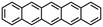
Picene |
| Formula |
C18H12 |
C20H12 |
C22H14 |
| Structure |

|

|

|
| Molecular weight/g mol−1 |
228.29 |
252.31 |
278.35 |
| Crystal structure |
Triclinic P![[1 with combining macron]](https://www.rsc.org/images/entities/char_0031_0304.gif) 31 31 |
Monoclinic P21/c32 |
Monoclinic P2133 |
|
a: 0.798 nm |
a: 1.0270 nm |
a: 0.8408 nm |
|
b: 0.614 nm |
b: 1.0839 nm |
b: 0.6082 nm |
|
c: 1.357 nm |
c: 1.1278 nm |
c: 1.3429 nm |
|
α: 101.3° |
α: 90° |
α: 90° |
|
β: 113.2° |
β: 101° |
β: 90.023° |
|
γ: 87.5° |
γ: 90° |
γ: 90° |
| Number of molecules Z |
2 |
2 |
2 |
| Surface index |
(001) or (00) |
Not specified |
(001) |
| Discussed in |
Section III.1.(2). |
Section III.1.(5). |
Section III.1.(4). |
| Pentacene |
Perfluoropentacene |
Rubrene |
C60 |
| C22H14 |
C22F14 |
C42H28 |
C60 |
|
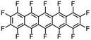
|

|

|
| 278.35 |
530.22 |
532.67 |
720.64 |
| Triclinic P34 |
Monoclinic P21/c35 |
Orthorhombic Cmca36 |
Cubic Fm![[3 with combining macron]](https://www.rsc.org/images/entities/char_0033_0304.gif) 37 37 |
|
a: 0.6266 nm |
a: 1.551 nm |
a: 2.686 nm |
a: 1.426 nm |
|
b: 0.7775 nm |
b: 0.4490 nm |
b: 0.7193 nm |
b: 1.426 nm |
|
c: 1.4530 nm |
c: 1.1449 nm |
c: 1.4433 nm |
c: 1.426 nm |
|
α: 76.475° |
α: 90° |
α: 90° |
α: 90° |
|
β: 87.682° |
β: 91.567° |
β: 90° |
β: 90° |
|
γ: 84.684° |
γ: 90° |
γ: 90° |
γ: 90° |
| 2 |
2 |
2 |
4 |
| (001) or (00) |
(100) |
(100) |
(111) |
| Sections III.1.(3) and III.2.(2). |
Section III.2.(3). |
Section III.1.(1). |
Section III.2.(1). |
II. Theoretical fundamentals of photoelectron spectra
In this section we describe briefly theoretical bases of photoelectron spectra of crystals using some approximations at zero temperature. Explanations are mainly for helping researchers in experimental fields and non-experts of photoelectron spectroscopy to understand this article. A very primitive “getting started” guide for the ARUPS methodology on organic semiconductor single crystals is given in Sections II.11 and II.12.
1. Electron–photon interaction Hamiltonian and photoionization of solid
The total Hamiltonian H for the electron system of a crystal in the presence of external electromagnetic field is given by the following eqn (1) using the Hamiltonian of an N-electrons system He without the electromagnetic field, the Hamiltonian of the electromagnetic field Hrad, and the Hamiltonian of moving electrons in the electromagnetic field He,rad. Here we use “rad” to specify the Hamiltonians, which involve effects of the electromagnetic field, as we will discuss ionization of a crystal by an electromagnetic radiation.| | 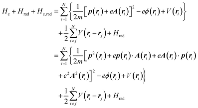 | (1) |
where m and −e is the electron mass and charge, respectively, A the vector potential of the electromagnetic field, ϕ(r) the static potential of the electromagnetic field,  represents the potential energies of electrons without electron–electron interaction, and
  the potential energies of the interacting N-electrons in the crystal. Hereafter we omit summation for N electrons in the crystal (p1, p2,…, pN; r1, r2,…,rN) for simplicity and describe the potential energy terms with V. We chose ϕ(ri) = 0 from possible selection of gauge function for zero current and charge system, put p·A = 0 by neglecting strong surface induced phenomena and furthermore neglect A2 term which is much smaller than the p·A term, giving
| |  | (2a) |
| |  | (2b) |
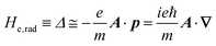
| |  | (2c) |
The interaction Hamiltonian He,rad changes both of the electronic states [eqn (2a)] and the radiation (photon) states [eqn (2c)]. The vector potential is written using a complex form of A, as  for ℏωkp photons because of a mathematical convenience. For radiations of various ℏωkp, the vector potential is rewritten, because it is real quantity, as
| |  | (3) |
where ekpγ (γ = 1, 2 denotes the polarization of the photon) are unit vectors which are orthogonal to each other and describe any direction of the A vector on the plane perpendicular to the direction of the photon momentum ℏkp. For this equation, V means the volume of the system. For a straightforward view of the photon absorption by the electron–photon interaction, we use the second quantization method for the electromagnetic radiation. We thus introduce one-photon creation  and annihilation (akpγ) operator and describe Hrad as given in eqn (2c).38 The operators
  and akpγ are directly related to the vector potential A of the radiation in a crystal with an ωkp- and kp-dependent dielectric constant [εr(ωkp,kp)] as
| |  | (4a) |
| |  | (4b) |
Using  and akpγ, He,rad is given as
| | 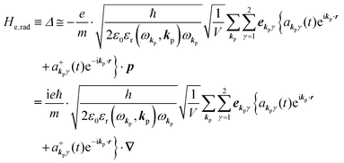 | (5) |
where ekpγeikp·r·∇ operates on the eigenfunction of the electronic states, while ekpγakpγeikp·r and  operate on the eigenfunction of the radiation. Hereafter we use the dipole approximation, eikp·r ≅ 1, and write unperturbed Hamiltonians for the electron and the photon system as H0e and H0rad, respectively, in the following discussion.
2. Dielectric screening effects at photoionization and its impact on ARUPS
In many books and papers, εr = 1 or constant are assumed in describing photoionization of solid. We here notice that we cannot assume constant value for εr but should use ωkp- and kp-dependent εr because phenomenon such as the multi-atom resonant photoemission (MARPE) takes place and dynamically screens the effective interaction between the incidence photons and electrons that are photo-emitted.39,40 When such transitions, ionization and bound-states transition, occur resonantly, the result is phenomenologically equal to ionization at decreased ionization probability at a specific photon energy. Therefore, we here use ε0εr(ωkp,kp) in eqn (4) and (5) instead of the vacuum permittivity ε0, as we need to measure the photon energy dependence of the spectra for measuring band dispersion along surface normal direction and photoelectron yield spectra. Both results require qualitative information of the screening for meaningful data analyses.
3. Description of photoelectron spectra: an electron excitation upon annihilation of single photon
For unperturbed systems we write the ground state (initial state of photoionization) of N electron system by using Ψi(N) and the final state of the ionization by Ψf(N), and that of the radiation consisting of photons with various wave vector kp and the polarization index γ (total photon number is  at unit volume) by |n11, n12, n21, n22,…,nkpγ,…〉, where the total photon number is
  at unit volume and we write this as
  in the following equations. These unperturbed systems and the non-interacting electrons-and-photon coexisting system satisfy following equations:
| | 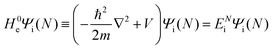 | (6a) |
| | 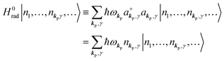 | (6b) |
| |  | (6c) |
When the electrons and the photons interact through the interaction Hamiltonian in eqn (2b), both of electrons and photons states change upon absorption of the single ℏωkp photon by exciting one electron to an exited state. The final state of these changes involves the ionized crystal with (N − 1) electrons, one photoelectron and (n1,…, nkpγ − 1,…) photons, and is thus described as |Ψf(N)〉 |n1,…, nkpγ − 1,…〉. Then transition rate (wif) from the ground (initial) state of the N-electrons and the radiation system to the photoionized (final) state upon absorption of an ℏωkp photon is written by using the Fermi's golden rule and eqn (4)–(6) as| | 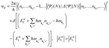 | (7) |
The photoelectron spectrum [I(E)] observes electrons photoexcited from various levels (also use i for various initial state i). I(E) is described as| |  | (8) |
As photoelectron spectroscopy utilizes a monochromatic radiation, we here consider only mono-energetic photons, which are specified with photon energy ℏωkp, photon momentum ℏkp, and photon numbers nkp. Then eqn (7) and (8) become to the following equation by choosing a convenient photon polarization (ekp).| | 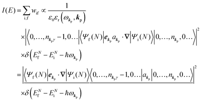 | (9) |
The first underlined part describes the one-electron transition/ionization matrix element by absorption of single ℏωkp photon and the second underlined part indicates that the initial number of ℏωkp photon, nkp, decreases to (nkp − 1) due to the excitation of an electron in the N-electrons ground state [Ψi(N)] to the excited N-electrons state [Ψf(N)]. The δ function describes the energy conservation of this process. Note that k conservation is also required but is not explicitly written here to simplify the equation.
If the initial state consists of excited electrons, an electronic transition to a lower energy level occurs through emission of an ℏωkp photon. For this photon emission process we use the photon creation operator  and thus the final state becomes |Ψf(N)〉|0,…, nkpγ + 1, 0…〉.
As 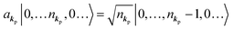 , we obtain following relation for the total photon number
| | 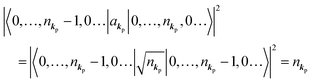 | (10) |
Therefore photoelectron spectrum becomes to
| | 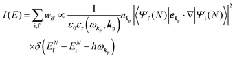 | (11) |
where
ENf involves kinetic energy of the photoelectron and the other energies associated with various excitations such as shake-up electrons, phonons, and other electronic correlation effects after removal of an electron from a crystal.
Eqn (11) indicates that
I(
E) and
wif is proportional to the initial photon number and |〈
Ψf(
N)|
ekp·∇|
Ψi(
N)〉|
2δ(
ENf −
ENi − ℏ
ωkp). Note again that the intensity of the radiation in a solid decreases by the dynamical screening effects by [
εr(
ωkp,
kp)]
−1 [see
eqn (5)] near specific
ωkp values. The dynamical screening may appear at the photon energies of anomalous dispersion regions of the dielectric function, and therefore may impact the band dispersion measured by sweeping photon energy of the incidence radiation. Contribution of the
εr(
ωkp,
kp) screening is also expected for photoelectron yield spectra, where the incidence photon energy is tuned in UV region which is in general anomalous dispersion region of materials, where ionizations and transitions to bound states coexist.
As it is easily convinced that full computations of Ψf(N) and wif are very difficult at present, various approximations are therefore utilized to estimate wif for understanding observed photoelectron spectra. Theoretical descriptions kinder to experimental researchers as well as progress of theoretical methods are essential to reach more quantitative understanding of electronic, optical and magnetic properties of molecular solids. There is a nice paper by Moser for experimental people to learn step-by-step the approximation levels of theoretical methods for photoelectron spectra of organic molecular solids.41
As a convenient approximation for understanding the origin of spectral features, experimental people generally use the three-step model42,43 of photoelectron emission based on the sudden approximation and one-electron approximation for photoionization of weakly interacting many-electron system.41,44,45 Within this approximation we describe Ψi(N) and Ψf(N) as
| |  | (12a) |
| |  | (12b) |
where

is the initial
j-th one-electron band specified by the electron momentum ℏ
kj or the initial
j-th molecular orbital (MO) level specified by a set of atomic orbital coefficients that corresponds to the
kj value,
46–48 from which the photoelectron is excited.
ΨRi,j(
N − 1) is the residual (
N − 1) electron wave function after separation of the
j-th state

as written in
eqn (12a),
C an antisymmetric operator which antisymmetrizes the
N-electron wave function, and i stands for initial state and R for remaining (
N − 1) electrons.

is the wave function of the photoelectron of momentum ℏ
kf, which is similar to the time-inverted wave function of low-enrgy electron diffraction (LEED) with the scattering state boundary condition
49,50 and
ΨRf(
N − 1) the wave function of the remaining (
N − 1) electron final state. Both of
ΨRi,j(
N − 1) and
ΨRf(
N − 1) are not expressed by one-electron wave functions as there are electronic interaction (correlation) in residual (
N − 1) electrons system. The structure of
ΨRi,j(
N − 1) depends on

, and
ΨRf(
N − 1) should have large impacts of photogenerated “hole” and therefore involves unknown energetic excitation such as creation of phonons, polarons, and changes in other electronic energies after the hole creation. Therefore
ΨRi,j(
N − 1) and
ΨRf(
N − 1) are in general discussed based on many-particle theory.
38,41,44 Here we consider such various states for
ΨRf(
N − 1) specified formally by
s. We then write
| |  | (13) |
Accordingly the transition probability
wif, which determines the photoelectron energy distribution
I(
E), is written as
| |  | (14) |
where
Mif is the one electron dipole-transition matrix element for i → f transition and
A(
k,
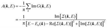
E) is so called one-electron spectral function
38,41,44 or spectral density function,
51,52 which are defined respectively as
| |  | (15a) |
| | 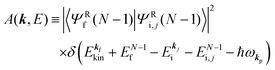 | (15b) |
In
eqn (15b) we omit
s thus

for simplicity till they become necessary.
A(
k,
E) describes energy and
k dependent density-of-stales [
ρ(
E,
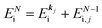
k)] owing to electron correlation, which will be discussed later again. Here and after we use following symbols for the initial (i) and the final (f) state related electron energies:
(1)  , where
  and EN−1f are the photoelectron kinetic energy and the remaining (N − 1) electrons energy, respectively;
(2)  , where
  and EN−1i,j are the Hartree–Fock orbital energy of the j-th state or at momentun ℏkj of the j-th band and the energy of the remaining (N − 1) electrons at the absence of the one j-th state electron, respectively;
(3)  , where ΔEcorr,s (≡ ΔEcorr) is the correlation energy; and
(4)  , where
  is the binding energy of the j-th level or the j-th band at momentun kj.
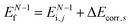
These energies are schematically shown in Fig. 1 for a very small band-dispersion system, where kj is read as j.
 |
| | Fig. 1 An example of effects of electron correlation in a molecular crystal with N electrons system and very small band dispersion. The occupied levels are shown like molecular orbital (MO) levels as the band dispersion is very small, therefore kj ≡ j. (a) Hartree–Fock (HF) ground state energy levels with photon ℏω before photoionization. (b1) The energy levels after a photoionization of the j-th level (thus (N − 1) electron system) and one photoelectron. (b2) The energy levels of (N − 1) electrons system with energy-level shifts by electron correlation (ΔEcorr), where the correlation effects are described using the self-energy (Σ(k,E) = Re[Σ(k,E)] + i![[thin space (1/6-em)]](https://www.rsc.org/images/entities/char_2009.gif) Im[Σ(k,E)]) (see Section II.4). The real part (Re[Σ(k,E)]) of Σ(k,E) shifts the energy position (≡ ΔEcorr) and the imaginary part of Σ(k,E) broadens the energy levels after one electron removal. In (b2) the photoelectron has electron–phonon coupling (shown using excitations of molecular vibration), but broadening of the sharp vibration features change to a skewed curve with a peak at a lower kinetic energy (marked with red-color triangle). This type of correlation effects showing electron–phonon coupling in HOMO of molecular system is shown in Fig. 2. Im[Σ(k,E)]) (see Section II.4). The real part (Re[Σ(k,E)]) of Σ(k,E) shifts the energy position (≡ ΔEcorr) and the imaginary part of Σ(k,E) broadens the energy levels after one electron removal. In (b2) the photoelectron has electron–phonon coupling (shown using excitations of molecular vibration), but broadening of the sharp vibration features change to a skewed curve with a peak at a lower kinetic energy (marked with red-color triangle). This type of correlation effects showing electron–phonon coupling in HOMO of molecular system is shown in Fig. 2. | |
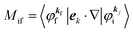
4. Meaning of one-electron transition matrix element and approximation methods
It is important to notice that the energy separation between upper occupied levels in the ground state of a weakly interacting organic molecular crystal, for example the energy separation between the highest occupied molecular orbital (HOMO) and the next highest occupied molecular orbital (HOMO−1) is in general much larger than not only energies of nonlocal crystal phonons but also energies of local phonons of light elements such as C–H stretching mode of molecular vibrations. In this case we can assume Mif = constant for photoelectrons in related satellite peaks (local phonons/molecular vibrations), tail features (nonlocal crystal phonons) of the main peak. In other words, we assume that Mif does not depend on the contribution of energy and momentum dependencies of 〈ΨRf(N − 1)|ΨRi,j(N − 1)〉 (see Fig. 2, 3(c), and 4), as full computation of Mif including effects of the electronic correlation (e.g. phonons, polarons, and so on) is still very hard for solids at present. The typical correlation effects are schematically shown in Fig. 1, where we use the complex self-energy (Σ = ReΣ + iImΣ) instead of ΔEcorr (Fig. 3(c) and 4).
 |
| | Fig. 2 HeIα UPS spectra for various phases of pentacene, showing an example of correlation effects. (a) Gas-phase at 433 K (black curve) reported by Kera and Ueno30 and at 508 K (red curve) by Coropceanu et al.53 (b) Lying-monolayer (1 ML) on HOPG (295 K, RT) from ref. 54, (c) 1 ML on HOPG (49 K, LT) from ref. 54, (d) standing-disorder ML film (1 nm) on SiO2 (295 K) from the same sample of ref. 55, and (e) standing-crystalline ML film (1.5 nm) on CuPc/GeS (295 K) from the same sample of ref. 55. All spectra are recorded by the same electron energy analyzer and UV lamp. The angle-integrated spectra are shown for the films after subtracting the background signals. The gas-phase ionization energy (IE) of 6.58 eV in ref. 55 is slightly different from the value (IE = 6.61 eV) in ref. 30. The abscissa is aligned to 0–0 transition peak in the gas-phase spectrum. IE for each film [(0–0) peak energy for sharp spectra and onset energy at the dashed line for film spectra] is described in the figure. Reproduced from ref. 30 with permission (Copyright 2015, Elsevier B.V.). | |
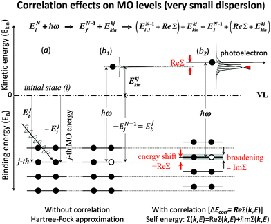
 |
| | Fig. 3 Angle-resolved photoelectron spectroscopy: (a) geometry of an experiment in which the emission direction of the photoelectron is specified by the polar (θ) and azimuthal (ϕ) angles; (b) momentum-resolved one-electron removal (photoelectron) and addition (inverse photoelectron) spectra for a noninteracting electron system (ca. metal) with a single energy band dispersing across the Fermi level EF; (c) the same spectra for an interacting Fermi-liquid system.56 For both non-interacting and interacting systems the corresponding ground state (T = 0 K) momentum distribution function [denoted as n(k) in this image] is also shown. Please refer original paper for the n(k) jump, Zk, in the upper right in (c). (c) Lower right, photoelectron spectrum of gaseous hydrogen and the spectrum of solid hydrogen developed from the gaseous one.56 Reproduced from ref. 45 with permission (Copyright 2003, American Physical Society). | |
 |
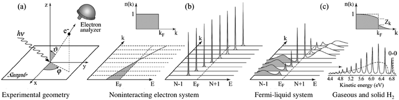
| | Fig. 4 Contribution of the self-energy to observed ARUPS spectra. (a) Schematic relationship between an observed energy band dispersion and Re[Σ(k,E)] and Im[Σ(k,E)]. If the band dispersion of the non-interacting case is known (or reasonably assumed) we can experimentaly determine Re[Σ(k,E)] and Im[Σ(k,E)] as shown schematically. (b) Theoretical results of the spectral function, A(k,E), for a one-dimensional model array of organic semiconductor molecule, where Ω0 in the figure correspond to an intramolecular deformation (vibration) energy.57 The first ARUPS results of an organic semiconductor (rubrene) single crystal is discussed in Section III.1.(6). Panel (b) is reproduced from ref. 57 with permission (Copyright 2011, American Physical Society). | |
5. Electron system without electronic correlation
For a system without electronic correlation, we can use following relation and therefore consider only the transition matrix element Mif.| | | 〈ΨRf(N − 1)|ΨRi(N − 1)〉 = 1 | (16) |
For this simple case, we approximate wif in eqn (14) by the following relation by using ERf,s = ERi,j-th in eqn (15a) (ΔEcorr,s = 0), allowing very sharp theoretical spectral peaks represented with δ functions for relevant energy bands/levels ( ) [see Fig. 1(a, b1) and 3(b)],
| |  | (17) |
where  is the kinetic energy of photoelectron and
  the one electron Hartree–Fock energy of the initial j-th state
  , both of which refer the vacuum level here.
  is equal to the binding energy
  measured from the vacuum level (see Fig. 1), as we assume that the other Hartree–Fock orbitals do not change upon photohole creation at
  and there is no electronic correlation (the Koopman's theorem58,59). It is of note again that the photoexcitation of the electron must satisfy k conservation, although it is not explicitly written in eqn (17). This offers a simple picture to photoelectron spectra, where peaks observed in a photoelectron spectrum originate from electrons in the orbital/band
  at the binding energy
  . In other words, ‘they’ are photoexcited to the continuum state
  to emit a photoelectron with the kinetic energy of
  , and therefore eqn (17) tells that the photoelectron peaks offer a set of energies of occupied levels [see Fig. 1 and 3(b)].
For the one-electron j-th energy band, where the initial-state binding energy depends on the electron momentum ℏkj,†46–48 we observe a sharp peak moving on the binding energy scale as a function of kj because of both energy and momentum conservations as shown in Fig. 3(b) (i.e., noninteracting particle picture). The dispersion relation of the j-th band is thus obtained from the observed ARUPS spectra using the relation 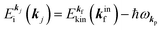 and using the momentum conservation of the photon and electron system inside of the crystal,
where
kinf is the photoelectron wave vector in the crystal,
kj the initial state wave vector,
kp the incidence photon wave vector, and
G the reciprocal lattice vector. As
kp is in general much smaller than the electron wave vectors
kinf,
kj, and
G, one can use
kp ≃ 0. We will discuss in Section II.10 accuracy of neglecting
kp in the above momentum conservation in organic molecular crystals, which generally have a small Brillouin zone (BZ) size due to large lattice constants resulted by a large molecular size.
6. Factors determining the spectral profiles
(A) The plane wave approximation for the photoelectron and its benefit.
Eqn (17) may be further approximated by using a plane wave for the final state as  .60,61 One needs to recall that a photoelectron travels at least in the attractive force produced by the Coulomb potential of the photogenerated ion/hole, and therefore its wavefunction cannot be described with a plane wave, as the plane wave is an eigenfunction of a free electron moving in ‘vacuum’. In order to describe the photoelectron inside and outside of a solid, the above eikf·r is modified to involve spherical waves produced by scattering with various Coulomb potentials inside and outside of the solid. The correct photoelectron wave function then reaches eikf·r at r → ∞, at which the Coulomb potentials become zero. As the use of a plane wave for
  does not impact photoelectron kinetic energy with respect to the vacuum level (defined at r → ∞), it is possible to discuss about results based on the energy conservation of photoemission but not possible to discuss intensity related phenomena because the phase of the photoelectron wave does change due to the scattering and interference effects thus impact on the intensity. The use of incorrect photoelectron wave function leads wrong results of angular distribution of photoelectron. However, the use of the plane-wave approximation can offer a large benefit for direct understanding of what photoelectron spectroscopy offers to us, if one does not discuss the spectral intensity and its angular distribution at high accuracy. The photoelectron spectrum I(E) becomes at the plane wave approximation to
| | 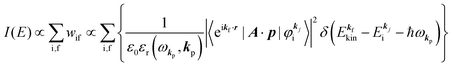 | (19) |
It was demonstrated for molecular solid systems, which consist mainly of light elements, that the independent atomic center (IAC) approximation,62–66 single scattering approximation,66,67 and even the simplest plane-wave approximation works reasonably well for discussing angular distribution of photoelectrons.68–70 Interestingly under the specific measurement condition with A·p ≈ constant, the observed photoelectron angular dependence [I(θ,ϕ)] from a dispersion-less molecular orbital [φi(r)] is proportional to its Fourier transform [|![[small variant phi, Greek, tilde]](https://www.rsc.org/images/entities/i_char_e12c.gif) i(k)|] at the plane wave approximation as described below,68
i(k)|] at the plane wave approximation as described below,68| | 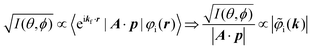 | (20) |
This in turn indicates, therefore, that the Fourier transform of the angular pattern of photoelectron spectrum can map a molecular orbital (MO) [φi(r)] by Fourier transform of  . This method is known as molecular orbital tomography for direct mapping of un-visible molecular wave functions using ARUPS.68,69,71 It is of note that the phase symmetry of MO was also measured by using circular polarization of incidence photons,70 although the phase information of the MO disappears by photoelectron spectroscopy measurements using linearly polarized photon because the spectrum is given by the square of the transition matrix element (|Mif|2).
(B) Spectral function with electronic correlation: impact of electron–phonon coupling.
When there is electronic correlation, it is necessary to discuss contribution of 〈ΨRf(N − 1)|ΨRi(N − 1)〉 in A(k,E) in eqn (15b) to the electronic density-of-state. For this discussion it is necessary to use a method of many-particle theory.38,51,52 According to the nomenclature of second quantization in many-particle theory, photoelectron spectrum, I(E), is written as following equation using electron creation (c+k) and annihilation (ck) operator, which are defined for a complete othonormal function system of unperturbed initial states (φ0i). As the transition matrix elements in the second quantization method is written as 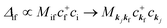 , at conservation of the wavevector upon i (the initial kj state) → f (the final kf state) transition with kj = kf,
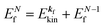
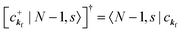
| |  | (21) |
where 〈N − 1,s;kf| is the N electron final state, which consists of (N − 1) electrons final state at an excited state specified by s and the one photoelectron with wave vector kf, |N,0〉 the N electrons initial ground state,  and ckf the one electron creation and annihilation operator with the wave vector kf, respectively, and so on. Here
  runs over the first Brillouin zone with momentum conservation kj (the j-th orbital/band of the initial state) = kf (the final state). Subscripts f and i of the energies in δ function are read as kf and kj, respectively, if necessary, or kf and kj may be replaced by f (final state) and i (initial state) for simplicity. We then rewrite eqn (21) to have following relation,
| | 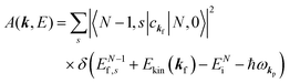 | (22) |
where ENf = Ekin(kf) + EN−1f,s and  . We used following relations to relate with the writing method before this section,
|Ψi(N)〉 ≡ |N,0〉 (initial ground state of interacting N electrons)
c
k
j
|N,0〉 = |N − 1, 0; kj = 0〉 (one electron with kj is extracted)
 (one electron with kj is added)
Then we can write as
| | 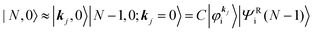 | (23a) |
and
| |  | (23b) |
where the underlined parts in
eqn (23b) mean a presence of one photoelectron with the wave vector
kf, and “≈” in
eqn (23a) and (23b) indicates the sudden approximation where the
kj electron |
kj,0〉 and the photoelectron |
kf〉 do not interact with the remaining (
N − 1) electron systems |
N − 1, 0;
kj = 0〉 and |
N − 1,
s;
kf = 0〉, respectively. When we simply write |
N − 1,
s;
kf = 0〉 as |
N − 1,
s〉, we have
| |  | (24) |
(C) Method of obtaining spectral function: Green's function and brief introduction.
For the electron interacting system, the spectral function A(k,E) is given by using the Green's function G(k,E) as| | 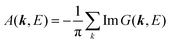 | (25) |
We can reach formally G(k,E) by the perturbation expansion starting from the non-interacting Green's function G0(k,E) of non-interacting (unperturbed) N-electron system described with H0φ0i = Ei0φ0i, where k is an index for the occupied single electron state (brief explanation and meaning of G0 and G are given in Appendix A).38,51,52
When we write the perturbation term due to the electronic correlation (H′) for a many-electrons system with Hamiltonian (H = H0 + H′) as H′ = Σ(k,E), we have,
| |  | (26) |
where
Σ(
k,
E) is an unknown complex function called self-energy. We generally write
Σ(
k,
E) using its real and imaginary part as
Σ(
k,
E) = Re[
Σ(
k,
E)] + i
Im[
Σ(
k,
E)]. Then the spectral function in
eqn (15b) is written using
eqn (25) and (26) as
| |  | (27) |
This shows that (i) the real part of the self-energy, Re[
Σ(
k,
E)], renormalizes the peak position from
E0(
k) to (
E0(
k) + Re[
Σ(
k,
E)]) because of formation of the quasi-particle/dressed-electron with energy difference, Re[
Σ(
k,
E)], from the dress-less electron due to electronic correlation, and (ii) the imaginary part, Im[
Σ(
k,
E)], describes its lifetime effect and thus gives a life-time broadening of the quasi-particle peak.
It is also convinced that Σ(k,E) is formally defined as
| | 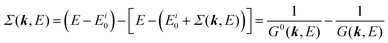 | (28) |
where
G(
k,
E) is approximately described with the Green's function for a non-interacting system
G0(
k,
E), indicating
Σ(
k,
E) may be calculated approximately based on results of non-interacting system (see Appendix A).
Using ARUPS, we can directly observe A(k,E), and therefore Σ(k,E) (see Fig. 4). Direct experimental measurements of Σ(k,E) for the HOMO band of organic semiconductor has been one of the most important challenges, which has been realized recently for rubrene single crystals72 as introduced in the Section III.1.(1). Depending on materials, namely Σ(k,E), we may observe a kink future and if phonon energy is large enough like ![[double bond splayed left]](https://www.rsc.org/images/entities/char_e009.gif) C–H stretching vibration in organics a gap future in the dispersion curve [see Section III.1.(1)].
C–H stretching vibration in organics a gap future in the dispersion curve [see Section III.1.(1)].
As discussion of the observed spectra requires some knowledge of many-body theory, namely, nomenclature of the second quantization and Green's function method, we recommend readers from chemistry field, in particular working in experimental field, to refer books and articles which introduce such methods of mathematical science.
7. Effective mass of the charge carrier
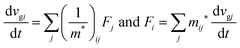
When we consider the transport of charge carriers in semiconductors, we need to discuss the carrier motion in the framework of the energy band theory, where effects of the crystal potential are involved in the effective mass m* of the traveling charge carriers. Therefore we discuss their motion in relation to a motion of a classical particle with m*. Under the classical Drude model,73m* is directly linked to the charge carrier mobility μ as μ = qτ/m* where q and τ are the unit charge and relaxation time, respectively, of the carrier. This means that m* is a convincing index for judging an aptitude of the material for efficient electronic devices, or that acquaintance of both μ and m* leads to knowledge about τ of the material which represents loss-factors for the charge carrier conduction.
As a more accurate treatment for the charge carrier motion, Ehrenfest's theorem,74,75 which correlates quantum mechanics and Newton's equation of motion, gives the following relation,
| | 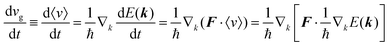 | (29) |
where
vg is the group velocity of the wave packet and 〈
v〉 [= ℏ
−1∇
kd
E(
k)] is the expectation value of the electron velocity in quantum mechanics and
F [= (d
E/d
t)(1/〈
v〉)] is external force other than the crystalline force associated with the periodic potential in a crystal. In this subsection,
i and
j are used as one of the Cartesian coordinates
x,
y, and
z. We have following relation for the
i-th component,
| | 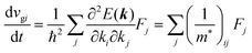 | (30) |
and
| |  | (31) |
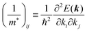
Here (1/
m*)
ij is the reciprocal effective mass tensor and
Fj is an external force acting on the electron along the
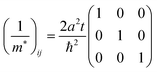
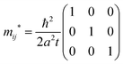
j-th coordinate in the crystal. The matrix of the effective mass tensor (
mij*) is given by the inverse matrix of the reciprocal effective mass tensor, (((1/
m*)
ij)
−1), as
| | 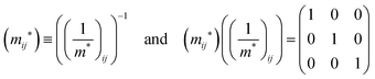 | (32) |
The
i-th component of the acceleration and the force vector, as examples, are written below using the reciprocal effective mass and the effective mass tensors, respectively.
| |  | (33) |
The crystal lattice can be aligned to the principal axis of the system. In this case its reciprocal lattice centers at the band extremum for many of organic crystals. If E = E(k) dispersion relation is parabolic at the extremum point, all off-diagonal terms in the reciprocal effective mass tensor [(1/m*)ij] and the effective mass tensor (mij*) vanish to have only diagonal terms. This means that if we assume parabolic dispersion near the bottom of the lowest unoccupied molecular orbital (LUMO) and the top of the highest occupied molecular orbital (HOMO) to define the effective mass of an electron (me*) and a hole (mh*), respectively, the effective masses become scalar. An example of concrete matrixes of (1/m*)ij and mij* are shown in Appendix B.
8. How to obtain the effective mass
For valence bands, which are experimentally measured with ARUPS, the spectra give information on one-hole states with effects of electronic correlation. Therefore, we generally say that photoelectron spectroscopy is looking at the hole bands (one-hole states with electronic correlation effects), while inverse photoelectron spectroscopy (IPES) gives information of the electron bands (one electron state with electronic correlation effects). Here we describe the method of obtaining the hole-band dispersion and the effective mass of the hole from the experimental dispersion curve. The method also applies to the electron band determined by IPES and to the extraction of the electron effective mass. Because the holes, which are responsible for the hole transport, exist near the valence band maximum (VBM), we expand the valence band dispersion near the band top in a quadratic form of the momentum ℏk to relate the momentum in classical mechanics around this 3-D extremum position. Taylor's expansion of E = E(k) in the 3-D is written as shown below (for generality we write k giving the VBM as k0):| | 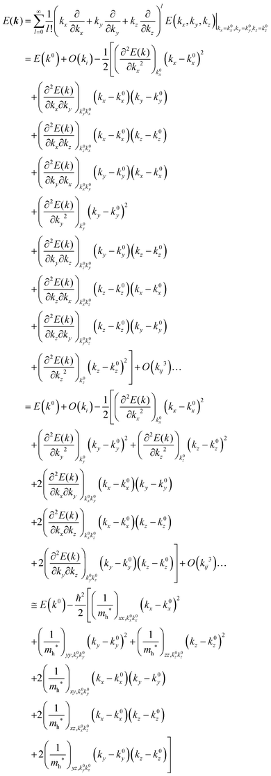 | (34) |
where the linear terms O(ki) is zero, and O(kij3) and higher order terms of k are neglected. We then obtain| |  | (35) |
Therefore for a system with k0i = k0j = 0, we have following equation,| |  | (36) |
For isotropic case and one-dimensional (1-D) case, we can use following relation near the extremum for the HOMO (hole) band.| |  | (37) |
9. How to extract the effective mass from experimental band-dispersion curve
(A) Tight-binding approximation.
In the case of many organic molecular crystals intermolecular interaction is not so strong that the band structure may be approximated with the tight-binding model. In this case the band dispersion is described using the band center energy, Ec, the transfer integral, t, and the related lattice constant (the periodicity length), a as| | | E(k) = Ec + 2tcos(ak) | (38a) |
| |  | (38b) |
Here we assume valence band maximum exists at Γ point, which is at k = k0 [k0 is given by k = 0 + nG, where n = 0, ±1, ±2, ±3,…, in the extended zone scheme and n = 0 in the reduced zone scheme] for simplicity. A hole contributing hole transport exists near the valence band maximum, thus its effective mass, mh*, is obtained as| |  | (39) |
For the three dimensional (3-D) simple cubic (SC) crystal with lattice constant a, s-band dispersion is written as,
| | | E(k) = Ec′ + 2t[cos(akx) + cos(aky) + cos(akz)] | (40a) |
| |  | (40b) |
The reciprocal effective mass tensor at the band maximum
kx =
ky =
kz = 0, (1/
m*)
ij, is given from
eqn (40b) as
| |  | (41) |
Thus the hole effective mass tensor,
mij* is isotropic and given as
| |  | (42) |
For the p-band, the dispersion is not isotropic because p atomic orbital
ϕp(
r) (thus π orbital) is not isotropic, resulting in the following dispersion for the Bloch state of
in SC, where
ϕpx(
r) ≡
ϕp(
r)
x and

is the normalization constant.
| | | Epx(k) = Ec′′ + 2t1cos(akx) + 2t2[cos(aky) + cos(akz)] | (43a) |
| | | ≈(Ec′′ + 2t1 + 4t2) − a2t1kx2 − a2t2(ky2 + kz2) | (43b) |
For
Epy(
k) and
Epx(
k) we also have anisotropic dispersion similarly (not shown). For
ky =
kz = 0,
Epx(
k) shows
Ec′′ + 2
t2 + 2
t1cos(
akx) dispersion along
kx, whereas for
kx =
kz = 0,
Epx(
k) →
Ec′′ + 2
t2 + 2
t2cos(
aky),
etc. In these cases, therefore, ARUPS can measure the cosine curves along the symmetry lines,
x,
y, and
z, with bandwidth of 4
t1, 4
t2, and 4
t2, respectively. Then we obtain the dispersion relation along the symmetry lines thus corresponding effective mass as the 1-D case. Care must be taken regarding the overall bandwidth, which is measured by angle-integrated UPS, as it is given by the energy difference of the maximum and the minimum values (4
t1 + 8
t2).
On the other hand, for lower symmetry crystal structures such as triclinic structure, where angles between the basic crystal axes (α, β, and γ) are not orthogonal, anisotropic dispersions become more complicated, producing more difficulty to obtain effective mass tensor components because of non-zero values of non-diagonal elements with crossing terms of the second-order partial differentiations (see matrix elements in Appendix B).
When the observed band dispersion is well approximated by the tight binding model along a symmetry direction, the effective mass of the hole that contributes to the hole transport along the direction in the surface parallel plane is obtained by following steps using ARUPS results by the photoelectron take-off angle dependence.
(i) fit a tight-binding energy-band dispersion curve of eqn (38a), (40a) and (43a) with the observed result to obtain t,
(i′) if a is unknown, one can also obtain a from the periodicity agreement between the cosine curve and the experimental dispersion curve measured over the Brillouin zone width (2π/a) using a as an adjustable parameter,76–78
(ii) the value of t is obtained from a quarter of the dispersion width (2t × 2),
(iii) calculate mh* using eqn (39) and values t and a after confirming the periodicity of the observed band dispersion being consistent with that expected from the value of a.
(iv) For the anisotropic case in cubic and orthorhombic crystals (α = β = γ = 90°), we can estimate t1 and t2 and mh* along the principal symmetry axes. For low-symmetry crystal structures with non-orthogonal unit cell axes one consider carefully the contribution of the off-diagonal terms of the effective mass tensor.
On the other hand, in the surface normal direction, the band dispersion and hole effective mass can be derived using the normal emission ARUPS spectra measured as a function of the excitation photon energy as described in Section II.10.78 For the crystals that have a band dispersion in the surface normal direction which is comparable to the surface parallel dispersion, one has to be careful to choose the photon energy and measurement geometry of the ARUPS analyses for minimizing impact of the surface normal dispersion onto the desired band structures along the surface parallel directions. One example for this situation is introduced in Section III.1.(6).
(B) Non-tight-binding case/purely experimental method.
As concept of the effective mass is based on the relation between the equation of motion of classical mechanics and corresponding description with quantum mechanics, the motion of an electron and a hole in a crystal can be discussed as a classical particle by replacing the mass in the Newton's equation of motion to the effective mass in a crystal potential. We therefore perform a parabolic curve fitting to the observed dispersion curve simply using mh* as fitting parameter (see Fig. 5). In this case it is strongly recommended to measure reasonable number of k points around the top of the HOMO band position (extremum point) to realize plausible mh* estimation. We then just apply the simplest 1-D parabolic curve fitting to the HOMO band maximum and fit the parabola curve with the E–k plot of ARUPS data points near the HOMO band maximum using mh* as a parameter. It is therefore recommended that one compares mh* estimated by using methods (A) and (B).
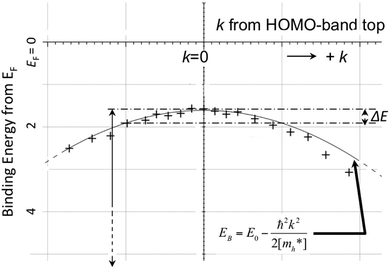 |
| | Fig. 5 Extraction of the effective mass from an experimental energy band dispersion curve. It is recommended to use ΔE ∼ 100 meV (∼4kBT where T ∼ room temperature). | |
It is also recommended from our experience of UPS that we should consider (i) the number of measurement points for a plausible mh* estimation, as the accuracy in determining a dispersion curve requires at least five points for energy width of 0.1 eV, ∼4kBT with T = room temperature, and (ii) organic systems are generally not durable against ionizing radiations even at low-energy vacuum ultraviolet (VUV) light such as HeIα (hν = 21.218 eV). The requirement (ii) pushes a researcher to choose a shorter signal accumulation time to obtain the results of damage-free sample, while (i) requires a longer measurement time or a worse energy and momentum resolution to increase photoelectron-collection sensitivity. Careful consideration on these points is always necessary prior to the measurements to realize meaningful measurements.
There are experimental parameters, namely photon energy, photon polarization, photoemission geometry, energy and angular resolution of the analyzer, S/N ratio of the spectra, characteristics of target sample such as its purity/quality and sample temperature, etc. In some cases, non-careful handling and rapid temperature change of the single crystals introduce unexpected defect states into the crystal, leading to difficulty of using photoconductivity in overcoming charging of the crystal during photoionization. We need to evaluate these experimental parameters and conditions, semi-quantitatively as possible as we can.
10.
k broadening due to short escape depth of photoelectron
In ARUPS measurements, there is an intrinsic uncertainty in measuring the photoelectron momentum perpendicular to the crystal surface due to a finite inelastic mean free path (escape depth) λ of the photoelectron.79,80 Here, we briefly describe the impact of λ to an uncertainty of the photoelectron momentum using 1-D case along the z-axis being taken perpendicular to the surface. Inside a crystal, the phenomenological intensity of photoelectrons at z [I(z)], which are photoexcited at z = 0, decays exponentially with z during traveling in the crystal. I(z) is given as| | 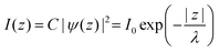 | (44) |
where C is constant and ψ(z) is the photoelectron wave function. Upon escape of photoelectron to vacuum through the surface, ψ(z) changes from the exponential-decay wave to a non-decay one (damping free), and the surface normal component of the electron momentum is altered as described in Section II.11. To simplify the complex mathematical procedure in Fourier transformation of ψ(z) involving such effects, we neglect the effects and use an exponentially damping plane wave for ψ(z) of an photoelectron kz0, and then we approximately obtain the Fourier transformation of ψ(z) for evaluation of the momentum broadening due to λ effects. We use a following ψ(z), which satisfies eqn (44).| |  | (45) |
where B is constant. One can easily obtain the Fourier transformation of ψ(z)[ψF(kz0)] as| |  | (46) |
Then the photoelectron intensity with kz0[I(kz0)], which is approximately given by |ψF(kz0)|2, becomes| | | I(kz0) ∼ |ψF(k)|2 = ψF(k)·ψF(k)* | (47) |
Eqn (47) shows that the momentum distribution of photoelectrons in the crystal is described by a Lorentzian function with the full width at half maximum (FWHM) of 1/λ. Note that the kz distribution is symmetric and its FWHM becomes 1/λ, although the intensity I(z) decreases to 1/e after traveling the distance of λ. It is thus convinced that the ARUPS spectral width in k space, namely uncertainty of kz (Δkz) may be given as Δkz ∼ λ−1. This result is obtained simply using the uncertainty relation, (Δz)·(Δpz) ≳ ℏ.‡74,81 When z ∼ λ, one obtains following result.| | 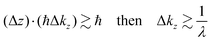 | (48) |
The above results indicate that photoelectron spectroscopy has a principal k-broadening effect due to amplitude damping of the wave function. The escape depth/mean free path becomes very small in particular for electrons excited by hν in VUV region as described in the next section. Therefore, one must always consider effects of the k-broadening as well as the photon momentum when selecting experimental conditions for the band dispersion measurements and discussion on measured results. With increase in the required precision and accuracy of the discussion, the Δkz problem as well as the photon momentum contribution should be considered more carefully. In particular for organic molecular crystals of large molecules, for instance, (i) the size of Brillouin zone becomes smaller with the molecular size, which requires small Δkz experimental condition, and (ii) in some molecular systems the bulk band structure measurement needs to use larger/smaller hν to realize large λ photoelectron spectroscopy (see Fig. 6).
 |
| | Fig. 6 Momentum of an electron and a photon as a function of the energy. The uncertainty of momentum normal to the surface Δkz originating from a spatial confinement due to restriction in the electron inelastic mean free path (IMFP)82 is also drawn as a thick light-gray curve. Brillouin zone sizes of some metal,83 semiconductor,84 and molecular crystals34,36,37 are also indicated for reference. | |
11. Simplified procedures for translation of the ARUPS spectra into the band structures
In the most simplified one electron model, the energy conservation relation during the photoelectron spectroscopy measurements is illustrated as Fig. 7. The energy conservation for the photoelectron spectroscopy measurements expressed as the δ function in eqn (9) can be written as;by simplification of ENf, ENi, and ℏωkp into Ef, Ei, and hν, respectively. For the first photoabsorption step within the three-step model framework for the photoemission process, the above equation can be rewritten as;where the final state energy Ef is approximated to be the kinetic energy of one photoelectron inside the solid Eink, and the initial state energy Ei corresponds to the ground state binding energy EB for this electron. Here refers the EF from the experimental requirement of an accurate electron energy measurement based on thermal equilibrium throughout the electron system of the specimen and the energy analyzer.§
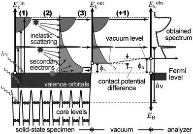 |
| | Fig. 7 Schematic drawings of the three-plus-one step model of the photoelectron spectroscopy indicating the energy conservation. | |
During the second step, some photoelectrons lose their kinetic energy by the inelastic scattering in the solid before reaching the surface. In other words, a number of photoelectrons that preserves their original energies attenuates as going deeper the source of the photoelectrons is. The electron inelastic mean free path (IMFP) λ determines the mean distance that the photoelectrons can migrate before experiencing the first inelastic scattering event, which strongly depends on Eink but is substantially independent of the materials. An empirical “universal curve” of the λ–Eink relationship is approximated to be λ ∝ E−2 and λ ∝ E+0.5 for E < 15 eV and E > 150 eV, respectively,82 and λ reaches its minimum in the intermediate energy region. As shown in Fig. 8(a), λ for molecular solids is less than 1 nm for the conditions in standard UPS measurements (typically hν > 20 eV),85,86 which restricts an accessible depth of UPS to at most single molecular length from the surface at the standing orientation.
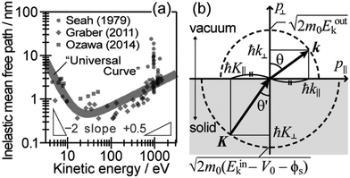 |
| | Fig. 8 (a) The “universal” relationship between the energy and inelastic mean free path λ of electrons in solids. The marks indicate individual experimental data of λ for organic solids. (b) Schematic drawing of momentum conservation for the ARUPS measurements. | |
In the third step, the surface potential decelerates the photoelectrons as;
| | | Eoutk = Eink − ϕs = −EB + hν − ϕs | (51) |
where
Eoutk is the kinetic energy of the photoelectron out of the solid and
ϕs is the work function (surface potential) of the sample. Only the photoelectron reaching the surface with a sufficient energy can escape out of the solid sample.
For practical measurements, flight of the emitted photoelectrons in a vacuum gap between the sample and an electron analyzer has to be taken into account as the plus-one step in addition to the above three. Since the work function of the electron analyzer ϕa is generally not equal to that of the sample ϕs, the external photoelectrons are further decelerated or accelerated by a contact potential difference (ϕa − ϕs) between the analyzer and sample during the flight through the vacuum gap in the fourth step. Altogether, the observed kinetic energy Eobsk of the photoelectron at the analyzer can be expressed as;
| | | Eobsk = Eoutk − (ϕa − ϕs) = −EB + hν − ϕa | (52) |
As explained in the previous section, the momentum of ultraviolet (UV) photons is negligibly small in comparison to the crystal momentum in standard organic semiconductor materials. Therefore, one can consider that the momentum of an internal photoelectron ℏK preserves that of the ground state in the matter as long as it has not experience a scattering event [hereafter, we describe the electron momentum before and after the escape through the surface as K (capital) and k (small), respectively]. In the third step of the photoemission, the photoelectron is subjected to a backward force originating from the surface potential when going out of the solid surface, which modulate the momentum of the photoelectron to ℏk (≠ ℏK) as illustrated in Fig. 8(b). Since this force works only in a direction perpendicular to the surface, the surface parallel components of the electron momentum are conserved. This results in a refraction of the photoelectrons across the surface. In this section, K and k are expressed as two-dimensional (2-D) vectors in a plane that contains the surface vector and the photoelectron progression vector as;
| |  | (53) |
where the subscripts ‖ and ⊥ indicate the surface parallel and normal components, respectively.
Since a photoelectron in vacuum can be regarded as a (nearly) free electron,¶ the kinetic energy Eoutk of a photoelectron just out of the surface is expressed as a function of the momentum k as;
| |  | (54) |
where
m0 is the electron rest mass. This leads to a relation as;
| |  | (55) |
where
θ is the electron emission angle from the surface normal. Also inside the solid, the photoelectron can be regarded as a quasi-free electron in the case that the kinetic energy is sufficiently large (typically
Eink > 10 eV). The dispersion relation between the energy
Eink and momentum
K in the crystal can be expressed as;
| |  | (56) |
where
E0 corresponds the bottom energy of this pseudo-parabolic dispersion relation with respect to the Fermi level. Whereas the effective mass of the electron in the solid sample
m* is generally not identical to the free electron mass,
m* =
m0 is assumed for simplicity hereafter in this subsection. Under this approximation, the photoelectron momentum inside the solid is written as;
| |  | (57) |
where
θ′ denotes the angle that the photoelectron incidents the surface measured with respect to the perpendicular direction.
The conservation of the surface parallel component instantaneously gives the following relation as;
| |  | (58) |
Substitution of the physical constants leads to a practical relation between
Eoutk (in eV),
θ, and
K‖ (in nm
−1) as;
| |  | (59) |
where
Eobsk ≈
Eoutk is generally approximated.
On the other hand, eqn (55), (57), and (58) lead to the refraction condition of the photoelectron across the surface as;
| |  | (60) |
Therefore, the surface normal component of the momentum is expressed as a function of
Eoutk as;
| |  | (61) |
where
V0 (≡ −
E0 +
ϕs > 0),
|| generally referred as the “inner potential”, corresponds to the depth of the pseudo-parabolic dispersion of the internal photoelectrons measured with respect to the vacuum level of the sample.
87,88 An ordinary method for obtaining an
E–
K⊥ dispersion relation is collecting the UPS spectra depending on the excitation photon energy
hν in the normal emission geometry (
θ = 0). For this condition,
K⊥ can be related to
Eobsk in the same manner to the case of
K‖ as;
| |  | (62) |
where the unit of
K⊥ is taken in nm
−1 and those of
Eoutk and
V0 are in eV. In most cases,
V0 is treated as a fitting parameter.
Based on above, the ARUPS, as a methodology of measuring the photoelectron Eobsk depending on θ at a certain hν, provides the experimental knowledge about the E–K dispersion relation of the crystalline samples. It has not to be overlooked that, as mentioned in Section II.8.(A), the parameter θ relates to both K‖ and K⊥; this means that the change of θ in the ARUPS experiments scans not simply in a K‖ direction but also shifts K⊥. In some cases, this situation leads to difficulty or errors in determination of the band energy at aiming K points when the sample crystal exhibits considerable energy dispersion also in the surface normal direction.
12. Method of overcoming sample charging of an electrical insulator upon photoelectron emission and experimental know-how
When one deduces the energy and momentum of electrons inside a solid sample from the observed kinetic energy Eobsk and momentum ℏk of the photoelectrons by the schemes described in the previous section, the following two conditions are implicitly hypothesized; the first one is alignment of the Fermi level between the surface of the sample and the electron analyzer, and the second is a robustness of the material, namely the physical/chemical conditions of the sample does not change throughout the duration of the photoemission experiments. For molecular solids, however, these two conditions are not always fulfilled. Violation of the latter condition is generally referred as “radiation damage” (or irradiation damage) of the sample. Photoelectron spectroscopy experiments apply an extra energy to the sample and generate photoelectrons and secondary electrons of excess energies inside the sample, which fundamentally involves a risk of triggering decomposition or polymerization of the consisting molecules (chemical changes) and in some cases induces a change in the molecular packing structure (physical effects). In order to avoid or ease this problem, reduction of the dosage of the excitation photons is a symptomatic but an effective treatment. For the laboratory sources (i.e., gas discharge lamps), attenuation of the irradiation intensity by inserting a polarizer and/or metal filter is a practical way. For the experiments using synchrotron orbital radiation, the excitation photon energy may be adequately selected to optimize the measurement condition. Especially for the undulator beamlines, the photon flux should be diminished by e.g. intentional sliding of the undulator gap width away from the optimized value.89 Another tactic against the radiation damage is a reduction of the excitation energy,90 which has recently achieved an impressive success as low-energy inverse photoemission spectroscopy (LEIPS).91 Although this is not an ultimate solution for the radiation damage problem, a usage of the characteristic radiation of e.g. Xe (8.437 eV for the Iα line**) instead of He (21.218 eV for the Iα line) may be a useful option in this course of direction in the case of the normal photoemission spectroscopy.
The former condition, the Fermi level alignment throughout the system, is also problematic for the organic semiconductor samples. This condition is fulfilled during the photoelectron spectroscopy measurements only in the case that a positive charge (photohole) left after a photoemission event is immediately cancelled out; in other words, the photoelectron spectroscopy measurements require the electric conductance of the sample to be sufficiently high. Otherwise, the Fermi level position (electrostatic potential) in the sample and at the surface is inhomogeneously modulated by localized photoholes, and the resulting electrostatic field perturbs the energies and momentums of successive photoelectrons. This obstruction is generally recognized as the sample charging problem. This problem must be overcome for conducting the ARUPS measurements for the organic semiconductor crystals because electric conductivity of the organic semiconductors is generally very low due to wide energy gap widths (typically 2–3 eV). Actually, these materials had better be regarded as insulators rather than “semiconductors” unless the charge carriers are intentionally generated by e.g. the photoexcitation or injection from an attached electrode.
One commonly adopted trick is a usage of ultra-thin (typically thinner than 10 nm) crystalline films rather than bulk crystal samples for effective transport of the photoholes to the metal substrate and/or for the sake of facilitating cancelation of the photoholes using electrons from the substrate by contraction of “the electron path” though the sample.78 In this course of the direction, Hasegawa and coworkers reported the first experimental evidence for the formation of the inter-molecular valence bands on a few molecular-thick crystalline layers of a semiconductor molecule bis-(1,2,5-thiadiazolo)-p-quinobis(1,3-dithiole) (BTQBT) by means of the excitation energy dependence of the normal emission UPS spectra.92 A series of the ARUPS works on pentacene ultra-thin films in various crystalline polymorphs is another successful example.93–98 In recent years, novel technologies for solution-based production of over-mm-wide molecularly-thin single crystalline films of high-mobility organic semiconductors have rapidly progressed.99–105 It should be noted that, as these monolayer single crystals are often placed on dielectric (insulating) substrates attached with source and drain electrodes for organic field effect transistor (OFET) devices, ARUPS analyses on such device structures need to use photocurrent flowing from these electrodes parallel to the dielectric substrate. It would be necessary to use microscopically patterned electrodes with an interdigitated array structure on the dielectric substrate for the photoemission analyses because the photoholes (i.e., the cancellation electrons) can hardly pass through the mm-scale bulk crystal in the lateral directions.106 Yet these should be promising next targets for the ARUPS analyses using a micro beam of excitation UV photons, while there have still not been any reports of successful valence band mapping on these materials.
For the photoelectron spectroscopy analyses on bulk insulator specimens, one has to explore another way. Whereas the neutralization of the photoholes by using an electron flood gun has been a widely adopted tactic for inorganic insulator materials,107,108 it is hardly applicable to the organic semiconductor samples because the electrons tend to bring about the chemical degradation in these materials as mentioned above. Zimmermann et al. attempted the ARUPS measurements on the single crystal perylene with a compensation of the photoholes by thermionic electrons from a LaB6 filament equipped nearby the crystal, which was not succeeded in obtaining reasonable ARUPS spectra.109 Another potential approach for relieving the photoholes is a usage of the photoconductivity. Sato and coworkers reported pioneering studies of the UPS measurements on single crystal samples of several kinds of aromatic hydrocarbon molecules under a white light illumination to generate the photocarriers and also a coverage of the crystal surface by a thin overlayer of Au to form an additional pathway for electrons.110,111 Afterwards, Vollmer et al., conducted UPS measurements on the single crystal pentacene under the illumination of a laser light (532 nm, 2.33 eV).112
It was firstly demonstrated that the valence band dispersion on the bulk molecular single crystal samples is accessible by ARUPS under a simultaneous illumination by a supplementary laser light.113 As seen in Fig. 9(a), a peak derived from the highest occupied states of the single crystal rubrene arouse in a binding energy range of 0.8–1.5 eV as increasing the power of the supplementary laser (405 nm, 3.06 eV), whereas no clear spectral components were resolved in that energy range without the laser light illumination. This means that the sample charging was successfully canceled when the supplementary light of a sufficient intensity was supplied to the sample. It is worth subjoined that any reasonable spectra were hardly obtained when the wave length of the supplementary laser was longer (445 nm, 2.79 eV) even though the intensity of the light was more intense [Fig. 9(b)]. Taking the “transport gap” width of the single crystal rubrene (2.8 eV114) into consideration, this result suggests that the energy of the supplementary photon has to be large enough for the photocarrier generation in order to cancel the sample charging. It should be noted that, in principle, an existence of such additional photocarriers should not be the necessary condition for cancelling the photo-holes left after the photoemission events because these in the valence band could pass through the molecular single crystal sample. In fact, it was reported that some individual single crystal samples—presumably of ideally high crystal qualities and good electric contacts with substrates—did allow successful photoemission measurements even without any supplementary laser light.115 This phenomenon can be physically understandable, because if there are no charge trapping states in the band bap, the photogenerated hole in the HOMO moves by the image force and finally reaches the conductive substrate. Nevertheless, in practice, the simultaneous illumination by a laser light of a sufficient photon energy for photocarrier generation is an effective methodology to resolve the sample charging problem on general molecular single crystal samples with a certain trap density for the photo-holes. A point to be aware for judging whether the sample charging takes place or not is that spectral distortion due to the sample charging occurs quite promptly and often saturates within a few minutes as exemplified in Fig. 10. In other words, even though one finds no change in the spectral profile/energy during continuous measurements, it does not at all guarantee that those spectra are free from the sample charging because standard photoemission measurements take several ten minutes. Instead, sharpness of the spectral features (e.g. valence bands, core levels, and secondary electron onsets) gives an indication for successful relief (or absence) of the sample charging. It should also be noted that the intensity of the supplementary laser light has to be sufficiently high but not to be too intense as it can damage the sample. Therefore, the laser light has to be adequately reduced in power and also defocused for moderating the power density as well as realizing uniform irradiation to the sample surface. Nevertheless, this laser-induced damage caused a difficulty for accessing the valence band structures for some specific species (e.g. bis(trifluoromethyl)-dimethyl-rubrene116).
 |
| | Fig. 9 (a) Evolution of normal emission UPS spectra taken on a rubrene single crystal sample depending on the power of the supplementary laser light. (b) Normal emission UPS spectra on a rubrene single crystal sample without (gray) and with the supplementary laser light of the wave length of 445 nm (blue) and 405 nm (violet). A spectrum obtained after long-term measurements under illumination of the 405 nm laser light is also plotted as a thin-broken curve. For this series of measurements, the sample was positively biased at +20 V for the sake of reducing the total photoemission amount.89 The original data of (a) are taken from ref. 113. | |
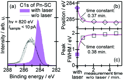 |
| | Fig. 10 (a) C1s XPS spectra sequentially measured on a pentacene single crystal sample; the first sweep under illumination of the supplementary laser light (405 nm, 30 mW) displayed as a shaded area and second to fifth sweeps without the laser light shown in thin lines. (b and c) Evolution of the peak position and broadness, respectively, of the C1s XPS spectra depending on time after turning off the supplementary laser light (time zero corresponds to the peak position and width under the laser light). The original data of (a) are taken from ref. 89. | |
Additionally, it has to be ensured that the crystal sample is in good electric contact with a conductive substrate (e.g., a piece of the Si wafer coated with Au) in order to avoid the sample charging. One effective style is to surround the crystal sample with a conductive glue (e.g., Ag paste) for bounding the sample onto the substrate as exemplified in Fig. 11. However, this manner of fixing the crystals tends to lead to a difficulty of changing the sample temperature due to significant mismatches of the thermal expansion coefficients between the inorganic substrates and the molecular crystals. A usage of a conductive adhesive tape (i.e., carbon tape) instead as a soft substrate can ease the mechanical strain and prevent a molecular crystal from cracking for low temperature experiments.117
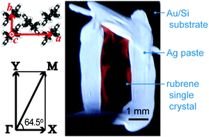 |
| | Fig. 11 Surface molecular arrangement, surface Brillouin zone,†† and typical sample appearance of the rubrene single crystal. | |
The organic semiconductor single crystals can mostly be produced by gas phase recrystallization techniques. Fig. 12 schematically shows an apparatus for production of molecular single crystal samples. Object molecules sublimed from their crude source placed in a quartz tube are conveyed by a stream of an inert carrier gas (e.g. purified N2) to a lower temperature zone at which the molecules cohere to form into its single crystal pieces. This methodology is generally known as a (horizontal) physical vapor transport (PVT) technique.118 Several parameters, e.g., sublimation rate (temperature at the source), temperature gradient, flow rate of the carrier gas, etc., have to be optimized to obtain the crystals of favorable shapes (generally wide and thin plate-shape) as many as possible. Generally, the crystals were individually taken out in the ambient atmosphere for further processing to be prepared as specimens for the photoemission experiments as described in the previous paragraph. For maintaining the crystals “intrinsic” by avoidance of the exposure to the ambient conditions,119,120 sample treatment in a glovebox directly connected with the PVT equipment, as illustrated in Fig. 12, is an efficient measure as discussed in Section III.1.(3).
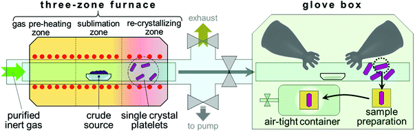 |
| | Fig. 12 Schematic drawing of an apparatus for production of molecular semiconductor single crystal samples with the clean surface. | |
III. Experimental results
1 Case studies
(1) Rubrene.
Rubrene, a derivative of tetracene [Section III.1.(2)] with four phenyl side groups, has been a benchmark material regarding charge carrier conduction in the organic semiconductor solids because of its outstanding transport characteristics of its single crystal phase. This molecule first attracted considerable attention because of a clear anisotropy as well as the magnitudes approaching 15 cm2 V−1 s−1 of the charge carrier mobility,121 and realization of the “band transport”, rather than the intermolecular hopping, was proved not only by temperature dependence of the charge carrier mobility122 but also by clear existence of the Hall effect.123,124 Moreover, this molecule had been a record holder of the mobility magnitude at RT among the molecular semiconductors.125 Because of such fascinating electric characters, the electronic properties, i.e., valence band structures, of the single crystal rubrene was of keen interests. Whereas theoretical calculations predicted a presence of widely dispersed valence bands,126,127 the experimental observation of the valence band structures by photoemission techniques was hindered by technical difficulties as described above. One successful example for probing the valence band properties with a photoemission technique of sample charging durability,128 that is photoelectron yield spectroscopy,129 however can hardly provide any indication about the E–K dispersion relation due to its angle-integrated nature of the technique.
Demonstration of the valence band dispersion of the rubrene single crystals by the ARUPS measurements was first succeeded with the excitation of the sample by the HeIα radiation (21.218 eV) under a simultaneous illumination by a supplementary laser light of a wave length of 405 nm (3.06 eV), as introduced in Section II.12.113Fig. 13(a) shows the ARUPS spectra of a rubrene single crystal sample taken approximately along the Γ–Y direction in the surface Brillouin zone (SBZ) which corresponds to the transversal direction of (typically) rectangular-shaped crystals of rubrene (see Fig. 11). The experimental geometry is illustrated in Fig. 13(b). While a peak in a BE range of 0.7–1.5 eV, which is attributed to the HOMO of rubrene, exhibited a right-weight profile for the normal emission (θ = 0°) spectrum, it transformed into a left-weight shape as inclining the emission angle θ. Further inclination of θ eventually reshaped the peak profile similar to that of the normal emission spectrum at θ ∼ 24°, which was followed by the second cycle of the peak transformation into the left-weight. This periodic trend represents a clear evidence for the presence of a notable energy dispersion in the valence band. Such spectral change was not observed for the longitudinal direction [Fig. 13(c)]. The series of the ARUPS spectra along Γ–Y can be mapped on a E–K‖ plane by translating θ into K‖ for each Eb using the eqn (57) and (58) as shown in Fig. 14(a), where the second-derivative of the photoemission intensity, rather than the “raw” intensity, is represented as a grayscale tone for highlighting the peak positions. This indicated that the periodicity of the variation in the HOMO peak position was actually consistent with the SBZ size in the Γ–Y direction. In Fig. 14(b), the BE positions of the HOMO peak in the 2nd BZ are plotted as a function of respective K‖. The E–K‖ dispersion relation derived from the present data agreed fairly well with a cosine curve under an assumption of the 1-D tight-binding (1D-TB) model.
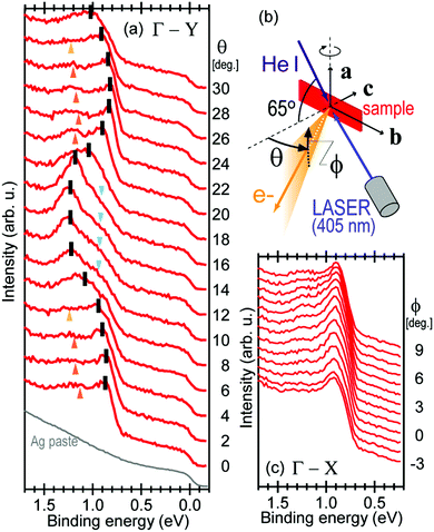 |
| | Fig. 13 (a) ARUPS spectra of a rubrene single crystal sample taken along the Γ–Y direction. The main peak position at each θ is marked with a thick bar, while the triangle marks indicate the shoulder components. The bottom curve represents a spectrum of the silver paste overlapping the rubrene spectra. (b) Schematic drawing of the experimental setup. (c) ARUPS spectra along the Γ–X direction taken on the same rubrene single crystal sample as (a). Reproduced from ref. 113 with permission (Copyright 2010, American Physical Society). | |
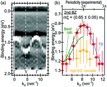 |
| | Fig. 14 (a) Second derivative of the ARUPS spectra mapped on the E–K‖ plane. (b) E–K‖ diagram of the main peaks along the Γ–Y direction in the second BZ. Theoretical curves by the band calculation and a 1D-TB fitting curve are also shown. Reproduced from ref. 113 with permission (Copyright 2010, American Physical Society). | |
In fact, the 1-D character of the valence band dispersion of the single crystal rubrene was confirmed by the ARUPS measurements to the three symmetry points of the SBZ (see Fig. 11).130 The ARUPS spectra in the Γ–X direction did not show any clear θ-dependence [Fig. 15(a)] whereas those taken along the perpendicular direction exhibited an evident θ-dependence [Fig. 15(b)] on the identical sample. In the diagonal direction of the SBZ (Γ–M), as shown in Fig. 15(c), the ARUPS spectra looked similar to those in the Γ–Y direction, whereas the periodicity of the dispersion relation was slightly extended reflecting a little wider distance to the BZ edge in the reciprocal space in comparison to the Γ–Y case. These results means that the valence band of rubrene exhibit a gutter-like shape in the SBZ. This strongly anisotropic character of the valence band was also pointed out by Ding et al. and later by Nitta et al.,131,132 whereas their ARUPS results failed to reproduce the valence band structure probably because of insufficiencies in the resolution of the data and/or in cancelation of the sample charging.‡‡ Vollmer and coworkers clearly demonstrated the anisotropic character by a 2-D mapping of the valence band using an angle-resolved time-of-flight (ARTOF) electron energy analyzer.§§133 In addition, unchanged HOMO peak ionization energy irrespective of the excitation photon energy [Fig. 15(d)] indicated that the valence band in the surface normal (Γ–Z) direction is flat due to a weak intermolecular interaction between the molecular layers (ab plane) in the single crystal rubrene.130 This substantially 1-D E–K dispersion relation of the valence band gives an electronic ground for a strong anisotropy of OFET devices of the single crystal rubrene so far reported.121 Actually, the intermolecular transfer integral for the HOMO orbitals, which can be derived from 2-D tight-binding (2D-TB) modeling of this valence band dispersion structures [Fig. 15(e–g)], has a significant value only along the most conductive b axis (which is parallel to the Γ–Y direction) whereas those in the perpendicular (a axis) and diagonal directions in the surface unit cell are substantially zero. This extreme anisotropy in t also rationalizes the working behaviors of the OFET devices based on this material.
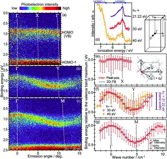 |
| | Fig. 15 (a–c) ARUPS spectra of a rubrene single crystal sample along the (a) Γ–X, (b) Γ–Y, and (c) Γ–M directions taken at the excitation energy of 30 eV. (d) Normal emission UPS spectra in the valence band region of the single crystal rubrene taken at various excitation energies. The horizontal scale is taken with respect to the vacuum level of each sample (corresponding to the ionization energy). The dots for the spectra for hν = 30 eV and 40 eV represent raw data, while the lines are smoothed curves of the data. The 3-D BZ of rubrene is also shown in right. (e–g) E–K‖ diagrams of the valence band along the (e) Γ–X, (f) Γ–Y, and (g) Γ–M directions. The least-squares fitting results of the 2D-TB formula are indicated as blue curves. The energy standard of these plots is taken at the VBM. (inset of e) Schematic illustration of the surface molecular arrangement and three transfer integrals to adjacent molecules (td = td′ by symmetry) of a rubrene single crystal. Reproduced from ref. 130 with permission (Copyright 2012, Institute of Physics). | |
Although the TB approximations have succeeded in reproducing the rough trend in the valence band dispersion of the single crystal rubrene, the actual band structures showed small but considerable deviations from the simple cosine curve.
Fig. 16 (left) shows the ARUPS image of a rubrene single crystal sample taken in the Γ–Y direction at 300 K.72 The experimental E–K‖ dispersion exhibited a “gap” of ca. 140 meV at K‖ ∼ 0.2 Å−1 which shifted the outer half of the valence band in the BZ downward from a theoretically predicted E–K‖ dispersion relation.134 Such “cut” of the valence band was theoretically predicted by Ciuchi and Fratini [see Fig. 4(b)].57 This behavior can be explained as a hybridization of the electronic band with vibrational satellites, which splits the valence band at which the band goes down by the intra-molecular vibrational energy Ω from the VBM. Actually, the Ω value estimated from the splitting of the valence band (140 ± 20 meV) accords the vibrational energy (128 meV) of a rubrene molecule in the planar backbone conformation.135 It is also noteworthy that the line width of the valence band became apparently broader when crossing the gap from small to large K‖ [Fig. 16 (center)]. Since the Lorentzian width of the photoemission peak wL is related to a lifetime of the holes τ by τ = ℏ/wL, this suggests that the hole lifetime is shortened for the outer half of the BZ in comparison to that for the inner half.
 |
| | Fig. 16 (double column): (left) Second derivative of high-resolution ARUPS spectra of the single crystal rubrene at 300 K. Theoretical valence band dispersion134 is plotted as continuous green line. The splitting of the HOMO band in two subband HU and HL is evidenced as separated by gap Ω. Inset: Magnification of second derivative map close to Γ point. Experimental H peak positions are also indicated by red circles and compared with theoretical band dispersion to highlight the kink-like distortion. (center) Intensity map of H peak Lorentzian component derived from the same ARUPS data as (left). The intensities of Lorentzian components were normalized with respect to the peak area. (right) Second derivative of high-resolution ARUPS spectra of the single crystal rubrene at 110 K. Inset: Magnification of second derivative map close to Γ point. Reproduced from ref. 72 (CC-BY). | |
A deviation of the experimental valence bands from the calculation was also found in the vicinity of the Γ-point. As seen in the inset of Fig. 16 (left), a “kink” emerged in the valence band at K‖ ∼ 0.06 Å−1. This makes the valence band relatively flat at the VBM; i.e., the curvature of the E–K‖ dispersion is reduced by the presence of this kink. Since the charge carriers in p-channel FETs reside at the VBM, this distortion of the E–K‖ dispersion leads to an enhancement of the effective mass of the conductive holes to be not lighter than 1.4m0, whereas the predicted weight is 0.9m0,134 in the single crystal rubrene. This result provides also the first estimation of the real part of the self-energy and its temperature dependence and a large enhancement of the hole effective mass (>1.4),72 which directly indicates how the coupling with inter-molecular vibrations (phonons) impacts on a conductive hole as the origin of the kink structure can be ascribed to the non-local hole–phonon coupling.¶¶
Fig. 16 (right) shows the ARUPS image of the identical rubrene single crystal sample taken at 110 K. The kink in the vicinity of the Γ-point disappeared by cooling the crystal while the gap around the center of the BZ persisted. This means that the coupling of the hole with the inter-molecular phonons rather than the intra-molecular vibrations is influenced by the temperature around RT. This tendency is on the whole consistent to the energy of the phonon (8 meV) estimated from the real part of the hole self-energy as well as to the strongly coupled vibrational modes (4–16 meV) predicted by a phonon spectra calculation.136 At the low temperatures, the disappearance of the kink as a result of freezing out of the non-local hole–phonon coupling makes the conductive holes lighter to enhance the charge carrier mobility as previously reported by Hall effect measurements on the FET devices of rubrene single crystals.123
(2) Tetracene (naphthacene).
Acenes are a family of polycyclic aromatic hydrocarbon molecules consisting of straightly fused benzene rings and have been regarded as one class of most fundamental units of the organic semiconductor. Among them, tetracene—the backbone molecule of rubrene—has been studied as one benchmark molecule from the dawn era137–141 through recent advances in organic optoelectronic applications.142,143 Also in terms of the electronic properties, this molecule is one of the oldest studied organic semiconductor materials by photoemission techniques on (polycrystalline) thin films144–148 and even on the single crystals as well,149–151 which had successfully revealed such as the ionization energy and energy level distributions of the solid state tetracene.
Valence band dispersion of crystalline tetracene, however, has not yet been demonstrated by ARUPS even though the hole mobility of over 1 cm2 V−1 s−1 was reported for OFET devices of the single crystal tetracene152,153 and also band calculations have predicted a presence of significant E–K dispersion.154,155 ARTOF results on a tetracene single crystal sample by Vollmer and coworkers, however, merely showed a broad and dispersionless feature in all azimuthal directions,133 in spite of the fact that the similar experiment successfully demonstrated the 2-D valence band dispersion on the rubrene single crystal as introduced in the previous subsection. “Surface structural defects” may be a reason for the absence of the valence band dispersion as the authors proposed. While Vollmer et al. ascribed the cause of such defects to a cleavage process with adhesive tape, a disordered top surface layer on the tetracene single crystals was suggested by reflection high-energy electron diffraction experiments even without any mechanical cleavage procedure.156 A probable molecular rearrangement for the top surface layer of the tetracene single crystal was also claimed through precise X-ray diffraction analyses.157 ARUPS measurements of more surface insensitive conditions, e.g., under excitation by lower energy photons, may be a possible solution for accessing the valence band structures and hole effective mass of the bulk single crystal tetracene, which was successfully demonstrated for pentacene as discussed in the next subsection.
(3) Pentacene.
Pentacene has been another benchmark molecule with regard to the charge carrier transport behaviors within organic semiconductor solids. A charge carrier mobility exceeding 1 cm2 V−1 s−1 was achieved in an OFET consisting of a crystalline thin film of pentacene for the first time as organic semiconductors,158 and one order of magnitude greater mobility values were reported for purified single crystals of this molecule.159 Many efforts were addressed for clarifying the electronic origins of such remarkable transport characteristics. Theoretical calculations have predicted formation of electronic bands of considerable energy width for the crystalline solids of this molecule,160–162 and in fact, photoemission works conducted on crystalline thin films of pentacene definitely demonstrated the existence of the E–K dispersion experimentally as already introduced in Section II.12.93–98 Nevertheless, the band structures for the single crystal pentcene did remain unobserved, while the single crystal structure, and accordingly the electronic band structures, of this molecule is different from those of crystalline thin films.34,162
The successful photoemission measurement on the single crystal pentacene was first demonstrated by Vollmer and coauthors.112 In that study, the clean surface of the crystal was obtained by cleavage in vacuo and the UPS measurements were carried out at the excitation energy of 25 eV under illumination by a laser light of the wave length of 532 nm (2.33 eV). Later, Nakayama et al. conducted the UPS measurements at the excitation energy of 30 eV under the illumination by the 405 nm (3.06 eV) laser light on the pentacene single crystals.163 A HOMO-peak profile of the spectra reproduced the K‖-integrated density-of-state (DOS) of pentacene in the single crystal phase being predicted theoretically162 as shown in Fig. 17 (top). As described in a later part [Section III.2.(2)], the same group even succeeded in high-resolution XPS measurements for the single crystal pentacene by using the identical experimental setup.89 However, any E–K‖ dispersion of the single crystal pentacene was hardly observed by ARUPS measurements [Fig. 17 (bottom)].
 |
| | Fig. 17 (top) UPS spectra of the HOMO region of the single crystal pentacene. The HOMO peak can be separated into three Gaussian curves after adequate background subtraction as shown in the figure. The projected density-of-states profiles derived from the band calculation162 are also shown for reference (the energy standard is adequately shifted). (bottom) An ARUPS intensity map of the single crystal pentacene taken at the photon energy of 30 eV. The original data of the top panel are taken from ref. 163. | |
The successful ARUPS measurements of the E–K‖ dispersion of the valence bands of the single crystal pentacene were first achieved by using relatively low excitation energies.117Fig. 18(a) shows the ARUPS spectra of the single crystal pentacene taken at room temperature (309 K) along the Γ–M′ direction in the SBZ [Fig. 18(b)] measured by the excitation energy of 10 eV. The spectral feature in a BE range of 0.5–1.5 eV corresponds to the highest occupied levels of pentance. The IMFP of photoelectrons from this states at hν = 10 eV is ca. 2 nm,86 which is deeper than the first molecular layer thickness (1.41 nm34) of the Pn-SC as displayed in Fig. 18(c). This feature exhibited an apparent transformation depending on the electron emission angle θ. Two components in close proximity can be resolved for the normal emission (θ = 0°) spectrum, which merged together into a single large peak at around θ = 10°. Further inclining θ resulted in separation of two components again to come to the maximal split of the energy positions at around θ = 40°. As shown in an ARUPS image replotted in the E–K‖ plane [Fig. 19(a)], the overall structures of the valence bands demonstrated in the present ARUPS results excellently reproduced a GGA-PBE band calculation results (× marks in the image) which predicted that two nearly-cosine shaped valence bands dispersing in the opposite directions—namely, on moving from the Γ point to M′, one dispersed to the shallower BE side (“right-up”), while the other went to the deeper BE side (“right-down”)—cross each other in this crystallographic azimuth.162 Each ARUPS spectral line was individually fit assuming two or three|||| components for determination of the energy positions as a function of θ, and the respective peak positions are plotted as a function of corresponding K‖ in Fig. 19(b) to display the E–K‖ dispersion relations of the valence bands. The two dispersing features can be reproduced assuming the simple 1D-TB model fairly well. The shallowest BE for the right-up (red) and right-down (blue) bands were estimated to be 0.694 eV (at Γ) and 0.674 eV (at M′), respectively. Since the conductive holes are preferentially located at the shallowest point in the valence band (namely, the valence band maximum, VBM), the present result indicates that the transport behaviors of the Pn-SCs are likely to be dominated by the right-up hand instead of the right-down one even though the dispersion width of the latter is rather wider than that of the former.
 |
| | Fig. 18 (a) ARUPS spectra of Pn-SC taken toward the Γ–M′ direction at the excitation energy of 10 eV. The vertical bars are guides for the eyes to indicate the peak positions of spectral components. The measurement geometry is illustrated in the inset. (b) Surface Brillouin zone of Pn-SC. The direction of the ARUPS measurements is indicated by the gray arrow. (c) Schematic drawing of the cross-sectional molecular arrangement of the Pn-SC(001) surface. (a and b) are reproduced from ref. 117 with permission (Copyright 2017, American Chemical Society). | |
 |
| | Fig. 19 (a) Γ–M′ ARUPS spectral image taken at RT mapped on the E–K‖ plane. The band calculation results162 are also plotted as cross marks. (b) Binding energy positions of the three valence-band components derived through least-squares fitting of the ARUPS spectra plotted as a function of K‖. The sizes of the symbols represent the intensities of the respective spectral components. The 1D tight-binding (1D-TB) fitting curves for the first and second valence bands are shown as thick lines. Reproduced from ref. 117 with permission (Copyright 2017, American Chemical Society). | |
The effective mass of the conductive holes mh* of the Pn-SCs can be evaluated from the curvature of the E–K‖ dispersion relation of the valence band at VBM. For the present case, estimated mh* under the 1D-TB model for the Pn-SCs in the Γ–M′ direction was 3.43m0, which was apparently heavier than the case of rubrene. Actually, best reported values for the field effect mobility of the Pn-SCs at room temperature is not greater than 5–6 cm2 V−1 s−1 (ref. 164 and 165) which is almost one order of magnitude smaller than that for the single crystal rubrene.125 This relatively heavy mh* of the Pn-SC may lead to “decoherence” of the charge carriers induced by molecular fluctuations as previously proposed based on Hall effect results.166 The thermal fluctuation of the molecules can be suppressed by decreasing the sample temperature. In fact, the energy width of the valence band dispersion exhibited an expansion by ca. 40 meV on cooling the sample temperature to 110 K. This resulted in an about 20%-reduction of mh* from the value at RT, which helps the conductive holes to delocalize coherently among adjacent molecules for realization of the “band transport”. Precise ARUPS analyses of the valence band deformation induced by the hole–phonon couplings are not achieved yet for the Pn-SC case; nevertheless, the present finding provides a direct evidence of the negative impact of the molecular thermal fluctuation on the charge carrier transport.
For most of the aforementioned ARUPS works, the molecular crystals were used as specimens without any surface treatments. Since the molecular crystals were experienced pre-exposure to the ambient conditions after production, the surfaces of the samples have to be contaminated by e.g. oxidation products. For instance, Pn-SCs being exposed to air include a few percent of oxygen species near the surface, as discussed in a later section [Section III.2.(2)], which may more or less modify the spectra from ideal ones given by the clean surfaces. Cleavage of the sample surface in vacuo to get a flesh surface by using adhesive tape (i.e. the “Scotch tape method”) can be an answer for this problem,167 whereas a question about mechanical damages to fragile molecular crystals when pasting the adhesives on the sample surface cannot be dismissed. Another solution is an exclusion of the air exposure on to the crystal surfaces for evading the occurrence of the surface oxides. By using a PVT apparatus directly connected to a glovebox filled with an inert gas (see Fig. 12), it was succeeded in preparation of Pn-SC samples with relatively oxide-free surfaces; the abundance of oxygen at the Pn-SC samples before exposure to air was suppressed by less than half that after exposure.*** As shown in Fig. 20, suppression of occurrence of the surface oxides actually leaded to a sharper peak profile of the UPS spectra of Pn-SC in comparison to the ordinary cases with the ambient exposure.
 |
| | Fig. 20 (a) Normal emission UPS spectra of the Pn-SC sample before and after exposure to air taken by using XeIα. For the unexposed sample, the least-square fit curves attributed to two valence bands of Pn-SC and scattered photoelectrons are displayed as dotted and dashed lines, respectively, where an assumed background is shown as the white dashed-dotted curve. Peak positions are indicated as downward wedge marks and a cross mark. Note that the binding energy scale is taken in negative in this plot. (b) UPS spectra in the secondary electron cut-off region indicating the work functions of samples. The vertical scale of (b) is normalized by the maximum height of each curve. Reproduced from ref. 168 with permission (Copyright 2018, Materials Research Society). | |
Fig. 21 shows the ARUPS spectra of the Pn-SC sample without the ambient exposure taken in directions from the Γ point to four inequivalent symmetry points in the SBZ.168 These spectra were taken at RT by using XeIα line (8.437 eV) as the excitation light. Although some of these spectra exhibited shoulder features (marks as X) in the right side of the valence bands (which can be ascribed to irradiation damage of the sample), one can overview a 2-D character of the valence bands as follows; as moving from the center to the boundaries of the SBZ, the upper edge of the valence band goes to the deeper BE side in the Γ–X direction, it substantially stays at a constant energy position in Γ–Y, it is shifted to the shallower BE side in Γ–M, and it also goes up to the shallower side in Γ–M′ as already confirmed in the previous work. This means that the VBM of Pn-SC is located around the vertices of the (quasi-)parallelogram SBZ. For the sake of accessing properties of the conductive holes at the VBM, the E–K‖ dispersion relations of the valence bands in the Γ–M and Γ–M′ directions are mapped as Fig. 22(a and b). From the present series of the ARUPS results, the mh* value along the Γ–M′ direction was estimated to be 3.70m0 which was basically consistent to the previous results (3.43m0) described above. In contrast, the holes become much heavier (mh* = 8.6m0) in the Γ–M direction. This strong anisotropy of mh* should be related to a large orientation dependence of the field-effect mobility of Pn-SC.169 It should however be noted that Γ–M′ is supposed not to be the direction of the steepest band curvature (that is, the lightest mh*) at the VBM; instead, a greater band curvature toward the X point can be expected at the M′ point because the energy position of the valence band is even deeper at the X point than Γ and the reciprocal distance from the M′ point to X is shorter than that to Γ as well. Fully 2-D mapping of the valence band structures is anticipated for comprehension of the transport nature in the Pn-SCs.
 |
| | Fig. 21 ARUPS spectra of the Pn-SC in (a) Γ–X, (b) Γ–Y, (c) Γ–M, and (d) Γ–M′ directions. Each spectrum is vertically offset by the photoelectron emission angle. The bottom axes are in the binding energy scale (taken in negative) with respect to EF, while the measured photoelectron kinetic energies are also displayed as top axes. Dashed arrows indicate the energy positions of two valence band components at the Γ point. Reproduced from ref. 168 with permission (Copyright 2018, Materials Research Society). | |
 |
| | Fig. 22 The energy positions of the spectral components of ARUPS spectra taken in the (a) Γ–M and (b) Γ–M′ directions plotted as a function of K‖. The components attributed to the two valence bands are indicated as triangle marks, while those ascribed to some secondary factors are shown as ×, +, and * symbols. The size of each marks represents the intensity of the component. Reproduced from ref. 168 with permission (Copyright 2018, Materials Research Society). | |
In closing this subsection, we add a short note about the excitation energy dependence of the ARUPS results. The reason(s) why the valence band dispersion was not observed under excitation by standard UPS energies (20–30 eV) is not fully specified at the present. Nevertheless, a factor of probable importance should be the probing depth of the photoelectrons. As described above, the IMFP of photoelectron emitted from the valence bands under the excitation at 20–30 eV is generally less than the molecular size; in other words, one can assume that the standard UPS sees the molecules consisting the top surface layer exclusively. On the other hand, primary photoelectrons emitted from the inner layer molecules can escape through the top surface layer and be detected because of extended probing depths for the excitation energy below 10 eV.86 The present ARUPS results on the Pn-SCs depending on the excitation energies implies that the valence band dispersion is absent (or faint) for the top surface layer whereas that for the inner layers is substantially same as the bulk crystal. The existence of the native oxides at the Pn-SC surface might be a possible reason, but this is unlikely to be the primary factor taking the following two facts into consideration; first, the valence band dispersion was not visible for the excitation at 21.218 eV (HeIα) or 30 eV even on the Pn-SC samples without the ambient exposure; second, in the cases of rubrene, the valence band dispersion has been clearly observed in surface sensitive conditions of standard ARUPS measurements even for the samples experienced the ambient exposure (i.e. with surface oxides). Another factor to be taken into account should be a surface relaxation which was proposed for the single crystal tetracene by Wakabayashi and coworkers as mentioned in the previous subsection.157 It is noteworthy that the same group reported an absence of any surface relaxation for the single crystal of rubrene.170 In any case, the present results suggest usefulness of the low energy excitation for exploration into the valence band structures of molecular single crystals by ARUPS.
(4) Picene.
Picene, one of the phenacene-family molecules, is consisting of five benzene rings fused zigzag. While it shares a common molecular formula with pentacene (five-membered acene), its physical properties are diverse from those of pentacene; for instance, the color of its solid is white due to a wider optical gap width than that of blue-violet pentacene. One striking character of this molecule is that its solid state exhibits superconductivity upon potassium-doping below a transition temperature of 18 K which is relatively high as a carbon-based material.171 For the sake of approaching fundamental mechanisms behind such peculiar properties, knowledge about intrinsic electronic structures on the single crystal phase of this material is indispensable as a starting point.
A series of ARUPS spectra of a picene single crystal sample is shown in Fig. 23(a).115 The spectra were taken by an excitation energy of 21.218 eV (HeIα) under illumination by 3.31 eV laser light along the Γ–Y direction, in which the widest energy dispersion was theoretically predicted by band calculation results [Fig. 23(b)].172,173 Although the valence bands (HuY and HlY) originating from the highest occupied molecular orbital of picene nearly degenerate with deeper states (H-1), a spectral contribution of the upper valence band HuY, which primarily participate the hole transport in this material, was extracted through peak deconvolution assuming non-dispersive HlY, H-1, and also an additional “blur” component HX resulted from integration of the band dispersion in the perpendicular (Γ–X) direction. The energy position EuY of the upper valence band is mapped out as a function of k‖ in Fig. 23(c). The 1D-TB approximation being applied to the EuY–k‖ relation gave t and mh* of 45 meV and 2.24m0, respectively, which suggests comparable transport characteristics of the undpoed single crystal picene to the case of pentacene.
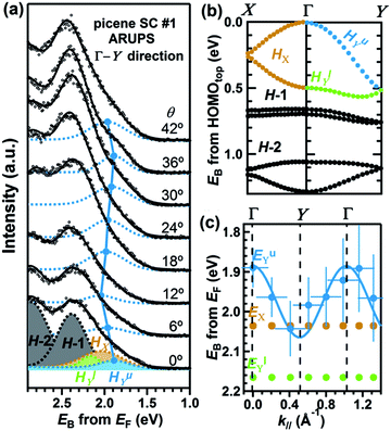 |
| | Fig. 23 (a) ARUPS of the single crystal picene taken along the Γ–Y direction with deconvoluted HX, HuY, HuY, H-1, and H-2 Voigt functions. The HX, HlY, H-1, and H-2, and the shade part of HuY of θ = 6–42° and are omitted for clarity. (b) A part of the calculated valence band structure of picene SC along Γ–Y and Γ–X.172,173 (c) The dispersion of HX, HuY, HlY with respect to the parallel component of electron wave vector. The solid curve is a fit to the 1D-TB model. Reproduced from ref. 115 with permission (Copyright 2012, American Physical Society). | |
(5) Perylene.
Perylene is one of the most traditional benchmark molecule of the organic semiconductors. One of the most essential functionalities of the semiconductors, that is regulation of the electric conductivity via impurity doping, was first achieved in this molecule through the doping of bromine molecules,174 which opened a route to the development of charge-transfer complexes (or frequently cited as organic conductors).15 Undoped perylene is also an interesting research target as an intrinsic semiconductor because it was reported that the electron mobility in zone-refined α-phase single crystals of this molecule exceeded 100 cm2 V−1 s−1 upon cooling the sample temperature below 30 K.175 On the other hand, a band calculation has predicted a moderate total width (∼0.25 eV) of the valence bands of α-perylene,176 and the hole mobility magnitudes at RT have been reported to be in the order of 10−3–10−1 cm2 V−1 s−1.177–181
Photoelectron spectroscopy measurements on the α-perylene single crystal samples have been attempted since relatively early days.109,110,182 Recently, Pookpanratana et al. conducted ARTOF measurements on the α-perylene single crystals to reveal an absence of the E–K dispersion in any in-plane directions.181 Common to the case of tetracene, molecular rearrangement at the surface may be reasons for the absence of the valence band dispersion. They also noted possible thermal disordering of the crystal due to a relatively high vapor pressure of perylene.183 Actually, temperature dependence of the vapor pressure of perylene exhibited very close behavior to that of tetracene,184 and atomic force microscopy observations have revealed that surface roughing of the α-perylene single crystal was induced in vacuum conditions even at RT.185
(6) Organic–inorganic hybrid lead-halide perovskites.
Lead-halide-based organic–inorganic hybrid compounds with the perovskite structures [Fig. 24(a)], hereafter indicated as halide perovskites, are currently attracting tremendous interests as the functional materials of emerging solar cells and high-efficiency light emitting diodes.186–189 Despite an enormous number of publications and rapid evolution of their optoelectronic applications, still many puzzles about their solid-state physical properties are remain unsolved. These compounds are classed as ionic crystals. However, whereas typical ionic crystals are hard and brittle, the halide perovskites are generally soft and even fluctuating.190 This lattice softness makes the “mass” of the charge carriers in these materials heavier than the band effective mass via polaronic effects which are strongly related to electron–phonon coupling.191,192 In this sense, the halide perovskites share common characteristics of the charge carrier transport with the organic semiconductors30,193 even though constitutions of the solid state are distinct from each other.
 |
| | Fig. 24 (a) Schematic drawing of the (cubic) perovskite structure. (b) The bulk (3-D) and surface Brillouin zone of the cubic lattice. | |
Unambiguous one-to-one correlations between structures and electronic properties are desired for resolving such questions of inherent transport natures in the halide perovskite materials, and thus the single crystal samples are most suitable targets for approaching the fundamental properties of these compounds. However, exploration into the electronic band structures of the single crystal halide perovskites by photoemission measurements entails several technical hurdles. For instance, irradiation by high energy photons causes decomposition of the halide perovskite,194,195 which is common to or even severer than the cases of the single crystal organic semiconductors. Another problem which is not the case for the aforementioned organic semiconductors arises when the three-dimensional (3-D) electronic bands are projected on the 2-D SBZ. The ideal (simplest) perovskite structure belongs to the cubic crystal system. The BZ of the cubic lattice is cubic which has four inequivalent symmetry points (Γ, X, M, and R), as illustrated in Fig. 24(b). As described in Section II.11, variation in the emission angle θ does change k⊥ as well as k‖ of photoelectrons; in other words, the ARUPS measurement at a fixed excitation energy surveys a curved surface instead of a plane at a certain k⊥. Accordingly, one has to be cautious enough in making an interpretation about which direction (e.g., Γ–X or X–M for the cubic crystals) in the bulk 3-D BZ is mainly represented in an ARUPS result taken along one in-plane orientation of the SBZ (e.g., ![[capital Gamma, Greek, macron]](https://www.rsc.org/images/entities/i_char_e0ba.gif) –
–![[X with combining macron]](https://www.rsc.org/images/entities/i_char_0058_0304.gif) ). In addition, as mentioned in Section II.10, a limited photoelectron probing depth (i.e., the z position of the electron) leads to an ambiguity in k⊥ (i.e., the surface-parallel momentum of the electron) because of the uncertainty relation. For the cubic crystals, therefore, energy dispersion along a surface parallel direction (e.g. Γ–X) instantaneously means existence of an energetic variances in the equivalent surface normal component, which makes it difficult to determine the energy position of the electronic bands from the ARUPS results due to broadening of the spectral components.
). In addition, as mentioned in Section II.10, a limited photoelectron probing depth (i.e., the z position of the electron) leads to an ambiguity in k⊥ (i.e., the surface-parallel momentum of the electron) because of the uncertainty relation. For the cubic crystals, therefore, energy dispersion along a surface parallel direction (e.g. Γ–X) instantaneously means existence of an energetic variances in the equivalent surface normal component, which makes it difficult to determine the energy position of the electronic bands from the ARUPS results due to broadening of the spectral components.
Despite such difficulties, several research groups have challenged the ARUPS measurements on the single crystal halide perovskites.196–200 We herein digest the cases of the single crystal methylammonium lead triiodide (CH3NH3PbI3; MAPI).†††
Lee et al. reported the ARUPS results on MAPI single crystal samples obtained under various excitation photon energies in a range of 74–200 eV.198 For their experiments, the (bulk) crystallographic structures of the samples were determined by X-ray diffraction, and the sample crystals were cleaved by mechanical breakdown in vacuo to obtain the clean surface for the ARUPS measurements. It is known that MAPI exhibits a structural phase transition from the high temperature cubic phase into the tetragonal lattice at 327.4 K.201 Hence their ARUPS measurements conducted at 200 K should represent the electronic (band) structures of MAPI in the tetragonal phase. Signs implying slight E–K dispersion were revealed by ARUPS and excitation energy dependent data, however, the periodicities of the spectral modulation matched the BZ size of the cubic phase instead of the tetragonal. As a plausible origin for this invisible tetragonal periodicity, the authors suggested that a “gap” induced by the cubic–tetragonal distortion may be overwhelmed by the broadened spectral features because the superperiodic potential was weak. In any case, energy dispersion seen in their ARUPS results was too faint and cannot be reproduced by theoretical E–K dispersion relations for neither cubic nor tetragonal phase.202–204 This may be ascribed to insufficient photoionization cross section of the I5p state, which mainly consists the valence band top region of MAPI,205 for this excitation energy range.206 Another point to be taken into account is quality of the sample surface; since MAPI does not have basal nor pinacoidal cleavage, mechanical breakdown of the crystal does not reproducibly give a plane surface of any specific index. Macroscopic inhomogeneity of the surface presumably obscured details of the electronic band structures.
In contrast, Yang and coworkers succeeded in resolving the E–K‖ dispersion of the valence bands on MAPI single crystal samples by ARUPS under the excitation by He-Iα line (21.218 eV) and synchrotron radiation as well.199 The crystal samples were cut along a specific crystal axis by using a knife blade in atmosphere and were immediately introduced into a ultra-high vacuum system. MCP-LEED observations confirmed that the surface lattice was predominantly the (001) face of the cubic MAPI at 350 K and 300 K, while slight incorporation of the tetragonal phase, which became intense on decreasing the temperature to 250 K, was also detected. Fig. 25(a) shows a series of the ARUPS spectra of the MAPI single crystal taken at 300 K along the –![[M with combining macron]](https://www.rsc.org/images/entities/i_char_004d_0304.gif) direction.‡‡‡ The spectral edge of the valence band shifted depending on the electron emission angle. Actually, the shallowest component among those consisting of the valence band spectra shifted by 0.55 eV toward the Fermi level as moving from to [Fig. 25(b)]. As shown in Fig. 25(c), the ARUPS results mapped on the E–K‖ plane is reproduced by calculated band structures along the Γ–M of the cubic MAPI fairly well. The band effective mass of the holes mh* can be derived to be 0.24(10)m0 by the least-squares fitting of the band top at the point with a parabola, as shown in Fig. 26(a). Decreasing the temperature to 250 K slightly reduced mh* to 0.22(10)m0 [Fig. 26(b)]. On the other hand, while the valence band in the – direction dispersed in the same manner as the case of –, the band top at stayed at a deeper energy in comparison to that at , as shown in Fig. 26(c). This indicates that the ARUPS results around rather than the other points in the SBZ should represent the hole transport natures in MAPI. The mh* value estimated above corresponds to the lower limit of the hole drift mobility μD of 83 cm2 V−1 s−1, which is comparable to the experimental magnitudes of the hole mobility in the MAPI single crystals.207,208 The same group also reported the energy dispersion of 0.2 eV along the surface normal direction on the MAPI single crystal by means of excitation energy dependence of the photoemission spectra.209
direction.‡‡‡ The spectral edge of the valence band shifted depending on the electron emission angle. Actually, the shallowest component among those consisting of the valence band spectra shifted by 0.55 eV toward the Fermi level as moving from to [Fig. 25(b)]. As shown in Fig. 25(c), the ARUPS results mapped on the E–K‖ plane is reproduced by calculated band structures along the Γ–M of the cubic MAPI fairly well. The band effective mass of the holes mh* can be derived to be 0.24(10)m0 by the least-squares fitting of the band top at the point with a parabola, as shown in Fig. 26(a). Decreasing the temperature to 250 K slightly reduced mh* to 0.22(10)m0 [Fig. 26(b)]. On the other hand, while the valence band in the – direction dispersed in the same manner as the case of –, the band top at stayed at a deeper energy in comparison to that at , as shown in Fig. 26(c). This indicates that the ARUPS results around rather than the other points in the SBZ should represent the hole transport natures in MAPI. The mh* value estimated above corresponds to the lower limit of the hole drift mobility μD of 83 cm2 V−1 s−1, which is comparable to the experimental magnitudes of the hole mobility in the MAPI single crystals.207,208 The same group also reported the energy dispersion of 0.2 eV along the surface normal direction on the MAPI single crystal by means of excitation energy dependence of the photoemission spectra.209
 |
| | Fig. 25 Electronic structure of the MAPI single crystals along –. (a) ARUPS spectra measured at 300 K with θ steps of 2.76°. Band dispersion marked as guide to the eye (thick blue curve). (b) Comparison between the spectra at the point and the point in order to clearly show the binding energy change due to the dispersion. (c) The second-derivative E–K‖ dispersion map. All spectra were collected using He-Iα (hν = 21.218 eV). The calculated band dispersion based on the cubic phase of MAPI is given with white dashed lines. (inset of c) Photograph of the MAPI single crystal sample. Reproduced from ref. 199 with permission (Copyright 2018, Wiley-VCH Verlag GmbH & Co. KGaA). | |
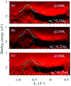 |
| | Fig. 26 The second-derivative E–K‖ dispersion maps near the point at (a) 300 K (the same data as shown in Fig. 25) and (b) 250 K, and (c) near the point at 300 K. The peak positions in the second-derivative spectra are plotted as squares with estimated error bars for the binding energy. The band curvatures close to the point and point are estimated by means of parabolic-curve fitting (given by dashed lines), where the fitting is carried out at the point in the K‖ range of (−0.8 to −0.6) Å−1 and at the point at (−0.7 to −0.4) Å−1, respectively. The corresponding effective mass (mh*) values are indicated. Reproduced from ref. 199 with permission (Copyright 2018, Wiley-VCH Verlag GmbH & Co. KGaA). | |
Afterward, Zu et al. also demonstrated the ARUPS analyses on the single crystal MAPI.200 Their experimental conditions were similar to those of Yang et al.;199 an only apparent difference is that they cleaved the MAPI single crystal surface in a N2-filled glovebox, instead of in air, and the ARUPS measurements were conducted on the samples without air exposure. In this work, the ARUPS results taken along the – and – directions were interpreted to mainly represent the valence band dispersion in the X–M and X–R directions, respectively, as shown in Fig. 27, which was rationalized by a good coincidence of the experimental E–K‖ relationships with band calculation results. The calculation predicts that the VBM of the cubic MAPI is located at the R point of the bulk BZ, which is projected to the point on the SBZ. In fact, the ARUPS results indicated that the spectral edge approaches closest to the Fermi level at . Therefore, it was concluded that the ARUPS results around the point correspond to the E–K‖ dispersion relation at the “global VBM” where the conductive holes are accommodated. The mh* around the point along the – direction was derived to be 0.50(10)m0.
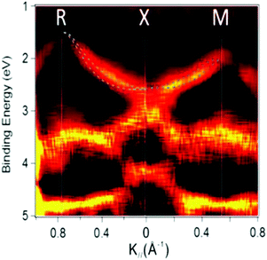 |
| | Fig. 27 The ARUPS intensity map on the E–K‖ plane of the MAPI single crystal along the –– directions. Reproduced from ref. 200 with permission (Copyright 2019, American Chemical Society). | |
This angle-resolved determination of the global VBM enables an unambiguous presumption of the valence band edge energies from BZ-integrated photoelectron energy dispersive curves (EDCs) of polycrystalline MAPI. The analysis of Zu et al. clearly indicated that simple linear extrapolation of the spectral onset—an ordinary way for e.g. organic semiconductor samples—overestimates the binding energy of the band edge of MAPI because of relatively small DOS at the VBM. Instead, they proposed that a semi-logarithmic plot of the EDC—an effective way for disclosing hidden “density of gap states (DOGS)” for organic semiconductors being applicable if very high sensitivity (low background) measurements are available210–213—revealed more reliable information for the band edge position of MAPI.214 While the valence band edge position was determined to be at 1.4 eV below the Fermi level in that work, Yamanaka and coworkers reported an even shallower band edge position (1.2 eV) of the MAPI single crystal clean surface by using low energy (6.5 eV) excitation which extremely highlights the band edge region (Fig. 28).215 Interestingly, their high sensitivity photoemission results also unveiled an existence of the DOGS tailing up to even above the Fermi level for the pristine (uncleaved) surface of the MAPI single crystal. This suggests an occurrence of ground state electron transfer from the surface impurities to the MAPI beneath, in other words, spontaneous hole injection from MAPI to the surface species, which supports efficient hole transfer at the interfaces between hole transporting (donor) molecules and MAPI in practical perovskite solar cell devices.216
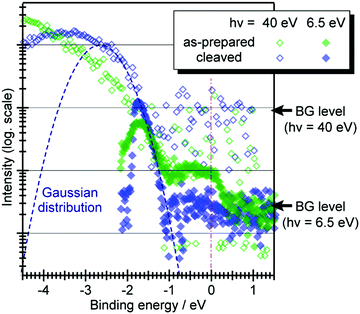 |
| | Fig. 28 Conventional (hν = 40 eV, open symbols) and low energy (hν = 6.5 eV, filled symbols) UPS spectra of the as prepared (green) and cleaved (blue) MAPI single crystal samples plotted in a logarithmic vertical scale. In this graph, the binding energy scale is taken in negative for “bounded” electrons. The intensity scale of the low energy UPS spectra is taken to fulfill smooth inter connection of the valence band onset of the cleaved sample along a Gaussian curve (dashed curve) to represent a merged photoelectron intensity distribution curve for each sample. The original data are taken from ref. 215. | |
2 Other results
(1) High-sensitivity UPS on ultra-purified C60 single crystals.
Since its discovery,217 C60 has long been fascinating researchers in a broad range of scientific circles because of its peculiar characteristics. As an electronic material, this molecule first drew considerable attention by its superconductivity upon alkali metal doping,218,219 and currently it is regarded as a de facto benchmark material for n-type organic semiconductors.220 Uncommonly for the “organic” semiconductors,§§§ this molecule forms an isotropic face-centered-cubic lattice in the solid state at RT owing to its high symmetry character of the molecule itself.37 This—sharing the similar situation to the halide perovskites as discussed above—makes the electronic bands measurements of the C60 crystals quite difficult despite intrinsic electronic structures of this material has been of perpetual interests. Although several works were addressed for clarification of the valence (and conduction) band structures by means of angle-resolved (inverse) photoemission on the single crystals or crystalline films of C60,221–226 these were unlikely to succeed in capturing true figures of the electronic bands, as conclusively reviewed by Gensterblum.227
Even though detailed E–K dispersion relations in the electronic bands and thus the effective masses of charge carriers in C60 have not been attained experimentally, significant features potentially impact the transport characteristics were unveiled by ultralow-background and high-sensitivity UPS210 in the energy gap region of highly-purified (“seven-nine”228) single crystal samples of C60.213Fig. 29 shows the UPS spectra of a C60 single crystal sample (red marks) and a conductive tape (“C-tape”; light gray line) bounding the crystal onto the substrate, which were taken under the excitation by the XeIα line and illumination by the secondary laser light (3.06 eV) and are displayed in semi-logarithmic intensity scales. As the XeIα beam spot was not enough small to fit into the size of the C60 single crystal sample, photoemission signals from the C-tape ought to contribute partly to the spectra for the C60 single crystal. Therefore, the pure contribution of C60 was extracted by subtraction of the spectra from the C-tape multiplied by a rescaling factor α, as shown in Fig. 29 and 30. Surprisingly, the single crystal C60 gave even greater DOGS just above the valence band edge than polycrystalline thin films of C60 deposited in an UHV condition (gray marks in Fig. 30). Since the presence of the DOGS at the vicinity of the valence band edge play a role of trap states for the charge carriers and also can regulate of the Fermi level position,229 this factor presumably dominates the intrinsic transport characteristics of C60. On the other hand, an absence of any additional DOGS signal in the further shallower energy range indicated that the contribution of other potential sources of the gap states, e.g. structural imperfections at the grain boundaries, is negligibly small (<1018 eV−1 cm−3) in the case of C60.
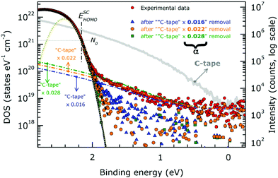 |
| | Fig. 29 XeIα (hν = 8.437 eV) UPS spectrum (log scale intensity plot) of C60 single crystal in the HOMO and gap binding energy region (red filled circles). The XeIα UPS spectrum of the C-tape (gray continuous curve) was rescaled to reproduce the C60 data in the 0–1.7 eV binding energy range. The rescaled C-tape spectra (for different rescaling factor α) are indicated by dash-dotted lines. Continuous lines are the cumulative fitting curve of the C60-HOMO band resulting from convolution of Gaussian functions. For clarity, only the lower-binding-energy Gaussian component was shown (dark yellow short dotted curve). The DOS value at the HOMO edge (ESCHOMO) is N0 = 1.42 × 10²¹ states eV−1 cm−3 (gray horizontal dotted line). The DOS values (right scale) were obtained from UPS data according to the same procedure described in ref. 210 and 211. The molecular packing density of the fcc phase of C60 was used (1.4 × 10²¹ molecules cm−3).230 Reproduced from ref. 213 with permission (Copyright 2015, American Physical Society). | |
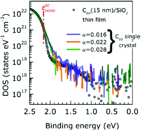 |
| | Fig. 30 Comparison between the DOGS of C60 single crystal (continuous curves, C signal removed; see Fig. 29) and C60 (15 nm)/SiO2 thin film. The data were aligned at the position of the HOMO edge of the C60 single crystal (ESCHOMO, red dash-dotted line). Reproduced from ref. 213 with permission (Copyright 2015, American Physical Society). | |
The physicochemical origin(s) of the DOGS near the valence band edge of the C60 single crystal has not been comprehended yet. Taking into consideration that an emergence of DOGS above the valence band edge was observed upon exposure of the C60 thin films to gaseous atmospheres, and the C60 single crystal samples were persistently exposed to gaseous atmosphere of the ambient pressure until introduction in to the vacuum system since their production, the origin of the DOGS can be ascribed to structural and/or chemical defects induced by penetration of the gas molecules into the C60 lattice. The similar phenomenon of the DOGS formation upon exposure to gaseous atmospheres were also discovered for polycrystalline thin films of pentacene.9,211 It is interesting to note that, however, any sign of the DOGS induced by gas exposure was not observed for pentacene thin films of a larger mean crystallite size suggesting that the existence of grain boundaries are crucial for penetration of the gas molecules into the solid state pentacene, whereas the occurrence of the DOGS was confirmed even on the single crystal samples of extremely fewer grain boundaries for the C60 case. In other words, these findings implied that the C60 crystals are more vulnerable to the penetration of the gas molecules and the emergence of the DOGS in accordance than pentacene. Some unique properties of the solid state C60, for instance the orientational disordering of the individual C60 molecules231,232 and relatively large octahedral voids in the fcc lattice which is known to allow intercalation of various gas molecules,233 are presumed as the origins of this peculiar phenomenon.
(2) High-resolution XPS on the single crystal pentacene.
X-ray photoelectron spectroscopy (XPS) is a useful methodology for “chemical analysis” of specimens.234,235 Whereas this technique is now utilized routinely in the materials chemistry field, its application to organic semiconductor single crystals is obstructed by technical difficulties, namely the sample charging and radiation damage, as described in Section II.12. These problems are common to the cases of the (AR)UPS measurements but are rather severer for the XPS because the high energy excitation inevitably accompanies redundant secondary electron emission and also raises the risks of decomposition and/or polymerization of the sample molecules initiated by high-speed photoelectrons. In addition, limitation in the sizes of the organic semiconductor single crystal samples, which are typically not wider than a few mm2, is generally problematic for conducting reliable chemical analyses by XPS using standard X-ray tubes due to their unfocused footprints.
High-resolution XPS analyses on the single crystal samples of pentacene were successfully achieved under the following countermeasures against these technical problems.89 First, focused X-ray from the synchrotron orbital radiation was adopted to confine the excitation light within the sample areas. Second, in the same way as the case of the ARUPS measurements [see Section III.1.(3)], the samples were illuminated by an assistance laser light (405 nm) to enhance photoconductivity of the pentacene crystals. This was mandatory for getting rid of the sample charging. For the sake of minimizing the X-ray induced radiation damage as well as the sample charging, the excitation photon flux was reduced by interposing a metal (Mg) filter. It is also noteworthy that, paradoxically, undulator beamlines are suited for providing properly weak excitation light because the emittance can be regulated by changing the undulator gap width. In addition, the samples were positively biased at +20 V with respect to the ground for the sake of cutting the total photocurrent below 1 pA. Since the C1s spectral profiles obtained on the pentacene single crystal samples were reasonably accurate (as discussed below) and no energy shift as well as no spectral distortion was observed even after continuous XPS measurements for twelve hours, it can be concluded that these countermeasures were actually effective for suppressing the sample charging and the radiation damage.
Fig. 31 shows C1s XPS spectra of a pentcene single crystal (Pn SC) sample taken under several excitation energies plotted together with a C1s spectrum from the gas phase pentacene¶¶¶ reported by Alagia et al.236 For the gas phase spectra, an asymmetric peak profile with a shoulder in the low binding energy side was attributed to a distribution of chemical shifts for non-equivalent carbon atoms consisting of the pentacene molecule as illustrated in the inset image. The XPS spectra on the Pn SC were as sharp as that for the gas phase pentacene to clearly resolved the two spectral components (“I” and “II”) comprising the C1s main peak. This strongly supported that any spectral distortion due to the sample charging and radiation damage can be ruled out for these results. For that Pn SC sample, a presence of the O1s signal indicated existence of impurities including oxygen atom(s). The number ratio of the oxygen atoms to the carbons was evaluated to be 1.7% based on a quantitative analysis of the peak intensities and reported photoionization cross section for C1s and O1s.206
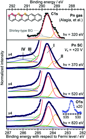 |
| | Fig. 31 C1s XPS spectra of the gas phase (top panel) and single crystal (the other panels) of pentacene depending on the excitation energy. The four components are designated as ‘I’ to ‘IV’. The O1s spectrum taken by the excitation energy of 820 eV is exhibited in a 20 times extended vertical scale to the C1s main feature as an inset graph. The original data in the top panel and the other panels are taken from ref. 89 and 236, respectively. | |
The C1s peak from the Pn SC was accompanied by additional small features (“III” and “IV”) in the high binding energy side. Relative intensities of these two components to the main peak increased for the lower excitation energies as seen in Fig. 31. Since photoelectrons of a lower kinetic energy exhibit a shorter IMFP for this energy range, this excitation energy dependence implied that origins of the components III and IV were located near the surface. Actually, the former and latter features can be attributed to the surface core level shift237,238 and oxidized impurities formed at the surface, respectively. Contrasting to these two features, the relative intensity of the shoulder component (II) became greater in increasing the excitation energy. This behavior is also understandable taking it into consideration that the carbon atoms giving the component II are located at relatively inner part of the pentacene molecule.
In order to access the intrinsic properties of the Pn SC itself, the surface impurities have to be eliminated. It was confirmed that cleavage of the Pn SC surface in UHV successfully cleared the O1s XPS signals to be under the detection limit.167 Exposure of the cleaved Pn SC sample to the ambient atmosphere for one hour resulted in regeneration of the O1s peak to the equivalent relative intensity to that of Pn SC samples without cleavage. Fig. 32 shows the C1s XPS spectra of a cleaved Pn SC sample before and after the ambient exposure. Whereas an impact of the ambient exposure on the main peak was minor, an important change was brought about in the high binding energy side of the main peak by emergence of the oxide impurities. For the Pn SC sample before ambient exposure, a small peak came out at 2.1 eV high binding energy side from the main peak position. The similar feature was previously found by means of electron energy loss spectroscopy and XPS on vacuum deposited thin films of pentacene.239,240 Taking the energy gap width of pentacene (2.2 eV241) into account, this feature can be attributed to the “shake-up satellite” which is originated from an energy loss process of the primary photoelectrons due to the HOMO–LUMO secondary excitation accompanied by the C1s excitation event. On the other hand, for the Pn SC sample after ambient exposure, photoemission signals ascribed to the oxide species were dominant in that energy region and the satellite structures were utterly overwhelmed. Since such core level satellites potentially provide key information about intra-molecular charge re-distribution concomitant with the electron excitation, this result suggested a possibility of high-resolution XPS on the clean surfaces of molecular single crystals for characterizing intrinsic behavior of excitons as well as charge carriers in organic semiconductor materials.
 |
| | Fig. 32 C1s XPS peak profiles of the vacuum-cleaved pentacene single crystal sample (a) before and (b) after exposure to air and ambient light. (insets) Expanded spectra in the vertical scale. The energy scales are common among all the spectra. The original data are taken from ref. 167. | |
(3) Molecular–molecular heteroepitaxy on the single crystal organic semiconductors.
The experimental methodologies for exploring the valence and core levels electronic structures of the organic semiconductor single crystals are now established as described above. This opens the possibilities for accessing the physicochemical properties of molecular–molecular heterointerfaces through established frameworks of the surface science, which potentially leads to fundamental understandings about essential electronic processes driving the organic light emitting diodes and solar cells. For molecular–metal interfaces, in fact, systematic studies on well-defined interfaces built on metal (or semiconductor) single crystal surfaces has so far underpinned advancement of the organic electronic devices.
The first attempt for the photoemission investigation of the molecular–molecular heterointerfaces built on organic single crystal surfaces was conducted for single crystals of rubrene covered with a normal alkane molecule, tetratetracontane (TTC; C44H90), modeling a semiconductor–insulator interfaces in an OFET structure.242 In that work, an excitation energy of 27 eV was chosen, and the photoemission signals from the valence bands of rubrene was drastically suppressed upon coverage of TTC [Fig. 33(a and b)] due to a short IMFP of the photoelectrons. Nevertheless, a peak originating from the valence bands of rubrene was barely resolved, and moreover the peak profile exhibited transformation depending on the electron emission angle θ, as shown in Fig. 33(c), representing the E–K dispersion of the valence bands. Even though the insufficient data quality hindered determination of the accurate energy positions of the valence bands as a function of K‖, a spectrum integrating these angle-resolved spectra exhibited a substantially unchanged energy width of the valence band peak to that of the uncovered rubrene single crystal, suggesting that the valence band dispersion and the hole effective mass of the rubrene single crystal was not significantly affected by the presence of the adjoining hydrocarbon materials.
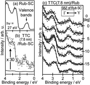 |
| | Fig. 33 UPS spectra of a rubrene single crystal (a) before and (b) after coverage of a 7.8 nm thick TTC overlayer shown with a magnified spectrum. (c) UPS spectra of the 7.8 nm-thick TTC-covered rubrene single crystal obtained at various θ along the Γ–Y direction of the SBZ. For (b) and (c), dots and solid lines represent the raw data and smoothed curves, respectively. (c) is reproduced from ref. 242 with permission (Copyright 2013, Elsevier B.V.). | |
For the TTC-on-rubrene system, while AFM images showing regular arrangements of the TTC overlayers implied molecular ordering at that intermolecular contact, the interface structure was not defined. On the other hand, structural analyses have disclosed well-defined assembly of several organic semiconductor molecules via heteroepitaxial growth on molecular single crystal substrates.243–250 For instance, it was demonstrated by means of surface X-ray diffraction works that n-type semiconductor molecules of C60245 and perfluoropentacene (PFP; C22F14)250 form uniquely oriented crystallites on the single crystal surface of pentacene, and the mean size of these epitaxial crystallites reaches the 100 nm order.246,248 Before closing this article, photoemission analyses conducted on these well-defined molecular–molecular heterointerfaces built on the Pn-SC will be summarized in the following paragraphs.
Yamamoto and co-authors carried out the high-resolution XPS and UPS measurements on the epitaxial heterointerface of C60 on the Pn-SC samples.251 The experimental setup was same as that described in Section III.2.(2). For the sake of deducing the interface electronic structures, evolution of the photoelectron spectra in the core-levels, valence bands, and secondary electron cut-off regions was systematically tracked as shown in Fig. 34. As seen in Fig. 34(a), C1s peaks derived from the donor (pentacene) and acceptor (C60) species can be separated clearly by the high-resolution XPS, which allows ones elucidating the band bending of the both materials toward the interface252 even though each material consists purely of carbon (and hydrogen). In this case, stable energy positions of C1s for both C60 and pentacene represented flat bands of these molecules without any band bending at the interface. Linear increase and decrease of the C1s peak intensities derived from C60 and pentacene [Fig. 34(a)], respectively, indicated that the C60 grows in the Volmer–Weber mode, and the C60 crystallites covers over the Pn-SC surface at the total thickness of ca. 5 nm. This behavior was also confirmed by in situ AFM observation.245 Unchanged energy positions of the highest occupied peak derived from the valence bands of pentacene [Fig. 34(b)] and secondary electron onset [Fig. 34(c)] also represented an absence of strong electronic coupling between C60 and the pentacene molecules in the “head-on” orientation. It is noteworthy that the ultrafast electron transfer across this well-defined molecular heterojunction was demonstrated by time-resolved photoemission electron microscopy in a very recent work,253 which suggests potential advantage of the heteroepitaxial molecular junctions for use of photovoltaic devices with efficient exciton dissociation.
 |
| | Fig. 34 (a) C1s XPS, (b) UPS, and (c) SECO spectra of (o) a pentacene single crystal and that covered with (i) 0.16, (ii) 0.41, (iii) 0.82, (iv) 1.6, (v) 4.1, and (vi) 8.2 nm-thick C60. For the XPS and UPS spectra (except the inset spectrum of b), the Shirley-type background was subtracted. The SECO spectra were normalized by respective maximum intensities. (inset of a) Relative C1s peak intensity of the pentacene (red marks) and C60 (blue) to the total intensity plotted as a function of the C60 thickness. (inset of b) Extended spectra of (v) in a region of the pentacene HOMO. Reproduced from ref. 251 (CC-BY). | |
Uniformity in the crystallographic orientation of the epitaxial molecular heterojunctions enables angle-resolved investigations of the electronic band structures of the overlayer molecules like the successful cases of crystalline molecular thin films on metal single crystal substrates.94–98 Indeed, ARUPS spectra on the epitaxial PFP crystallites grown on the Pn-SC surfaces demonstrated clear variations depending on the electron emission angle representing the E–K dispersion of the valence bands.250 As shown in Fig. 35, the appearance of the ARUPS spectra changed depending on the in-plane sample orientation and reproduced predicted band calculation results254 for corresponding crystallographic axes of the epitaxial PFP crystallites quite reasonably. The energy positions of the valence bands derived from the ARUPS data are plotted as a function of K‖ for three symmetry directions of the SBZ of PFP in Fig. 36. Two spectral components derived by the peak fitting should not be attributed to inequivalent two PFP molecules in the unit cell but to scattered photoelectrons having lost the information of their initial momentum and/or to coexistence of misoriented PFP crystallites. The E–K‖ dispersion relationships of the main valence band component (limed marks) along the three symmetric directions can be reproduced with the 2D-TB approximation (thick curves) fairly well. The intermolecular transfer integral of the highest occupied orbitals between the nearest neighbor PFP molecules (tb) was derived to be −0.093 eV.
 |
| | Fig. 35 ARUPS spectral images of the PFP/Pn-SC sample taken in the Γ–Y (left), Γ–C (middle), and Γ–Z (right) directions plotted on the E–K‖ planes. In these graphs, the binding energy scale is taken in negative. The theoretical band structures254 are plotted as circles. Reproduced from ref. 250 with permission (Copyright 2019, American Chemical Society). | |
 |
| | Fig. 36 Energy positions of the spectral components (upward and downward triangles) of the ARUPS spectra in the (a) Γ–Y, (b) Γ–C, and (c) Γ–Z directions plotted as a function of K‖. 2D-TB fitting results are indicated as thick curves. The inset shows a schematic drawing of the molecular arrangement of the PFP surface unit cell indicating transfer integrals for all four combinations of adjacent molecules. Reproduced from ref. 250 with permission (Copyright 2019, American Chemical Society). | |
Since PFP is regarded as a “complementary” n-type molecule of the p-type pentacene,35 the conduction band structures, rather than the valence bands, are of practical interests. Although the normal photoemission experiments provide information of the occupied electrons directly, large t magnitudes for occupied electronic states generally imply efficient intermolecular coupling also for unoccupied states leading to a notable E–K dispersion of the conduction bands. Actually, the present tb value evaluated from the ARUPS experiments agreed with that derived from the band calculation254 (−0.116 eV) fairly well. This supports an presence of significant intermolecular coupling for the unoccupied molecular orbitals (of ca. +0.07 eV) and E–K dispersion (of ca. 0.3 eV wide) also for the conduction bands of PFP predicted by that calculation. The present result suggests that the conductive electrons in the epitaxial PFP can exhibit the band transport like the holes in the pentacene single crystal beneath; in other words, both electrons and holes have a chance to be delocalized coherently over several molecules at this epitaxial molecular–molecular heterointerface. This indicates great promise of the epitaxially grown organic semiconductor heterojunctions for next generation organic optoelectronic devices by use of efficient transport characteristics in highly-ordered organic semiconductor molecules.255,256
IV. Summary and perspectives
In the present article, we have overviewed attempts and achievements mainly in this decade for exploration into the electronic band dispersion of the single crystals of organic semiconductors and halide perovskites by means of ARUPS. Several essential principles and know-hows of the ARUPS methodology for acquisition of valid data and making reasonable interpretation of the data have also been described with the intention of guiding ones to access one important materials property dominating the charge carrier transport, that is, the effective mass. Furthermore, it has been shown that elaborate analyses of the high-resolution ARUPS data on the single crystals can directly visualize the coupling of the holes with both local vibrations and non-local phonons [Section III.1.(1)] through electron–phonon coupling. As understood from this article, one needs to obtain higher quality ARUPS spectra to elucidate the impact of electron–phonon coupling to the effective mass of quasiparticle, such as effective masses of various polarons. In another side, a new route for accessing the fundamental characters of molecular–molecular contacts through the photoemission experiments on well-defined epitaxial heterojunctions built on molecular single crystal substrates [Section III.2.(3)]. For the future challenging photoemission experiments to look inside of the physical feature of organic semiconductors, we would require their higher-quality single crystals.
Conflicts of interest
There are no conflicts to declare.
Appendix A: meaning and brief explanation of single particle Green's function G0 and G, and relation to the single particle spectral function A(k,E)
Firstly we describe meaning of using the single particle Green's function for the electronic correlation effects. Let's begin with the Green's function for a non-interacting electron system [G0(k,E)], which is defined for Schrödinger equation which has the eigenvalues Ei0(k) with an orthonormal complete system of eigenfunctions φ0i for the unperturbed Hamiltonian H0.| | | (E − H0)G0(k,E) = 1 for H0φ0i = Ei0φ0i → (Ei0 − H0)φ0i = 0 | (A1) |
Then G0(E) is formally written as| | 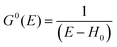 | (A2) |
For concrete computation we write G0(E) by using the completeness of φ0i, eqn (A3), as eqn (A4)| |  | (A3) |
| | 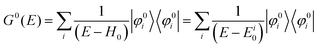 | (A4) |
Then using an infinitesimal δ to overcome the denominator being 0, we write as| | 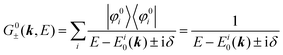 | (A5) |
| |  | (A6) |
where
denotes the principal value.
On the other hand, the density of states, D(E), is defined using δ(x − x0) function as
| | 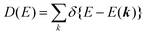 | (A7) |
For the 3-D free electron system (with SC structure of the unit cell length
L),
E–
k relation is
| | 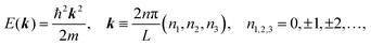 | (A8) |
| | 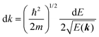 | (A9) |
We change the summation over
k in
eqn (A7) to the integral of
k, then
D(
E) becomes
| | 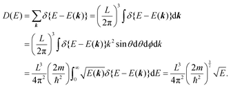 | (A10) |
This is the well-known density of states as a function of
E for a 3-D free electron state, and offers the relation between
G0(
k,
E) and
D(
E) from comparison of
eqn (A2), (A3), (A6), and (A10) as
| | | Im[G0(k,E)] = −πδ{E − E(k)} | (A11) |
| | 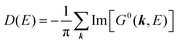 | (A12) |
Furthermore in this case we have following relation for the single electron spectral function of non-interacting system,
A0(
k,
E),
| | 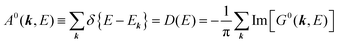 | (A13) |
For the electron interacting system, the single electron spectral function A(k,E), is given by using G(k,E), as in the above non-interacting case. For an electronic system with a perturbation H′, G(k,E) is written as
| | | (E − H)G(E) = 1 for Hφi ≡ (H0 + H′)φi = Eiφi | (A14) |
| | 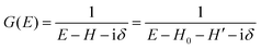 | (A15) |
| | 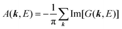 | (A16) |
From comparison of eqn (22) and (27), it is convinced that (i) the spectral peak position is renormalized by Re[Σ(
k,
E)] and peak broadening by Im[Σ(
k,
E)] and (ii) they are related to the density of states described with the imaginary part of Green’s function of the
N-electrons’ system [the right side of eqn (22)].
38,41,44,45,51,52
We can reach formally G(k,E) by the many-body perturbation expansion method starting from the Green's function for a non-interacting N-electrons' system, G0(k,E),38,51,52 as summarized below, where k is an index for the occupied single electron state.
For two operators a and b, if each of which has the inverse operator, there is a following relation,
| | 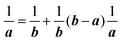 | (A17) |
After putting
a =
G(
E) =
E −
H (where
H =
H0 +
H′) and
b =
G0(
E) =
E −
H0i0, one finds that
G(
E) is expanded using
G0(
E) as,
| | 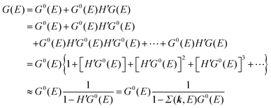 | (A18) |
This relation indicates that
G(
k,
E) is approximately given by using
G0(
k,
E) and therefore we reach
φi and
Ei, as we can easily obtain results for non-interacting system.
Appendix B: matrix elements of effective mass tensors
The crystal lattice can be aligned to the principal axes of the system if angle of these lattice axes, αβγ, are orthogonal. In this case, the origin of its reciprocal lattice is at the band extremum position for many of organic crystals. If the E = E(k) dispersion relation is approximated with a parabolic curve at the extremum point, all off-diagonal terms in the reciprocal effective mass tensor [(1/m*)ij] and the effective mass tensor (mij*) vanish to have only diagonal terms. This means that if we assume parabolic dispersion near the bottom of LUMO and the top of HOMO to define the effective mass of an electron (me*) and a hole (mh*), respectively, the effective masses become scalar. Concrete matrixes of (1/m*)ij and mij* are shown here.
The concrete matrix of the reciprocal effective mass (1/m*) is given as
| | 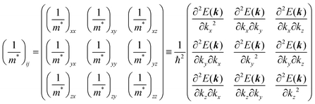 | (B1) |
Then effective mass tensor becomes
| | 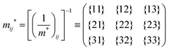 | (B2) |
Each element of the
mij* matrix, {
ij}, is obtained using elements of (1/
m*)
ij given in
eqn (B1) as shown in eqn (B3),
| |  | (B3) |
where concrete elements are given only for {12}, {22}, {32}. As understood from the terms in the each elements, there are various crossing terms such as including
 etc.
etc. If the dispersions are the same along the three main axes, off-diagonal elements disappear. If the off-diagonal elements do not disappear, it is very difficult to obtain accurate effective masses along such off-diagonal related directions. Moreover, we cannot measure
mij* (for
i ≠
j) of the hole (electron) selectively with ARUPS (ARIPES) experiments.
Acknowledgements
NU is very grateful to the late Professor Kazuhiko Seki (Nagoya University) for continuous discussion for 35 years for the challenging research on the electronic band structure of organic molecular crystals and Prof. Masahiro Kotani (Gakushuin University) for his teaching us methods of handling organic semiconductor single crystals. The authors thank Prof. D. Cahen (Weizmann Institute of Science), Prof. A. Kahn (Princeton University), Prof. N. Koch (Humboldt-Universität zu Berlin) and Prof. K. Leo (Technische Universität Dresden) for fruitful discussion on a method of overcoming the scientific gap between electronic structure and charge transport property in organic semiconductor devices. They are very grateful to Prof. H. Ishii (Chiba University), Prof. Y. Kubozono (Okayama University), Prof. H. Aoki (University of Tokyo), Prof. M. Hiramoto (Institute for Molecular Science), and their groups for collaboration on band structure projects of the single crystal. They also appreciate many Post-Doc researchers at Chiba University for realizing and doing risky ARUPS measurements coupled with photoconduction [Prof. S. Duhm (Soochow University), Prof. Q. Xin (Shandong University), Dr F. Bussolotti (Institute of Materials Research and Engineering (IMRE)), and Prof. J.-P. Yang (Yangzhou University)]. We are also grateful to many students of the above laboratories who helped the research. The authors acknowledge financial support, in particular during the last 20 years, by the Global COE Program of MEXT (G03: Advanced School for Organic Electronics), the 21-Century COE Program of MEXT (G-4: Frontiers of Super-Functionality Organic Devices), JSPS KAKENHI (JP26248062, JP24245034, JP20245039, JP20656002, JP23360005, JP20685014, JP13450005, JP17685019, JP14GS0213, JP19002, JP16K14102, JP15H05498, JP23750209, JP18H03904). YN would like to thank TEPCO Memorial Foundation, Yazaki Memorial Foundation for Science and Technology, Izumi Science and Technology Foundation, JGC-S Scholarship Foundation, The Precise Measurement Technology Promotion Foundation, and The Futaba Foundation for their financial supports for this subject.
References
-
S. M. Sze, Physics of Semiconductor Devices, John Wiley & Sons, Inc., New York, 2nd edn, 1981 Search PubMed.
- H. Brooks, Adv. Electron. Electron Phys., 1955, 7, 85–182 CrossRef CAS.
- J. C. Phillips, Phys. Rev., 1962, 125, 1931–1936 CrossRef CAS.
- K. Kudo, M. Yamashina and T. Moriizumi, Jpn. J. Appl. Phys., 1984, 23, 130 CrossRef CAS.
- C. W. Tang, Appl. Phys. Lett., 1986, 48, 183–185 CrossRef CAS.
- C. W. Tang and S. A. VanSlyke, Appl. Phys. Lett., 1987, 51, 913–915 CrossRef CAS.
- M. Hiramoto, H. Fujiwara and M. Yokoyama, Appl. Phys. Lett., 1991, 58, 1062–1064 CrossRef CAS.
- J. J. M. Halls, C. A. Walsh, N. C. Greenham, E. A. Marseglia, R. H. Friend, S. C. Moratti and A. B. Holmes, Nature, 1995, 376, 498–500 CrossRef CAS.
- J.-P. Yang, F. Bussolotti, S. Kera and N. Ueno, J. Phys. D: Appl. Phys., 2017, 50, 423002 CrossRef.
- I. Salzmann, G. Heimel, S. Duhm, M. Oehzelt, P. Pingel, B. M. George, A. Schnegg, K. Lips, R.-P. Blum, A. Vollmer and N. Koch, Phys. Rev. Lett., 2012, 108, 035502 CrossRef PubMed.
- M. Schwarze, W. Tress, B. Beyer, F. Gao, R. Scholz, C. Poelking, K. Ortstein, A. A. Gunther, D. Kasemann, D. Andrienko and K. Leo, Science, 2016, 352, 1446–1449 CrossRef CAS PubMed.
- N. Ueno, Science, 2016, 352, 1395–1396 CrossRef CAS PubMed.
- M. Schwarze, C. Gaul, R. Scholz, F. Bussolotti, A. Hofacker, K. S. Schellhammer, B. Nell, B. D. Naab, Z. Bao, D. Spoltore, K. Vandewal, J. Widmer, S. Kera, N. Ueno, F. Ortmann and K. Leo, Nat. Mater., 2019, 18, 242–248 CrossRef CAS PubMed.
- J.-P. Yang, W.-Q. Wang, F. Bussolotti, L.-W. Cheng, Y.-Q. Li, S. Kera, J.-X. Tang, X.-H. Zeng and N. Ueno, Appl. Phys. Lett., 2016, 109, 093302 CrossRef.
- H. Inokuchi, Org. Electron., 2006, 7, 62–76 CrossRef CAS.
- D. D. Eley, Nature, 1948, 162, 819 CrossRef CAS PubMed.
- A. T. Vartanyan, Zh. Fiz. Khim., 1948, 22, 769–782 CAS.
- N. Karl, Synth. Met., 2003, 133–134, 649–657 CrossRef CAS.
- M. E. Gershenson, V. Podzorov and A. F. Morpurgo, Rev. Mod. Phys., 2006, 78, 973–989 CrossRef CAS.
- T. Hasegawa and J. Takeya, Sci. Technol. Adv. Mater., 2009, 10, 024314 CrossRef PubMed.
- D. Braga and G. Horowitz, Adv. Mater., 2009, 21, 1473–1486 CrossRef CAS.
- C. Wang, H. Dong, L. Jiang and W. Hu, Chem. Soc. Rev., 2018, 47, 422–500 RSC.
- X. Zhang, H. Dong and W. Hu, Adv. Mater., 2018, 30, 1801048 CrossRef PubMed.
- V. Coropceanu, J. Cornil, D. A. da Silva Filho, Y. Olivier, R. Silbey and J.-L. Brédas, Chem. Rev., 2007, 107, 926–952 CrossRef CAS PubMed.
- L. Wang, G. Nan, X. Yang, Q. Peng, Q. Li and Z. Shuai, Chem. Soc. Rev., 2010, 39, 423–434 RSC.
- A. Troisi, Chem. Soc. Rev., 2011, 40, 2347 RSC.
- H. Ishii, N. Kobayashi and K. Hirose, Jpn. J. Appl. Phys., 2019, 58, 110501 CrossRef CAS.
- K. Medjanik, H. Elmers, G. Schönhense, J. Pouget, R. Valenti and M. Lang, Phys. Status Solidi, 2019, 256, 1800745 CrossRef.
- S. Kera, H. Yamane and N. Ueno, Prog. Surf. Sci., 2009, 84, 135–154 CrossRef CAS.
- S. Kera and N. Ueno, J. Electron Spectrosc. Relat. Phenom., 2015, 204, 2–11 CrossRef CAS.
- J. M. Robertson, V. C. Sinclair and J. Trotter, Acta Crystallogr., 1961, 14, 697–704 CrossRef CAS.
- C. Näther, H. Bock, Z. Havlas and T. Hauck, Organometallics, 1998, 17, 4707–4715 CrossRef.
- B. Mahns, O. Kataeva, D. Islamov, S. Hampel, F. Steckel, C. Hess, M. Knupfer, B. Büchner, C. Himcinschi, T. Hahn, R. Renger and J. Kortus, Cryst. Growth Des., 2014, 14, 1338–1346 CrossRef CAS.
- C. C. Mattheus, A. B. Dros, J. Baas, G. T. Oostergetel, A. Meetsma, J. L. de Boer and T. T. M. Palstra, Synth. Met., 2003, 138, 475–481 CrossRef CAS.
- Y. Sakamoto, T. Suzuki, M. Kobayashi, Y. Gao, Y. Fukai, Y. Inoue, F. Sato and S. Tokito, J. Am. Chem. Soc., 2004, 126, 8138–8140 CrossRef CAS PubMed.
- O. D. Jurchescu, A. Meetsma and T. T. M. Palstra, Acta Crystallogr., Sect. B: Struct. Sci., 2006, 62, 330–334 CrossRef PubMed.
- D. L. Dorset and M. P. McCourt, Acta Crystallogr., Sect. A: Found. Crystallogr., 1994, 50, 344–351 CrossRef.
-
G. D. Mahan, Many-Particle Physics, Springer US, Boston, MA, 2000 Search PubMed.
- T. Fujikawa and H. Arai, J. Electron Spectrosc. Relat. Phenom., 2005, 149, 61–86 CrossRef CAS.
- T. Fujikawa, J. Electron Spectrosc. Relat. Phenom., 2009, 173, 51–78 CrossRef CAS.
- S. Moser, J. Electron Spectrosc. Relat. Phenom., 2017, 214, 29–52 CrossRef CAS.
- H. Y. Fan, Phys. Rev., 1945, 68, 43–52 CrossRef CAS.
- C. N. Berglund and W. E. Spicer, Phys. Rev., 1964, 136, A1030–A1044 CrossRef.
-
S. Hüfner, Photoelectron Spectroscopy, Springer Berlin Heidelberg, Berlin, Heidelberg, 3rd edn, 2003 Search PubMed.
- A. Damascelli, Z. Hussain and Z.-X. Shen, Rev. Mod. Phys., 2003, 75, 473–541 CrossRef CAS.
-
E. Heilbronner and H. Bock, Das HMO-Modell und seine Anwendung, Verlag Chemie, Weinheim, Germany, 1970 Search PubMed.
-
P. A. Cox, The electronic structure and chemistry of solids, Oxford University Press, 1st edn, 1987 Search PubMed.
- K. Seki, N. Ueno, U. O. Karlsson, R. Engelhardt and E.-E. Koch, Chem. Phys., 1986, 105, 247–265 CrossRef CAS.
- P. J. Feibelman and D. E. Eastman, Phys. Rev. B: Solid State, 1974, 10, 4932–4947 CrossRef CAS.
-
J. B. Pendley, Low Energy Electron Diffraction: The Theory and Its Application to Determination of Surface Structure, Academic Press Inc., 1974 Search PubMed.
-
R. D. Mattuck, A Guide to Feynman Diagrams in the Many-Body Problem, McGraw-Hill, New York, 1967 Search PubMed.
-
H. Bruus and K. Flensberg, Many-body quantum theory in condensed matter physics: an introduction, Oxford University Press, Oxford, Corrected., 2006 Search PubMed.
- V. Coropceanu, M. Malagoli, D. A. da Silva Filho, N. E. Gruhn, T. G. Bill and J. L. Brédas, Phys. Rev. Lett., 2002, 89, 275503 CrossRef CAS PubMed.
- H. Yamane, S. Nagamatsu, H. Fukagawa, S. Kera, R. Friedlein, K. K. Okudaira and N. Ueno, Phys. Rev. B: Condens. Matter Mater. Phys., 2005, 72, 153412 CrossRef.
- H. Fukagawa, H. Yamane, T. Kataoka, S. Kera, M. Nakamura, K. Kudo and N. Ueno, Phys. Rev. B: Condens. Matter Mater. Phys., 2006, 73, 245310 CrossRef.
- G. A. Sawatzky, Nature, 1989, 342, 480–481 CrossRef.
- S. Ciuchi and S. Fratini, Phys. Rev. Lett., 2011, 106, 166403 CrossRef CAS PubMed.
- T. Koopmans, Physica, 1934, 1, 104–113 CrossRef.
- S. Kümmel and L. Kronik, Rev. Mod. Phys., 2008, 80, 3–60 CrossRef.
- T. Permien, R. Engelhardt, C. A. Feldmann and E. E. Koch, Chem. Phys. Lett., 1983, 98, 527–530 CrossRef CAS.
- N. V. Richardson, Chem. Phys. Lett., 1983, 102, 390–391 CrossRef CAS.
- W. D. Grobman, Phys. Rev. B: Solid State, 1978, 17, 4573–4585 CrossRef CAS.
- S. Hasegawa, S. Tanaka, Y. Yamashita, H. Inokuchi, H. Fujimoto, K. Kamiya, K. Seki and N. Ueno, Phys. Rev. B: Condens. Matter Mater. Phys., 1993, 48, 2596–2600 CrossRef CAS PubMed.
- N. Ueno, K. Suzuki, S. Hasegawa, K. Kamiya, K. Seki and H. Inokuchi, J. Chem. Phys., 1993, 99, 7169–7174 CrossRef CAS.
- D. Yoshimura, H. Ishii, Y. Ouchi, E. Ito, T. Miyamae, S. Hasegawa, K. K. Okudaira, N. Ueno and K. Seki, Phys. Rev. B: Condens. Matter Mater. Phys., 1999, 60, 9046–9060 CrossRef CAS.
- S. Kera, S. Tanaka, H. Yamane, D. Yoshimura, K. K. Okudaira, K. Seki and N. Ueno, Chem. Phys., 2006, 325, 113–120 CrossRef CAS.
- N. Ueno, A. Kitamura, K. K. Okudaira, T. Miyamae, Y. Harada, S. Hasegawa, H. Ishii, H. Inokuchi, T. Fujikawa, T. Miyazaki and K. Seki, J. Chem. Phys., 1997, 107, 2079–2088 CrossRef CAS.
- P. Puschnig, S. Berkebile, A. J. Fleming, G. Koller, K. Emtsev, T. Seyller, J. D. Riley, C. Ambrosch-Draxl, F. P. Netzer and M. G. Ramsey, Science, 2009, 326, 702–706 CrossRef CAS PubMed.
- D. Luftner, T. Ules, E. M. Reinisch, G. Koller, S. Soubatch, F. S. Tautz, M. G. Ramsey and P. Puschnig, Proc. Natl. Acad. Sci. U. S. A., 2014, 111, 605–610 CrossRef PubMed.
- M. Wießner, D. Hauschild, C. Sauer, V. Feyer, A. Schöll and F. Reinert, Nat. Commun., 2014, 5, 4156 CrossRef PubMed.
- Y. Li, X. Zhu, P. Lan, Q. Zhang, M. Qin and P. Lu, Phys. Rev. A: At., Mol., Opt. Phys., 2014, 89, 045401 CrossRef.
- F. Bussolotti, J. Yang, T. Yamaguchi, K. Yonezawa, K. Sato, M. Matsunami, K. Tanaka, Y. Nakayama, H. Ishii, N. Ueno and S. Kera, Nat. Commun., 2017, 8, 173 CrossRef CAS PubMed.
-
N. W. Ashcroft and N. D. Mermin, Solid state physics, Holt, Rinehart and Winston, New York, 1976 Search PubMed.
-
L. I. Schiff, Quantum Mechanics, McGraw-Hill, New York, 3rd edn, 1968 Search PubMed.
- A. Troisi and G. Orlandi, J. Phys. Chem. B, 2005, 109, 1849–1856 CrossRef CAS PubMed.
- N. Ueno, K. Seki, N. Sato, H. Fujimoto, T. Kuramochi, K. Sugita and H. Inokuchi, Phys. Rev. B: Condens. Matter Mater. Phys., 1990, 41, 1176–1183 CrossRef CAS PubMed.
- N. Ueno, K. Seki, N. Sato, H. Fujimoto, T. Kuramochi, K. Sugita and H. Inokuchi, Phys. Rev. B: Condens. Matter Mater. Phys., 1990, 42, 3194 CrossRef CAS PubMed.
- N. Ueno and S. Kera, Prog. Surf. Sci., 2008, 83, 490–557 CrossRef CAS.
- P. D. Loly and J. B. Pendry, J. Phys. C: Solid State Phys., 1983, 16, 423–431 CrossRef CAS.
- V. N. Strocov, J. Electron Spectrosc. Relat. Phenom., 2003, 130, 65–78 CrossRef CAS.
- J. Erhart, S. Sponar, G. Sulyok, G. Badurek, M. Ozawa and Y. Hasegawa, Nat. Phys., 2012, 8, 185–189 Search PubMed.
- M. P. Seah and W. A. Dench, Surf. Interface Anal., 1979, 1, 2–11 CrossRef CAS.
- W. P. Davey, Phys. Rev., 1925, 25, 753–761 CrossRef CAS.
-
R. W. G. Wyckoff, Crystal Structures, Interscience Publishers, New York, 2nd edn, 1963, vol. 1 Search PubMed.
- T. Graber, F. Forster, A. Schöll and F. Reinert, Surf. Sci., 2011, 605, 878–882 CrossRef CAS.
- Y. Ozawa, Y. Nakayama, S. Machida, H. Kinjo and H. Ishii, J. Electron Spectrosc. Relat. Phenom., 2014, 197, 17–21 CrossRef CAS.
- P. Thiry, D. Chandesris, J. Lecante, C. Guillot, R. Pinchaux and Y. Pétroff, Phys. Rev. Lett., 1979, 43, 82–85 CrossRef CAS.
- F. J. Himpsel, Appl. Opt., 1980, 19, 3964 CrossRef CAS PubMed.
- Y. Nakayama, Y. Uragami, M. Yamamoto, K. Yonezawa, K. Mase, S. Kera, H. Ishii and N. Ueno, J. Phys.: Condens. Matter, 2016, 28, 094001 CrossRef PubMed.
- B. Boudaïffa, P. Cloutier, D. Hunting, M. A. Huels and L. Sanche, Science, 2000, 287, 1658–1660 CrossRef PubMed.
- H. Yoshida, Rev. Sci. Instrum., 2013, 84, 103901 CrossRef PubMed.
- S. Hasegawa, T. Mori, K. Imaeda, S. Tanaka, Y. Yamashita, H. Inokuchi, H. Fujimoto, K. Seki and N. Ueno, J. Chem. Phys., 1994, 100, 6969–6973 CrossRef CAS.
- N. Koch, A. Vollmer, I. Salzmann, B. Nickel, H. Weiss and J. P. Rabe, Phys. Rev. Lett., 2006, 96, 156803 CrossRef CAS PubMed.
- H. Kakuta, T. Hirahara, I. Matsuda, T. Nagao, S. Hasegawa, N. Ueno and K. Sakamoto, Phys. Rev. Lett., 2007, 98, 247601 CrossRef PubMed.
- E. Annese, C. E. Viol, B. Zhou, J. Fujii, I. Vobornik, C. Baldacchini, M. G. Betti and G. Rossi, Surf. Sci., 2007, 601, 4242–4245 CrossRef CAS.
- H. Yamane, D. Yoshimura, E. Kawabe, R. Sumii, K. Kanai, Y. Ouchi, N. Ueno and K. Seki, Phys. Rev. B: Condens. Matter Mater. Phys., 2007, 76, 165436 CrossRef.
- R. C. Hatch, D. L. Huber and H. Höchst, Phys. Rev. B: Condens. Matter Mater. Phys., 2009, 80, 081411 CrossRef.
- M. Ohtomo, T. Suzuki, T. Shimada and T. Hasegawa, Appl. Phys. Lett., 2009, 95, 123308 CrossRef.
- L. Jiang, H. Dong, Q. Meng, H. Li, M. He, Z. Wei, Y. He and W. Hu, Adv. Mater., 2011, 23, 2059–2063 CrossRef CAS PubMed.
- J. Soeda, T. Uemura, T. Okamoto, C. Mitsui, M. Yamagishi and J. Takeya, Appl. Phys. Express, 2013, 6, 076503 CrossRef.
- D. He, Y. Zhang, Q. Wu, R. Xu, H. Nan, J. Liu, J. Yao, Z. Wang, S. Yuan, Y. Li, Y. Shi, J. Wang, Z. Ni, L. He, F. Miao, F. Song, H. Xu, K. Watanabe, T. Taniguchi, J.-B. Xu and X. Wang, Nat. Commun., 2014, 5, 5162 CrossRef CAS PubMed.
- A. Yamamura, S. Watanabe, M. Uno, M. Mitani, C. Mitsui, J. Tsurumi, N. Isahaya, Y. Kanaoka, T. Okamoto and J. Takeya, Sci. Adv., 2018, 4, eaao5758 CrossRef PubMed.
- Y. Shi, L. Jiang, J. Liu, Z. Tu, Y. Hu, Q. Wu, Y. Yi, E. Gann, C. R. McNeill, H. Li, W. Hu, D. Zhu and H. Sirringhaus, Nat. Commun., 2018, 9, 2933 CrossRef PubMed.
- L. Jiang, J. Liu, Y. Shi, D. Zhu, H. Zhang, Y. Hu, J. Yu, W. Hu and L. Jiang, J. Mater. Chem. C, 2019, 7, 3436–3442 RSC.
- J. Liu, L. Jiang, W. Hu, Y. Liu and D. Zhu, Sci. China: Chem., 2019, 62, 313–330 CrossRef CAS.
- M. Kikuchi, K. Takagi, H. Naito and M. Hiramoto, Org. Electron., 2017, 41, 118–121 CrossRef CAS.
- D. A. Huchital and R. T. McKeon, Appl. Phys. Lett., 1972, 20, 158–159 CrossRef CAS.
- J. Cazaux, J. Electron Spectrosc. Relat. Phenom., 2000, 113, 15–33 CrossRef CAS.
- U. Zimmermann, G. Schnitzler, V. Wüstenhagen, N. Karl, R. Dudde, E. E. Koch and E. Umbach, Mol. Cryst. Liq. Cryst. Sci. Technol., Sect. A, 2000, 339, 231–259 CrossRef CAS.
- B. M. Schmid, N. Sato and H. Inokuchi, Chem. Lett., 1983, 1897–1900 CrossRef CAS.
- N. Sato, H. Inokuchi, B. M. Schmid and N. Karl, J. Chem. Phys., 1985, 83, 5413–5419 CrossRef CAS.
- A. Vollmer, O. D. Jurchescu, I. Arfaoui, I. Salzmann, T. T. M. Palstra, P. Rudolf, J. Niemax, J. Pflaum, J. P. Rabe and N. Koch, Eur. Phys. J. E: Soft Matter Biol. Phys., 2005, 17, 339–343 CrossRef CAS PubMed.
- S. Machida, Y. Nakayama, S. Duhm, Q. Xin, A. Funakoshi, N. Ogawa, S. Kera, N. Ueno and H. Ishii, Phys. Rev. Lett., 2010, 104, 156401 CrossRef PubMed.
- N. Sai, M. L. Tiago, J. R. Chelikowsky and F. A. Reboredo, Phys. Rev. B: Condens. Matter Mater. Phys., 2008, 77, 161306 CrossRef.
- Q. Xin, S. Duhm, F. Bussolotti, K. Akaike, Y. Kubozono, H. Aoki, T. Kosugi, S. Kera and N. Ueno, Phys. Rev. Lett., 2012, 108, 226401 CrossRef PubMed.
- W. Xie, P. L. Prabhumirashi, Y. Nakayama, K. A. McGarry, M. L. Geier, Y. Uragami, K. Mase, C. J. Douglas, H. Ishii, M. C. Hersam and C. D. Frisbie, ACS Nano, 2013, 7, 10245–10256 CrossRef CAS PubMed.
- Y. Nakayama, Y. Mizuno, M. Hikasa, M. Yamamoto, M. Matsunami, S. Ideta, K. Tanaka, H. Ishii and N. Ueno, J. Phys. Chem. Lett., 2017, 8, 1259–1264 CrossRef CAS PubMed.
-
C. Kloc, T. Siegrist and J. Pflaum, Springer Handbook of Crystal Growth, Springer Berlin Heidelberg, Berlin, Heidelberg, 2010, pp. 845–867 Search PubMed.
- S. Z. Bisri, T. Takenobu, T. Takahashi and Y. Iwasa, Appl. Phys. Lett., 2010, 96, 183304 CrossRef.
- Y. Nakayama, M. Iwashita, M. Kikuchi, R. Tsuruta, K. Yoshida, Y. Gunjo, Y. Yabara, T. Hosokai, T. Koganezawa, S. Izawa and M. Hiramoto, Materials, 2020, 13, 1978, DOI:10.3390/ma13081978.
- V. C. Sundar, J. Zaumseil, V. Podzorov, E. Menard, R. L. Willett, T. Someya, M. E. Gershenson and J. A. Rogers, Science, 2004, 303, 1644–1646 CrossRef CAS PubMed.
- V. Podzorov, E. Menard, A. Borissov, V. Kiryukhin, J. A. Rogers and M. E. Gershenson, Phys. Rev. Lett., 2004, 93, 086602 CrossRef CAS PubMed.
- V. Podzorov, E. Menard, J. A. Rogers and M. E. Gershenson, Phys. Rev. Lett., 2005, 95, 226601 CrossRef CAS.
- J. Takeya, K. Tsukagoshi, Y. Aoyagi, T. Takenobu and Y. Iwasa, Jpn. J. Appl. Phys., 2005, 44, L1393–L1396 CrossRef CAS.
- J. Takeya, M. Yamagishi, Y. Tominari, R. Hirahara, Y. Nakazawa, T. Nishikawa, T. Kawase, T. Shimoda and S. Ogawa, Appl. Phys. Lett., 2007, 90, 102120 CrossRef.
- D. A. da Silva Filho, E.-G. Kim and J.-L. Brédas, Adv. Mater., 2005, 17, 1072–1076 CrossRef CAS.
- Z. Q. Li, V. Podzorov, N. Sai, M. C. Martin, M. E. Gershenson, M. Di Ventra and D. N. Basov, Phys. Rev. Lett., 2007, 99, 016403 CrossRef CAS PubMed.
- Y. Nakayama, S. Machida, T. Minari, K. Tsukagishi, Y. Noguchi and H. Ishii, Appl. Phys. Lett., 2008, 93, 173305 CrossRef.
- Y. Nakayama, S. Machida, D. Tsunami, Y. Kimura, M. Niwano, Y. Noguchi and H. Ishii, Appl. Phys. Lett., 2008, 92, 153306 CrossRef.
- Y. Nakayama, Y. Uragami, S. Machida, K. R. Koswattage, D. Yoshimura, H. Setoyama, T. Okajima, K. Mase and H. Ishii, Appl. Phys. Express, 2012, 5, 111601 CrossRef.
- H. Ding, C. Reese, A. J. Mäkinen, Z. Bao and Y. Gao, Appl. Phys. Lett., 2010, 96, 222106 CrossRef.
- J. Nitta, K. Miwa, N. Komiya, E. Annese, J. Fujii, S. Ono and K. Sakamoto, Sci. Rep., 2019, 9, 9645 CrossRef PubMed.
- A. Vollmer, R. Ovsyannikov, M. Gorgoi, S. Krause, M. Oehzelt, A. Lindblad, N. Mårtensson, S. Svensson, P. Karlsson, M. Lundvuist, T. Schmeiler, J. Pflaum and N. Koch, J. Electron Spectrosc. Relat. Phenom., 2012, 185, 55–60 CrossRef CAS.
- S. Yanagisawa, Y. Morikawa and A. Schindlmayr, Phys. Rev. B: Condens. Matter Mater. Phys., 2013, 88, 115438 CrossRef.
- S. Duhm, Q. Xin, S. Hosoumi, H. Fukagawa, K. Sato, N. Ueno and S. Kera, Adv. Mater., 2012, 24, 901–905 CrossRef CAS PubMed.
- A. Girlando, L. Grisanti, M. Masino, I. Bilotti, A. Brillante, R. G. Della Valle and E. Venuti, Phys. Rev. B: Condens. Matter Mater. Phys., 2010, 82, 035208 CrossRef.
- A. Bree and L. E. Lyons, J. Chem. Phys., 1954, 22, 1630 CrossRef CAS.
- L. E. Lyons, J. Chem. Phys., 1955, 23, 220 CrossRef CAS.
- E. L. Frankevich and E. I. Balabanov, Phys. Status Solidi, 1966, 14, 523–529 CrossRef CAS.
- A. Szymanski and M. M. Labes, J. Chem. Phys., 1969, 50, 1898–1899 CrossRef CAS.
- A. K. Ghosh and T. Feng, J. Appl. Phys., 1973, 44, 2781–2788 CrossRef CAS.
- M. B. Smith and J. Michl, Chem. Rev., 2010, 110, 6891–6936 CrossRef CAS PubMed.
- J. Lee, P. Jadhav, P. D. Reusswig, S. R. Yost, N. J. Thompson, D. N. Congreve, E. Hontz, T. Van Voorhis and M. A. Baldo, Acc. Chem. Res., 2013, 46, 1300–1311 CrossRef CAS PubMed.
- L. E. Lyons and G. C. Morris, J. Chem. Soc., 1960, 5192 RSC.
- F. I. Vilesov, A. A. Zagrubskii and D. Z. Garbuzov, Sov. Phys. Solid State, 1964, 5, 1460–1464 Search PubMed.
- T. Hirooka, K. Tanaka, K. Kuchitsu, M. Fujihira, H. Inokuchi and Y. Harada, Chem. Phys. Lett., 1973, 18, 390–393 CrossRef CAS.
- K. Seki, Y. Harada, K. Ohno and H. Inokuchi, Bull. Chem. Soc. Jpn., 1974, 47, 1608–1610 CrossRef CAS.
- N. Ueno, Y. Hayasi and S. Kiyono, Chem. Phys. Lett., 1975, 35, 31–34 CrossRef CAS.
- M. Pope, J. Burgos and J. Giachino, J. Chem. Phys., 1965, 43, 3367–3371 CrossRef CAS.
- S. Arnold, M. Pope and T. K. T. Hsieh, Phys. Status Solidi, 1979, 94, 263–272 CrossRef CAS.
- R. Katoh and M. Kotani, Chem. Phys. Lett., 1992, 196, 103–107 CrossRef CAS.
- C. Goldmann, S. Haas, C. Krellner, K. P. Pernstich, D. J. Gundlach and B. Batlogg, J. Appl. Phys., 2004, 96, 2080–2086 CrossRef CAS.
- C. Reese, W.-J. Chung, M. Ling, M. Roberts and Z. Bao, Appl. Phys. Lett., 2006, 89, 202108 CrossRef.
- Y. C. Cheng, R. J. Silbey, D. A. da Silva Filho, J. P. Calbert, J. Cornil and J. L. Brédas, J. Chem. Phys., 2003, 118, 3764–3774 CrossRef CAS.
- K. Hummer and C. Ambrosch-Draxl, Phys. Rev. B: Condens. Matter Mater. Phys., 2005, 72, 205205 CrossRef.
- M. Ohtomo, K. Itaka, T. Hasegawa and T. Shimada, Appl. Phys. Express, 2011, 4, 021601 CrossRef.
- H. Morisaki, T. Koretsune, C. Hotta, J. Takeya, T. Kimura and Y. Wakabayashi, Nat. Commun., 2014, 5, 5400 CrossRef CAS PubMed.
- Y.-Y. Lin, D. J. Gundlach, S. F. Nelson and T. N. Jackson, IEEE Electron Device Lett., 1997, 18, 606–608 CAS.
- O. D. Jurchescu, J. Baas and T. T. M. Palstra, Appl. Phys. Lett., 2004, 84, 3061–3063 CrossRef CAS.
- R. C. Haddon, X. Chi, M. E. Itkis, J. E. Anthony, D. L. Eaton, T. Siegrist, C. C. Mattheus and T. T. M. Palstra, J. Phys. Chem. B, 2002, 106, 8288–8292 CrossRef CAS.
- Y. C. Cheng, R. J. Silbey, D. A. da Silva Filho, J. P. Calbert, J. Cornil and J. L. Brédas, J. Chem. Phys., 2003, 118, 3764–3774 CrossRef CAS.
- H. Yoshida and N. Sato, Phys. Rev. B: Condens. Matter Mater. Phys., 2008, 77, 235205 CrossRef.
- Y. Nakayama, Y. Uragami, M. Yamamoto, S. Machida, H. Kinjo, K. Mase, K. R. Koswattage and H. Ishii, Jpn. J. Appl. Phys., 2014, 53, 01AD03 CrossRef.
- Y. Takeyama, S. Ono and Y. Matsumoto, Appl. Phys. Lett., 2012, 101, 083303 CrossRef.
- J. Dong, P. Yu, S. A. Arabi, J. Wang, J. He and C. Jiang, Nanotechnology, 2016, 27, 275202 CrossRef PubMed.
- T. Uemura, M. Yamagishi, J. Soeda, Y. Takatsuki, Y. Okada, Y. Nakazawa and J. Takeya, Phys. Rev. B: Condens. Matter Mater. Phys., 2012, 85, 035313 CrossRef.
- Y. Mizuno, M. Yamamoto, H. Kinjo, K. Mase, H. Ishii, K. K. Okudaira, H. Yoshida and Y. Nakayama, Mol. Cryst. Liq. Cryst., 2017, 648, 216–222 CrossRef CAS.
- Y. Nakayama, M. Hikasa, N. Moriya, M. Meissner, T. Yamaguchi, K. Yoshida, M. Murata, K. Mase, T. Ueba and S. Kera, J. Mater. Res., 2018, 33, 3362–3370 CrossRef CAS.
- J. Y. Lee, S. Roth and Y. W. Park, Appl. Phys. Lett., 2006, 88, 252106 CrossRef.
- Y. Wakabayashi, J. Takeya and T. Kimura, Phys. Rev. Lett., 2010, 104, 066103 CrossRef PubMed.
- R. Mitsuhashi, Y. Suzuki, Y. Yamanari, H. Mitamura, T. Kambe, N. Ikeda, H. Okamoto, A. Fujiwara, M. Yamaji, N. Kawasaki, Y. Maniwa and Y. Kubozono, Nature, 2010, 464, 76–79 CrossRef CAS PubMed.
- T. Kosugi, T. Miyake, S. Ishibashi, R. Arita and H. Aoki, J. Phys. Soc. Jpn., 2009, 78, 113704 CrossRef.
- G. Giovannetti and M. Capone, Phys. Rev. B: Condens. Matter Mater. Phys., 2011, 83, 134508 CrossRef.
- H. Akamatu, H. Inokuchi and Y. Matsunaga, Nature, 1954, 173, 168–169 CrossRef.
- W. Warta, R. Stehle and N. Karl, Appl. Phys. A: Solids Surf., 1985, 36, 163–170 CrossRef.
- I. A. Fedorov, Y. N. Zhuravlev and V. P. Berveno, J. Chem. Phys., 2013, 138, 094509 CrossRef CAS PubMed.
- Y. Maruyama, T. Kobayashi, H. Inokuchi and S. Iwashima, Mol. Cryst. Liq. Cryst., 1973, 20, 373–380 CrossRef CAS.
- M. Kotani, K. Kakinuma, M. Yoshimura, K. Ishii, S. Yamazaki, T. Kobori, H. Okuyama, H. Kobayashi and H. Tada, Chem. Phys., 2006, 325, 160–169 CrossRef CAS.
- J.-W. Lee, H.-S. Kang, M.-K. Kim, K. Kim, M.-Y. Cho, Y.-W. Kwon, J. Joo, J.-I. Kim and C.-S. Hong, J. Appl. Phys., 2007, 102, 124104 CrossRef.
- J. Kougo and K. Ishikawa, Jpn. J. Appl. Phys., 2016, 55, 030304 CrossRef.
- S. J. Pookpanratana, K. P. Goetz, E. G. Bittle, H. Haneef, L. You, C. A. Hacker, S. W. Robey, O. D. Jurchescu, R. Ovsyannikov and E. Giangrisostomi, Org. Electron., 2018, 61, 157–163 CrossRef CAS PubMed.
- N. Karl and N. Sato, Mol. Cryst. Liq. Cryst. Sci. Technol., Sect. A, 1992, 218, 79–84 CrossRef CAS.
- K. Nass, D. Lenoir and A. Kettrup, Angew. Chem., Int. Ed. Engl., 1995, 34, 1735–1736 CrossRef CAS.
- V. Oja and E. M. Suuberg, J. Chem. Eng. Data, 1998, 43, 486–492 CrossRef CAS.
-
Y. Yamada, private communication.
- A. Kojima, K. Teshima, Y. Shirai and T. Miyasaka, J. Am. Chem. Soc., 2009, 131, 6050–6051 CrossRef CAS PubMed.
- Best Research-Cell Efficiency Chart, https://www.nrel.gov/pv/assets/pdfs/best-research-cell-efficiencies.20191106.pdf, accessed 16 January 2020.
- M. A. Green, A. Ho-Baillie and H. J. Snaith, Nat. Photonics, 2014, 8, 506–514 CrossRef CAS.
- S. D. Stranks and H. J. Snaith, Nat. Nanotechnol., 2015, 10, 391–402 CrossRef CAS PubMed.
- C. Katan, A. D. Mohite and J. Even, Nat. Mater., 2018, 17, 377–379 CrossRef CAS PubMed.
- J. M. Frost, Phys. Rev. B, 2017, 96, 195202 CrossRef.
- K. Miyata, T. L. Atallah and X.-Y. Zhu, Sci. Adv., 2017, 3, e1701469 CrossRef PubMed.
- H. Sirringhaus, T. Sakanoue and J.-F. Chang, Phys. Status Solidi, 2012, 249, 1655–1676 CrossRef CAS.
- Y. Li, X. Xu, C. Wang, B. Ecker, J. Yang, J. Huang and Y. Gao, J. Phys. Chem. C, 2017, 121, 3904–3910 CrossRef CAS.
- K. Motoki, Y. Miyazawa, D. Kobayashi, M. Ikegami, T. Miyasaka, T. Yamamoto and K. Hirose, J. Appl. Phys., 2017, 121, 085501 CrossRef.
- D. Niesner, M. Wilhelm, I. Levchuk, A. Osvet, S. Shrestha, M. Batentschuk, C. Brabec and T. Fauster, Phys. Rev. Lett., 2016, 117, 126401 CrossRef PubMed.
- T. Komesu, X. Huang, T. R. Paudel, Y. B. Losovyj, X. Zhang, E. F. Schwier, Y. Kojima, M. Zheng, H. Iwasawa, K. Shimada, M. I. Saidaminov, D. Shi, A. L. Abdelhady, O. M. Bakr, S. Dong, E. Y. Tsymbal and P. A. Dowben, J. Phys. Chem. C, 2016, 120, 21710–21715 CrossRef CAS.
- M.-I. Lee, A. Barragán, M. N. Nair, V. L. R. Jacques, D. Le Bolloc’h, P. Fertey, K. Jemli, F. Lédée, G. Trippé-Allard, E. Deleporte, A. Taleb-Ibrahimi and A. Tejeda, J. Phys. D: Appl. Phys., 2017, 50, 26LT02 CrossRef.
- J.-P. Yang, M. Meissner, T. Yamaguchi, X.-Y. Zhang, T. Ueba, L.-W. Cheng, S. Ideta, K. Tanaka, X.-H. Zeng, N. Ueno and S. Kera, Sol. RRL, 2018, 2, 1800132 CrossRef.
- F. Zu, P. Amsalem, D. A. Egger, R. Wang, C. M. Wolff, H. Fang, M. A. Loi, D. Neher, L. Kronik, S. Duhm and N. Koch, J. Phys. Chem. Lett., 2019, 10, 601–609 CrossRef PubMed.
- A. Poglitsch and D. Weber, J. Chem. Phys., 1987, 87, 6373–6378 CrossRef CAS.
- T. Baikie, Y. Fang, J. M. Kadro, M. Schreyer, F. Wei, S. G. Mhaisalkar, M. Graetzel and T. J. White, J. Mater. Chem. A, 2013, 1, 5628 RSC.
- P. Umari, E. Mosconi and F. De Angelis, Sci. Rep., 2015, 4, 4467 CrossRef PubMed.
- W. Gao, X. Gao, T. A. Abtew, Y.-Y. Sun, S. Zhang and P. Zhang, Phys. Rev. B, 2016, 93, 085202 CrossRef.
- F. Brivio, K. T. Butler, A. Walsh and M. van Schilfgaarde, Phys. Rev. B: Condens. Matter Mater. Phys., 2014, 89, 155204 CrossRef.
- J. J. Yeh and I. Lindau, At. Data Nucl. Data Tables, 1985, 32, 1–155 CrossRef CAS.
- D. Shi, V. Adinolfi, R. Comin, M. Yuan, E. Alarousu, A. Buin, Y. Chen, S. Hoogland, A. Rothenberger, K. Katsiev, Y. Losovyj, X. Zhang, P. A. Dowben, O. F. Mohammed, E. H. Sargent and O. M. Bakr, Science, 2015, 347, 519–522 CrossRef CAS PubMed.
- Q. Dong, Y. Fang, Y. Shao, P. Mulligan, J. Qiu, L. Cao and J. Huang, Science, 2015, 347, 967–970 CrossRef CAS PubMed.
- J. Yang, S.-X. Ren, T. Yamaguchi, M. Meissner, L. Cheng, L. Zhou, S. Ideta, K. Tanaka and S. Kera, Appl. Phys. Express, 2020, 13, 011009 CrossRef CAS.
- T. Sueyoshi, H. Fukagawa, M. Ono, S. Kera and N. Ueno, Appl. Phys. Lett., 2009, 95, 183303 CrossRef.
- F. Bussolotti, S. Kera, K. Kudo, A. Kahn and N. Ueno, Phys. Rev. Lett., 2013, 110, 267602 CrossRef PubMed.
- Y. Nakayama, T. L. Nguyen, Y. Ozawa, S. Machida, T. Sato, H. Tokairin, Y. Noguchi and H. Ishii, Adv. Energy Mater., 2014, 4, 1301354 CrossRef.
- F. Bussolotti, J. Yang, M. Hiramoto, T. Kaji, S. Kera and N. Ueno, Phys. Rev. B: Condens. Matter Mater. Phys., 2015, 92, 115102 CrossRef.
- J. Endres, D. A. Egger, M. Kulbak, R. A. Kerner, L. Zhao, S. H. Silver, G. Hodes, B. P. Rand, D. Cahen, L. Kronik and A. Kahn, J. Phys. Chem. Lett., 2016, 7, 2722–2729 CrossRef CAS PubMed.
- S. Yamanaka, K. Tonami, M. Iwashita, K. Yoshida, R. Takeuchi, S. Ideta, K. Tanaka, K. Mase, K. Yamada, H. Yoshida and Y. Nakayama, Appl. Phys. Express, 2019, 12, 051009 CrossRef CAS.
-
M. Iwashita, S. Yamanaka, R. Tsuruta, K. Tonami, K. Yoshida, K. Hayakawa, L. Cojocaru, S. Uchida, K. Mase and Y. Nakayama, Electronic Structure of Clean Interface between the Single Crystal CH3NH3PbI3 and an Organic Hole Transporting Material Spiro-OMeTAD, under review Search PubMed.
- H. W. Kroto, J. R. Heath, S. C. O’Brien, R. F. Curl and R. E. Smalley, Nature, 1985, 318, 162–163 CrossRef CAS.
- A. F. Hebard, M. J. Rosseinsky, R. C. Haddon, D. W. Murphy, S. H. Glarum, T. T. M. Palstra, A. P. Ramirez and A. R. Kortan, Nature, 1991, 350, 600–601 CrossRef CAS.
- K. Holczer, O. Klein, S.-m. Huang, R. B. Kaner, K.-j. Fu, R. L. Whetten and F. Diederich, Science, 1991, 252, 1154–1157 CrossRef CAS.
- J. E. Anthony, A. Facchetti, M. Heeney, S. R. Marder and X. Zhan, Adv. Mater., 2010, 22, 3876–3892 CrossRef CAS PubMed.
- J. Wu, Z.-X. Shen, D. S. Dessau, R. Cao, D. S. Marshall, P. Pianetta, I. Lindau, X. Yang, J. Terry, D. M. King, B. O. Wells, D. Elloway, H. R. Wendt, C. A. Brown, H. Hunziker and M. S. de Vries, Phys. C, 1992, 197, 251–260 CrossRef CAS.
- G. Gensterblum, J.-J. Pireaux, P. A. Thiry, R. Caudano, T. Buslaps, R. L. Johnson, G. Le Lay, V. Aristov, R. Günther, A. Taleb-Ibrahimi, G. Indlekofer and Y. Petroff, Phys. Rev. B: Condens. Matter Mater. Phys., 1993, 48, 14756–14759 CrossRef CAS PubMed.
- P. J. Benning, C. G. Olson, D. W. Lynch and J. H. Weaver, Phys. Rev. B: Condens. Matter Mater. Phys., 1994, 50, 11239–11242 CrossRef CAS PubMed.
- T. Liebsch, O. Plotzke, F. Heiser, U. Hergenhahn, O. Hemmers, R. Wehlitz, J. Viefhaus, B. Langer, S. B. Whitfield and U. Becker, Phys. Rev. A: At., Mol., Opt. Phys., 1995, 52, 457–464 CrossRef CAS PubMed.
- P. He, S. Bao, C. Yu and Y. Xu, Surf. Sci., 1995, 328, 287–290 CrossRef CAS.
- B. Shining, H. Peimo, X. Yabo, D. Yuhui, Q. Haijie, J. Jinfeng, Y. Yi, K. Yibulaxin, L. Fengqin, L. Sihua and W. Sicheng, Chin. Phys. Lett., 1995, 12, 481–484 CrossRef.
- G. Gensterblum, J. Electron Spectrosc. Relat. Phenom., 1996, 81, 89–223 CrossRef CAS.
- M. Hiramoto, M. Kubo, Y. Shinmura, N. Ishiyama, T. Kaji, K. Sakai, T. Ohno and M. Izaki, Electronics, 2014, 3, 351–380 CrossRef CAS.
- F. Bussolotti, J. Yang, A. Hinderhofer, Y. Huang, W. Chen, S. Kera, A. T. S. Wee and N. Ueno, Phys. Rev. B: Condens. Matter Mater. Phys., 2014, 89, 115319 CrossRef.
- J. L. de Boer, S. van Smaalen, V. Petricek, M. DusekP, M. A. Verheijen and G. Meijer, Chem. Phys. Lett., 1994, 219, 469–472 CrossRef CAS.
- P. A. Heiney, J. E. Fischer, A. R. McGhie, W. J. Romanow, A. M. Denenstein, J. P. McCauley Jr., A. B. Smith and D. E. Cox, Phys. Rev. Lett., 1991, 66, 2911–2914 CrossRef CAS PubMed.
- S. Hasegawa, T. Miyamae, K. Yakushi, H. Inokuchi, K. Seki and N. Ueno, Phys. Rev. B: Condens. Matter Mater. Phys., 1998, 58, 4927–4933 CrossRef CAS.
- G. E. Gadd, P. J. Evans, S. Kennedy, M. James, M. Elcombe, D. Cassidy, S. Moricca, J. Holmes, N. Webb, A. Dixon and P. Prasad, Fullerene Sci. Technol., 1999, 7, 1043–1143 CrossRef CAS.
- K. Siegbahn, Rev. Mod. Phys., 1982, 54, 709–728 CrossRef CAS.
- S. Hagström, C. Nordling and K. Siegbahn, Phys. Lett., 1964, 9, 235–236 CrossRef.
- M. Alagia, C. Baldacchini, M. G. Betti, F. Bussolotti, V. Carravetta, U. Ekström, C. Mariani and S. Stranges, J. Chem. Phys., 2005, 122, 124305 CrossRef PubMed.
- W. R. Salaneck, Phys. Rev. Lett., 1978, 40, 60–63 CrossRef CAS.
- H. Yoshida, E. Ito, M. Hara and N. Sato, Synth. Met., 2012, 161, 2549–2553 CrossRef.
- N. Ueno, S. Kiyono and T. Watanabe, Chem. Phys. Lett., 1977, 46, 89–94 CrossRef CAS.
- M. L. M. Rocco, M. Haeming, D. R. Batchelor, R. Fink, A. Schöll and E. Umbach, J. Chem. Phys., 2008, 129, 074702 CrossRef CAS PubMed.
- W. Han, H. Yoshida, N. Ueno and S. Kera, Appl. Phys. Lett., 2013, 103, 123303 CrossRef.
- Y. Nakayama, J. Niederhausen, S. Machida, Y. Uragami, H. Kinjo, A. Vollmer, J. P. Rabe, N. Koch and H. Ishii, Org. Electron., 2013, 14, 1825–1832 CrossRef CAS.
- M. Campione, A. Sassella, M. Moret, A. Papagni, S. Trabattoni, R. Resel, O. Lengyel, V. Marcon and G. Raos, J. Am. Chem. Soc., 2006, 128, 13378–13387 CrossRef CAS PubMed.
- S. Trabattoni, M. Moret, M. Campione, L. Raimondo and A. Sassella, Cryst. Growth Des., 2013, 13, 4268–4278 CrossRef CAS.
- Y. Nakayama, Y. Mizuno, T. Hosokai, T. Koganezawa, R. Tsuruta, A. Hinderhofer, A. Gerlach, K. Broch, V. Belova, H. Frank, M. Yamamoto, J. Niederhausen, H. Glowatzki, J. P. Rabe, N. Koch, H. Ishii, F. Schreiber and N. Ueno, ACS Appl. Mater. Interfaces, 2016, 8, 13499–13505 CrossRef CAS PubMed.
- R. Tsuruta, Y. Mizuno, T. Hosokai, T. Koganezawa, H. Ishii and Y. Nakayama, J. Cryst. Growth, 2017, 468, 770–773 CrossRef CAS.
- H. Mitsuta, T. Miyadera, N. Ohashi, Y. Zhou, T. Taima, T. Koganezawa, Y. Yoshida and M. Tamura, Cryst. Growth Des., 2017, 17, 4622–4627 CrossRef CAS.
- Y. Nakayama, R. Tsuruta, A. Hinderhofer, Y. Mizuno, K. Broch, A. Gerlach, T. Koganezawa, T. Hosokai and F. Schreiber, Adv. Mater. Interfaces, 2018, 5, 1800084 CrossRef.
- R. Tsuruta, T. Hosokai, S. Yamanaka, K. Yoshida, Y. Mizuno, T. Koganezawa and Y. Nakayama, J. Phys.: Condens. Matter, 2019, 31, 154001 CrossRef CAS PubMed.
- Y. Nakayama, R. Tsuruta, N. Moriya, M. Hikasa, M. Meissner, T. Yamaguchi, Y. Mizuno, T. Suzuki, T. Koganezawa, T. Hosokai, T. Ueba and S. Kera, J. Phys. Chem. Lett., 2019, 10, 1312–1318 CrossRef CAS PubMed.
- M. Yamamoto, Y. Nakayama, Y. Uragami, H. Kinjo, Y. Mizuno, K. Mase, K. R. Koswattage and H. Ishii, e-J. Surf. Sci. Nanotechnol., 2015, 13, 59–64 CrossRef CAS.
- Y. Nakayama, K. Morii, Y. Suzuki, H. Machida, S. Kera, N. Ueno, H. Kitagawa, Y. Noguchi and H. Ishii, Adv. Funct. Mater., 2009, 19, 3746–3752 CrossRef CAS.
-
M. Iwasawa, R. Tsuruta, Y. Nakayama, M. Sasaki, T. Hosokai, S. Lee, K. Fukumoto and Y. Yamada, Exciton Dissociation and Electron Transfer at a Well-defined Organic Interface of an Epitaxial C60 layer on a Pentacene Single, Crystal, under review.
- H. Yoshida, K. Yamada, J. Tsutsumi and N. Sato, Phys. Rev. B: Condens. Matter Mater. Phys., 2015, 92, 075145 CrossRef.
- J. Wu, Q. Li, G. Xue, H. Chen and H. Li, Adv. Mater., 2017, 29, 1606101 CrossRef PubMed.
- M. Kikuchi, M. Hirota, T. Kunawong, Y. Shinmura, M. Abe, Y. Sadamitsu, A. M. Moh, S. Izawa, M. Izaki, H. Naito and M. Hiramoto, ACS Appl. Energy Mater., 2019, 2, 2087–2093 CrossRef CAS.
- M. I. Saidaminov, A. L. Abdelhady, B. Murali, E. Alarousu, V. M. Burlakov, W. Peng, I. Dursun, L. Wang, Y. He, G. Maculan, A. Goriely, T. Wu, O. F. Mohammed and O. M. Bakr, Nat. Commun., 2015, 6, 7586 CrossRef PubMed.
Footnotes |
| † Here φi is expressed by linear combination of atomic orbitals (AO) for a finite size 1-D system [molecular orbital (MO)] and related 1-D Bloch function for an infinite system (energy band). The position dependence of AO coefficients corresponds to the shape of a Bloch wave. |
| ‡ The use of the uncertainty relation does not give a well-defined value of Δkz, because the equation of the uncertainty relation ((Δz)·(Δpz) ≳ ℏ or (Δz)·(Δpz) ≳ ℏ/2) and thus the final result depends slightly on the definition of Δz. |
| § In this text, the binding energy EB is defined as an energetic “depth” to which that electron is attracted and thus is expressed in positive values unless otherwise noted. |
| ¶ Strictly speaking, the external photoelectron is not free from an electrostatic field built between the electron analyzer and the sample due to the contact potential difference. This field may modulate the momentum as well as the kinetic energy of the photoelectrons. However, since the contact potential difference (typically in the order of 0.1 V) is much smaller than the energy range of the UPS measurements, this perturbation to the momentum is generally neglected in practice. |
| || V0 is often defined as V0 ≡ E0 − ϕs < 0. In this article, the definition of the sign is in accordance to the original literatures.87,88 |
| ** Here we call the lower hν Xe I line of hν = 8.437 eV to be Xe Iα, as Xe I is doublet. |
| †† In some articles, the longest lattice constant direction of rubrene is nominated as c axis instead of a. Hereafter, the nomenclature of the crystallographic axes and BZ orientations are based on the “longest c-axis” manner. |
| ‡‡ Nitta et al. claimed that their spectra were free from the sample charging effects because of an absence of the spectral change by time. However, this is not sufficient to guarantee the absence of the sample charging because the sample charging often saturates much quicker than the duration of the ARUPS measurements (see Section II.12). Broad spectral features of their results in comparison to other reports (e.g.ref. 130 raise doubt about insufficient cancellation of the sample charging. |
| §§ There are mis-assignments for the symmetry points in this article. The Γ point (k‖ = 0) had to be at a “hill-top” of the valence band dispersion rather than the “valley” as originally assigned. |
| ¶¶ The terminology of “hole–phonon coupling” is similar to “electron–phonon coupling”. In some articles we use “hole–vibration coupling” too for straightforward understanding from a phenomenological view point. All of the terminologies are acceptable, but “electron–phonon coupling” would be more appropriate from the structure of the interaction Hamiltonian. |
| |||| Even though the expected number of the valence bands of the Pn-SC is two, some ARUPS spectra near the Γ point can merely be reproduced under assumption of an additional broad component at the deeper BE side of the main peaks. This “third” component [green marks in Fig. 19(b)] of a dispersion-less character may be ascribed to inelastic scattering, and thus excluded from the further discussion in this article. It may be worth noted that the similar feature was also observed for the case of the single crystal rubrene.113 |
| *** The remaining oxygen species were presumed to be generated during a process to introduce the samples into photoemission measurement systems. For these experiments, a plastic bag with a couple of gloves (so-called “glovebag”) filled with N2 was used with an intention in transfer the sample from an air-tight container to a vacuum chamber under an inert gas atmosphere, however still some residual air came in contact to the sample surface probably because the gas replacement was not ultimate and/or the airtightness of the glovebag was not perfect. The author has confirmed by separate XPS experiments that the relative abundance of oxygen can be reduced less than the detection limit (<0.1%) by using a vacuum vessel for the sample transfer instead of the glovebag. |
| ††† The single crystal samples of MAPI presented here were produced by reaction from precursor materials and subsequent recrystallization in solution, instead of in the gas phase. Detailed procedures can be found in e.g.ref. 257. |
| ‡‡‡ In this subsection, the azimuthal orientation of the ARUPS measurements is hereafter described in the symmetry points of the SBZ (, , and ) instead of those of the bulk BZ (Γ, X, M, and R) as for the original articles. |
| §§§ Strictly speaking, C60 has to be categorized into inorganic materials like graphite and diamond. However, it is conventionally counted into one of organic semiconductors. |
| ¶¶¶ The energy standard for the gas phase was not described explicitly in the original article but is presumed to be at the vacuum level instead of the Fermi level. While the title of the abscissa (top axis) is indicated as “binding energy” in accordance to the original article, this should correspond to the ionization energy in general terminology. |
|
| This journal is © The Royal Society of Chemistry 2020 |
Click here to see how this site uses Cookies. View our privacy policy here. 
 Open Access Article
 This Open Access Article is licensed under a Creative Commons Attribution-Non Commercial 3.0 Unported Licence
 a,
Satoshi
Kera
bc and
Nobuo
Ueno
a,
Satoshi
Kera
bc and
Nobuo
Ueno


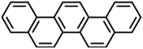
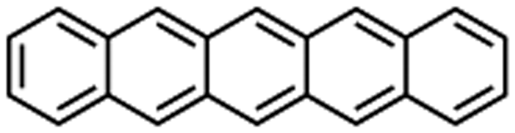
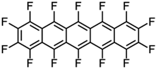

 represents the potential energies of electrons without electron–electron interaction, and
  the potential energies of the interacting N-electrons in the crystal. Hereafter we omit summation for N electrons in the crystal (p1, p2,…, pN; r1, r2,…,rN) for simplicity and describe the potential energy terms with V. We chose ϕ(ri) = 0 from possible selection of gauge function for zero current and charge system, put p·A = 0 by neglecting strong surface induced phenomena and furthermore neglect A2 term which is much smaller than the p·A term, giving

 for ℏωkp photons because of a mathematical convenience. For radiations of various ℏωkp, the vector potential is rewritten, because it is real quantity, as
 and annihilation (akpγ) operator and describe Hrad as given in eqn (2c).38 The operators
 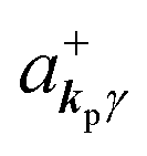 and akpγ are directly related to the vector potential A of the radiation in a crystal with an ωkp- and kp-dependent dielectric constant [εr(ωkp,kp)] as
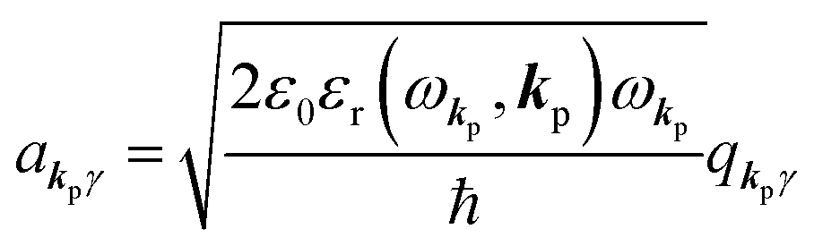
 and akpγ, He,rad is given as
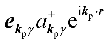 operate on the eigenfunction of the radiation. Hereafter we use the dipole approximation, eikp·r ≅ 1, and write unperturbed Hamiltonians for the electron and the photon system as H0e and H0rad, respectively, in the following discussion.
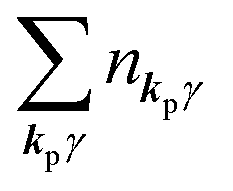 at unit volume) by |n11, n12, n21, n22,…,nkpγ,…〉, where the total photon number is
 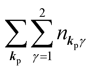 at unit volume and we write this as
  in the following equations. These unperturbed systems and the non-interacting electrons-and-photon coexisting system satisfy following equations:
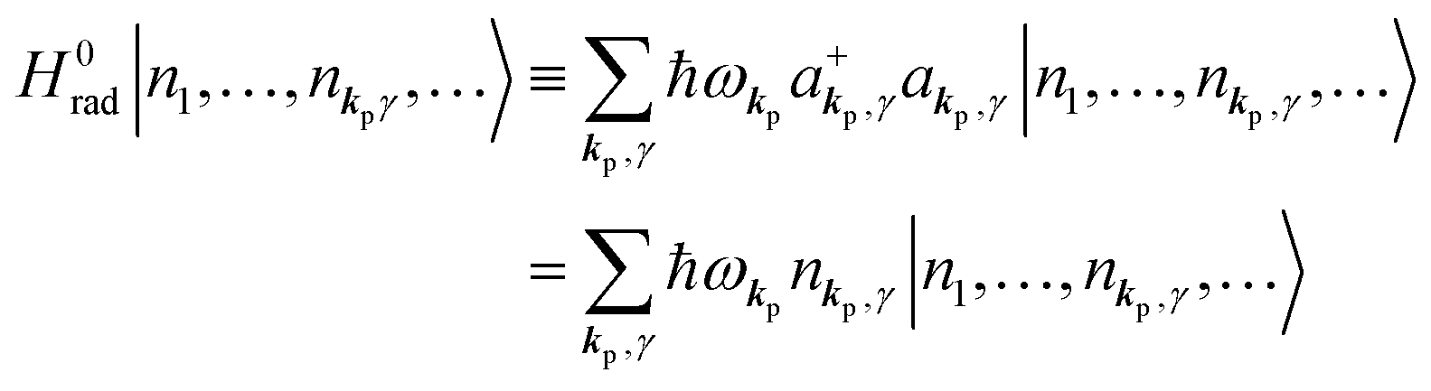
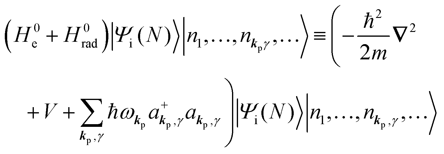
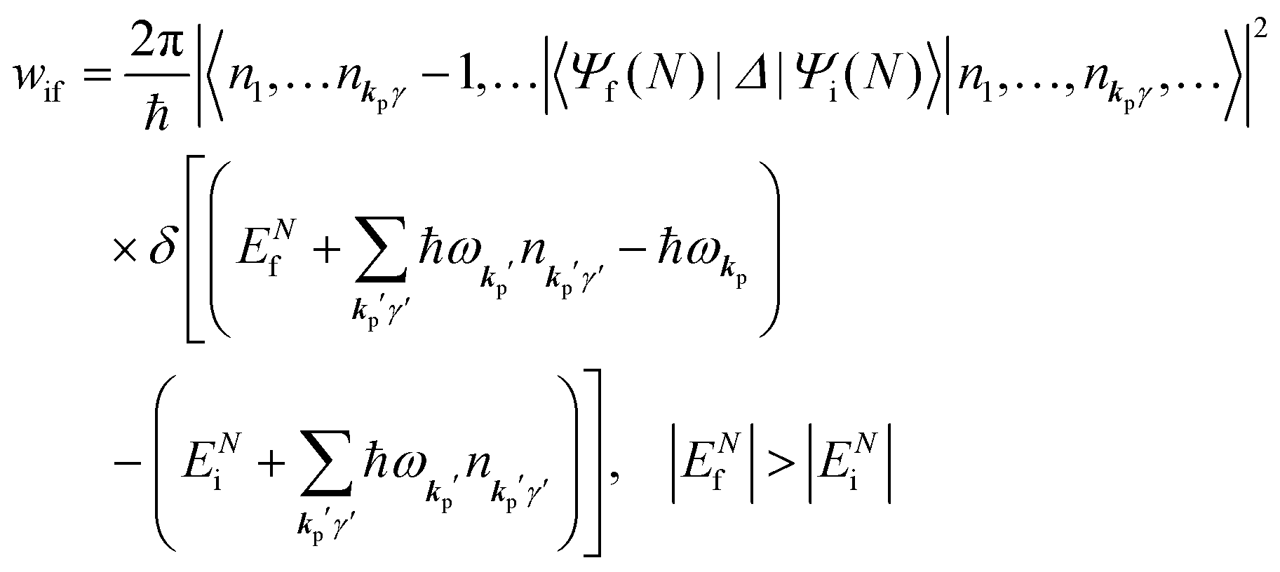
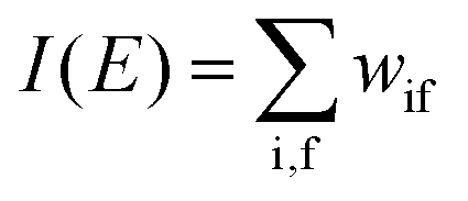
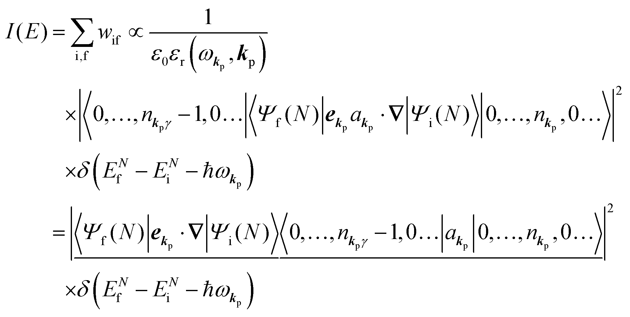
 and thus the final state becomes |Ψf(N)〉|0,…, nkpγ + 1, 0…〉.
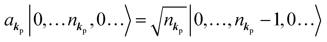 , we obtain following relation for the total photon number
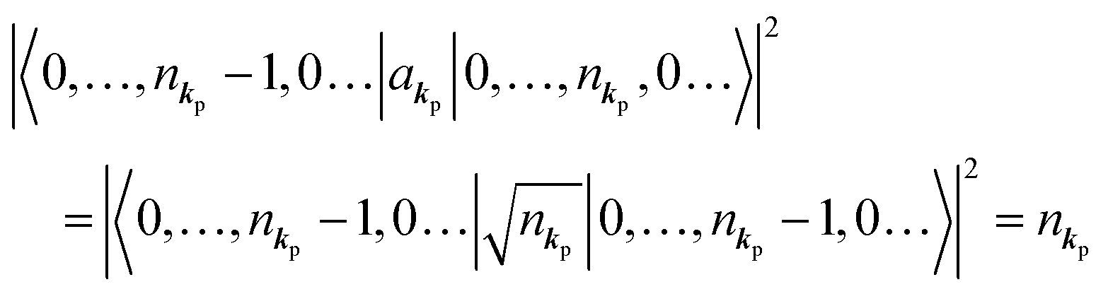
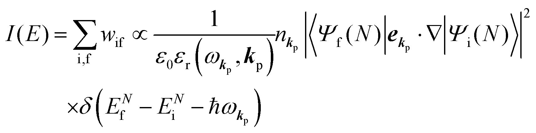
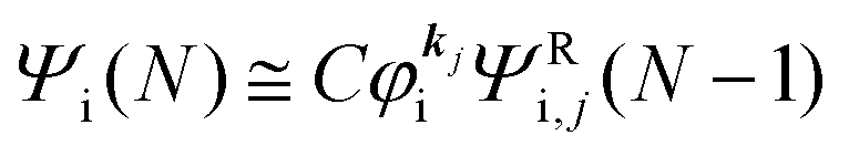
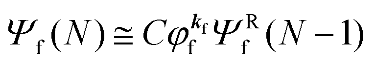
 is the initial j-th one-electron band specified by the electron momentum ℏkj or the initial j-th molecular orbital (MO) level specified by a set of atomic orbital coefficients that corresponds to the kj value,46–48 from which the photoelectron is excited. ΨRi,j(N − 1) is the residual (N − 1) electron wave function after separation of the j-th state
  as written in eqn (12a), C an antisymmetric operator which antisymmetrizes the N-electron wave function, and i stands for initial state and R for remaining (N − 1) electrons.
  is the wave function of the photoelectron of momentum ℏkf, which is similar to the time-inverted wave function of low-enrgy electron diffraction (LEED) with the scattering state boundary condition49,50 and ΨRf(N − 1) the wave function of the remaining (N − 1) electron final state. Both of ΨRi,j(N − 1) and ΨRf(N − 1) are not expressed by one-electron wave functions as there are electronic interaction (correlation) in residual (N − 1) electrons system. The structure of ΨRi,j(N − 1) depends on
 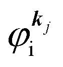 , and ΨRf(N − 1) should have large impacts of photogenerated “hole” and therefore involves unknown energetic excitation such as creation of phonons, polarons, and changes in other electronic energies after the hole creation. Therefore ΨRi,j(N − 1) and ΨRf(N − 1) are in general discussed based on many-particle theory.38,41,44 Here we consider such various states for ΨRf(N − 1) specified formally by s. We then write

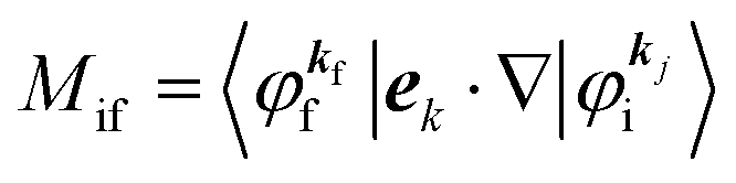

 for simplicity till they become necessary. A(k,E) describes energy and k dependent density-of-stales [ρ(E,k)] owing to electron correlation, which will be discussed later again. Here and after we use following symbols for the initial (i) and the final (f) state related electron energies:
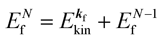 , where
  and EN−1f are the photoelectron kinetic energy and the remaining (N − 1) electrons energy, respectively;
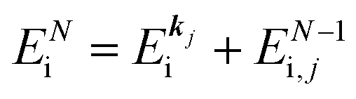 , where
 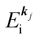 and EN−1i,j are the Hartree–Fock orbital energy of the j-th state or at momentun ℏkj of the j-th band and the energy of the remaining (N − 1) electrons at the absence of the one j-th state electron, respectively;
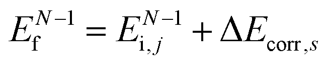 , where ΔEcorr,s (≡ ΔEcorr) is the correlation energy; and
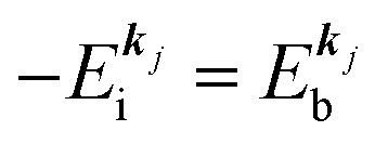 , where
  is the binding energy of the j-th level or the j-th band at momentun kj.
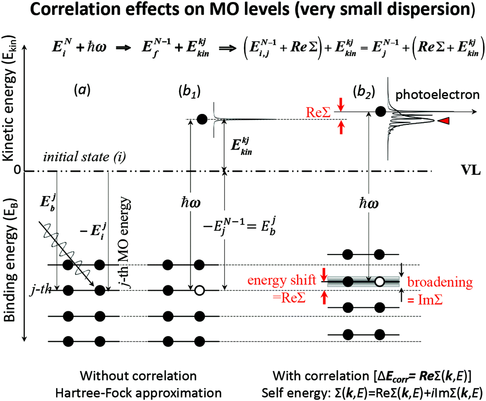
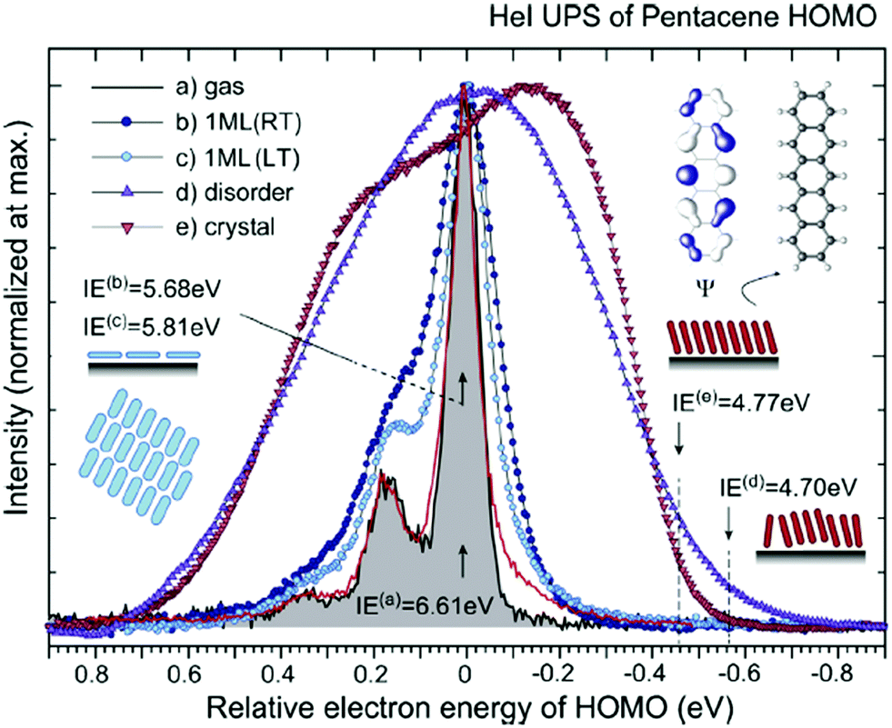


 ) [see Fig. 1(a, b1) and 3(b)],
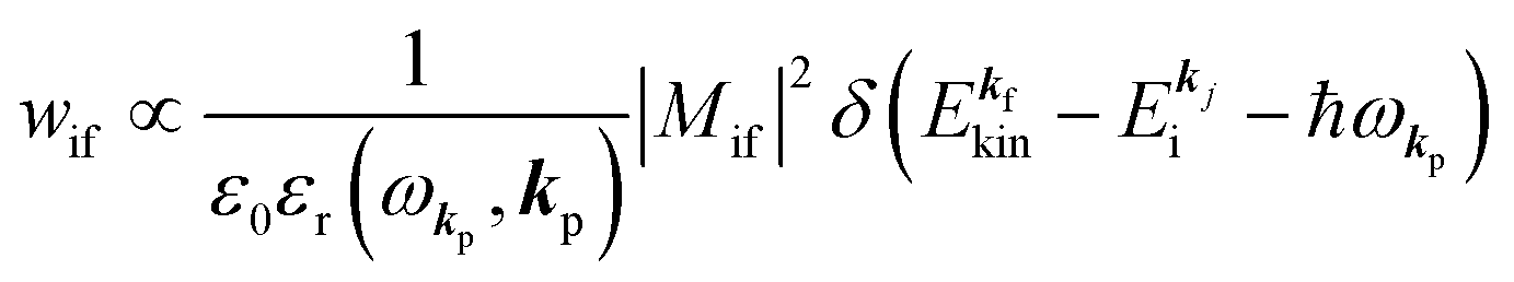
 is the kinetic energy of photoelectron and
  the one electron Hartree–Fock energy of the initial j-th state
  , both of which refer the vacuum level here.
  is equal to the binding energy
 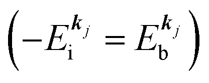 measured from the vacuum level (see Fig. 1), as we assume that the other Hartree–Fock orbitals do not change upon photohole creation at
  and there is no electronic correlation (the Koopman's theorem58,59). It is of note again that the photoexcitation of the electron must satisfy k conservation, although it is not explicitly written in eqn (17). This offers a simple picture to photoelectron spectra, where peaks observed in a photoelectron spectrum originate from electrons in the orbital/band
  at the binding energy
  . In other words, ‘they’ are photoexcited to the continuum state
  to emit a photoelectron with the kinetic energy of
  , and therefore eqn (17) tells that the photoelectron peaks offer a set of energies of occupied levels [see Fig. 1 and 3(b)].
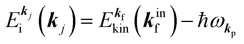 and using the momentum conservation of the photon and electron system inside of the crystal,
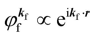 .60,61 One needs to recall that a photoelectron travels at least in the attractive force produced by the Coulomb potential of the photogenerated ion/hole, and therefore its wavefunction cannot be described with a plane wave, as the plane wave is an eigenfunction of a free electron moving in ‘vacuum’. In order to describe the photoelectron inside and outside of a solid, the above eikf·r is modified to involve spherical waves produced by scattering with various Coulomb potentials inside and outside of the solid. The correct photoelectron wave function then reaches eikf·r at r → ∞, at which the Coulomb potentials become zero. As the use of a plane wave for
  does not impact photoelectron kinetic energy with respect to the vacuum level (defined at r → ∞), it is possible to discuss about results based on the energy conservation of photoemission but not possible to discuss intensity related phenomena because the phase of the photoelectron wave does change due to the scattering and interference effects thus impact on the intensity. The use of incorrect photoelectron wave function leads wrong results of angular distribution of photoelectron. However, the use of the plane-wave approximation can offer a large benefit for direct understanding of what photoelectron spectroscopy offers to us, if one does not discuss the spectral intensity and its angular distribution at high accuracy. The photoelectron spectrum I(E) becomes at the plane wave approximation to
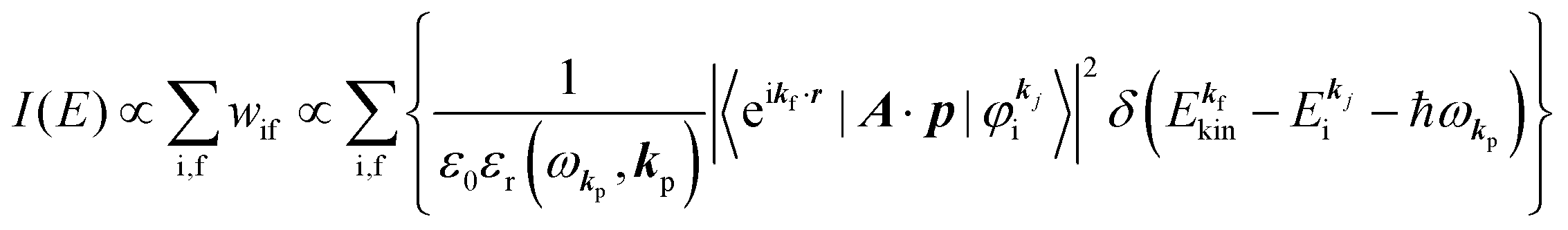
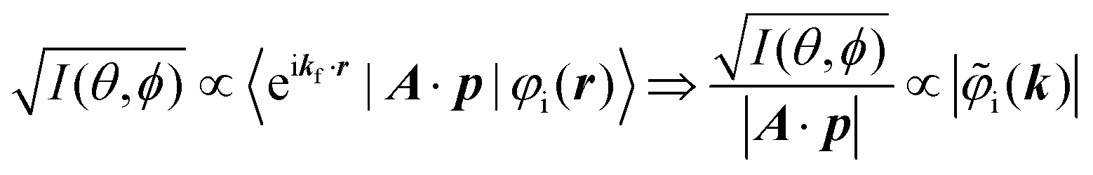
 . This method is known as molecular orbital tomography for direct mapping of un-visible molecular wave functions using ARUPS.68,69,71 It is of note that the phase symmetry of MO was also measured by using circular polarization of incidence photons,70 although the phase information of the MO disappears by photoelectron spectroscopy measurements using linearly polarized photon because the spectrum is given by the square of the transition matrix element (|Mif|2).
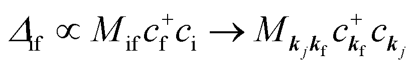 , at conservation of the wavevector upon i (the initial kj state) → f (the final kf state) transition with kj = kf,
 and ckf the one electron creation and annihilation operator with the wave vector kf, respectively, and so on. Here
  runs over the first Brillouin zone with momentum conservation kj (the j-th orbital/band of the initial state) = kf (the final state). Subscripts f and i of the energies in δ function are read as kf and kj, respectively, if necessary, or kf and kj may be replaced by f (final state) and i (initial state) for simplicity. We then rewrite eqn (21) to have following relation,
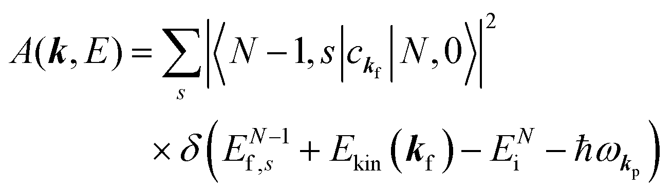
 . We used following relations to relate with the writing method before this section,
 (one electron with kj is added)

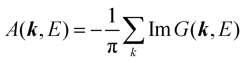
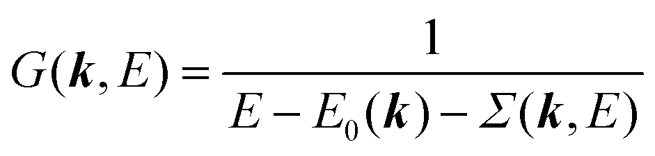
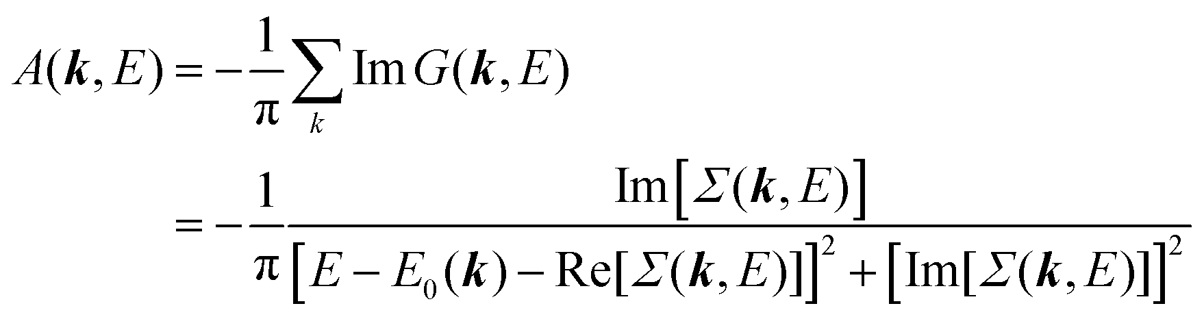

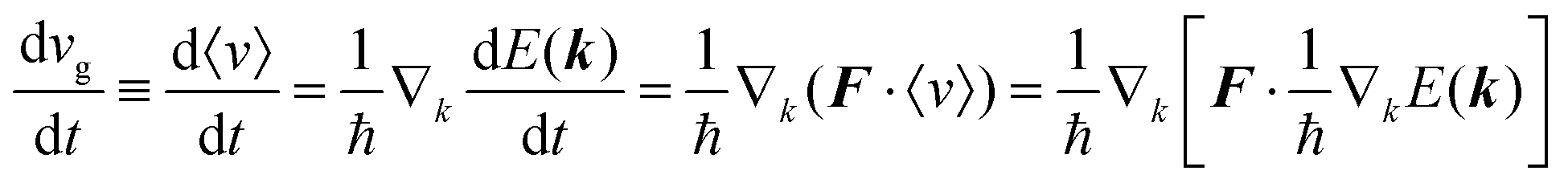


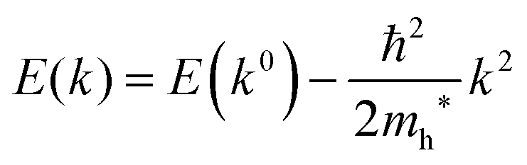

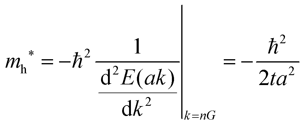
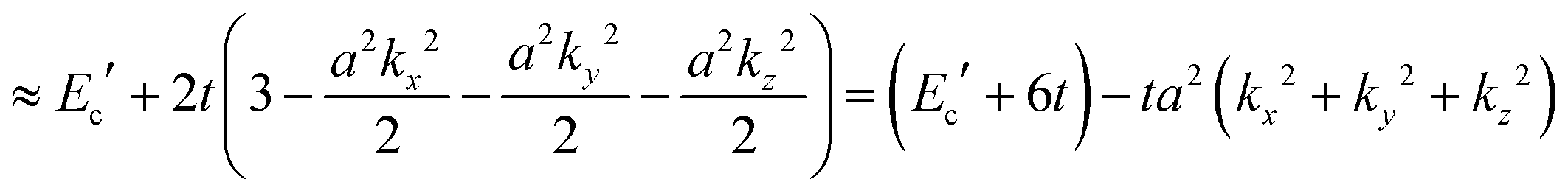
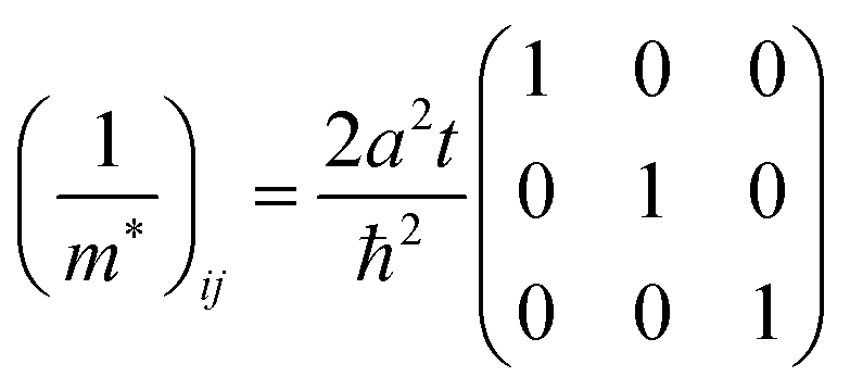
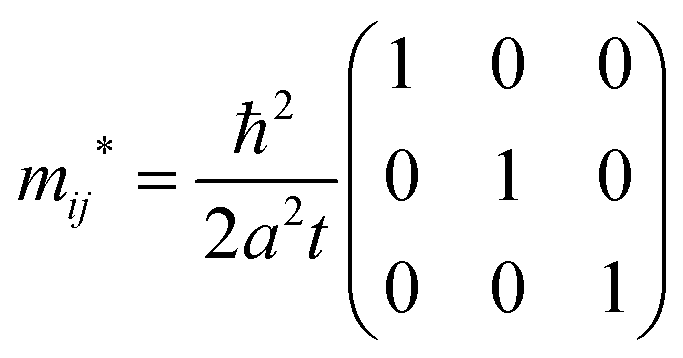
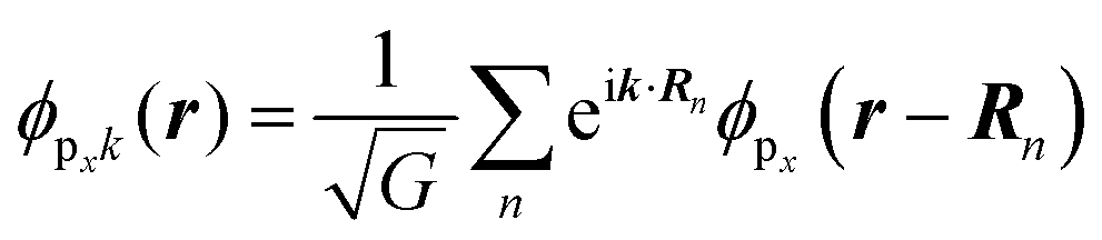 in SC, where ϕpx(r) ≡ ϕp(r)x and
  is the normalization constant.

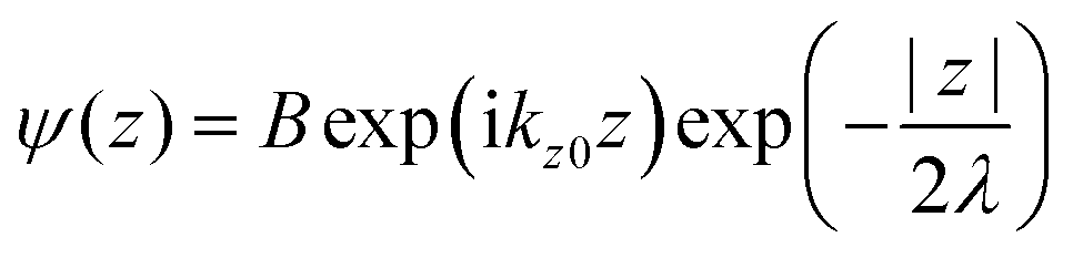
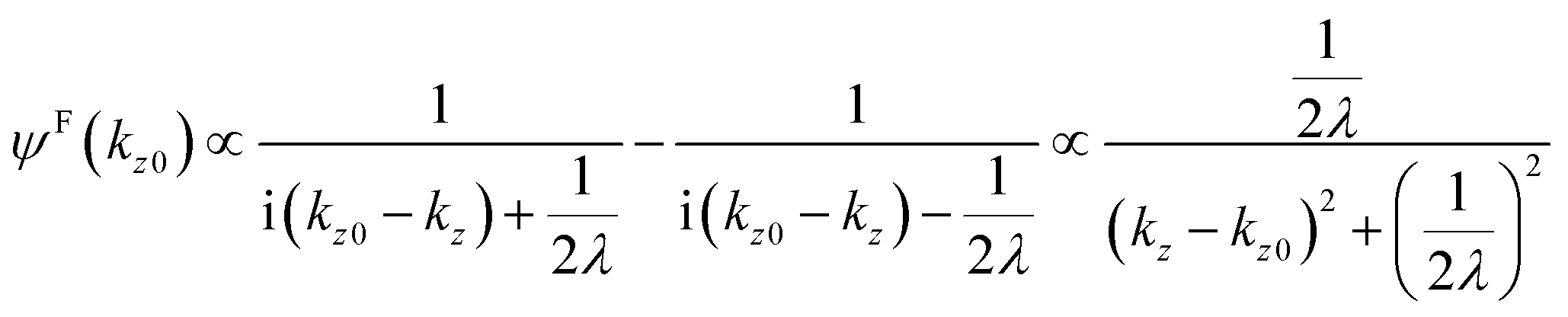
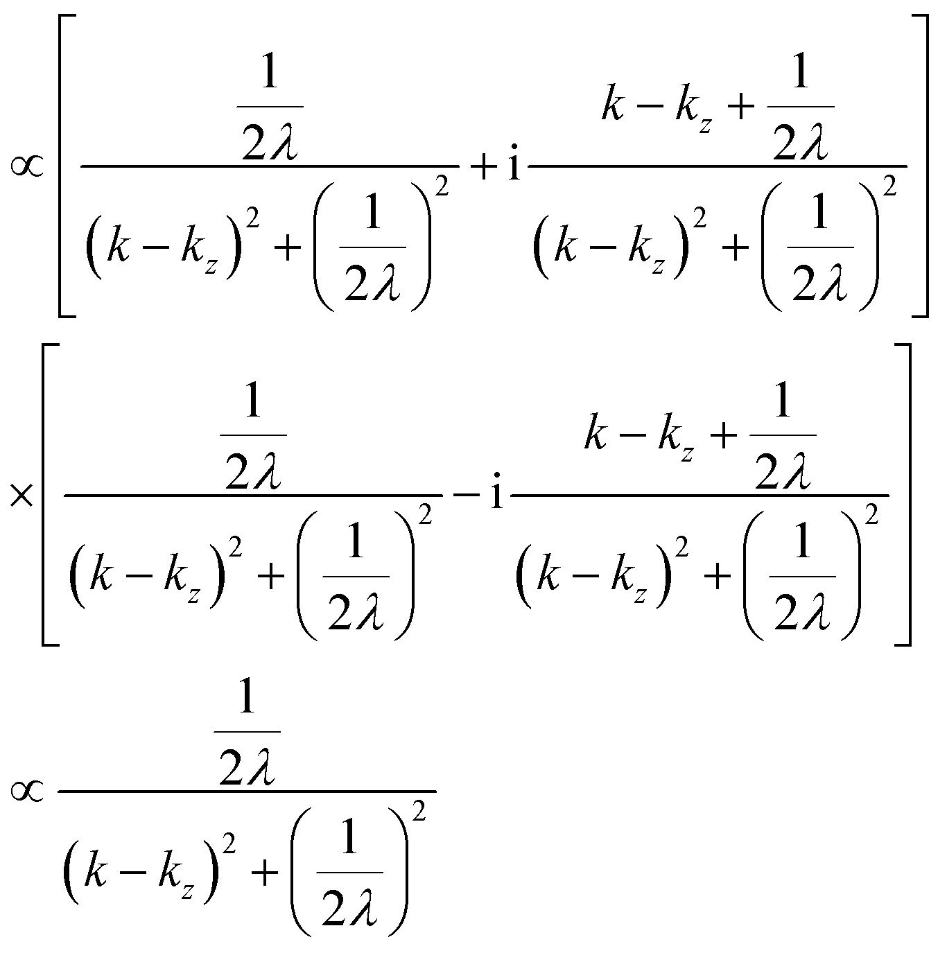

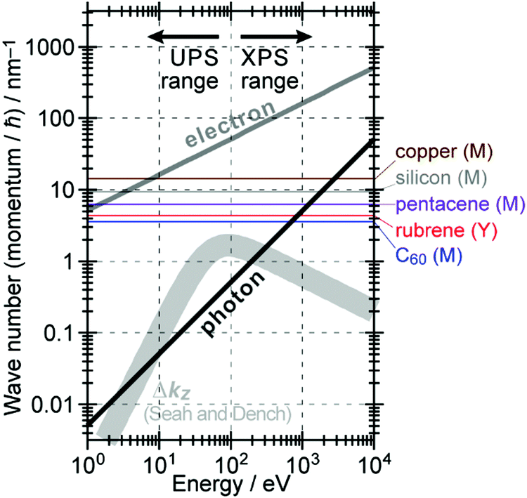


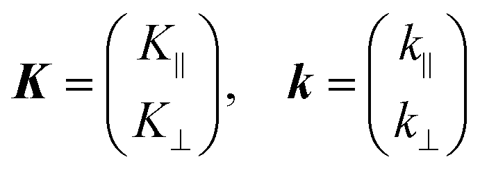
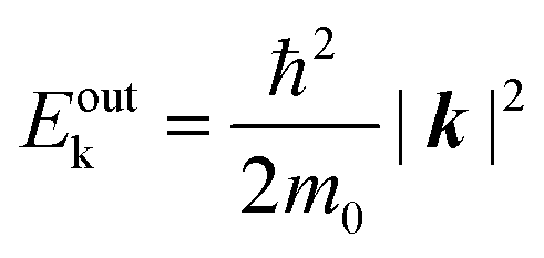
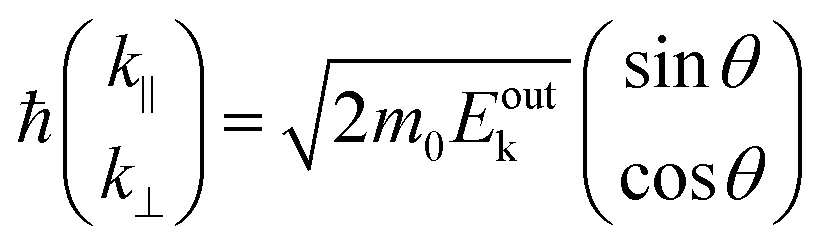
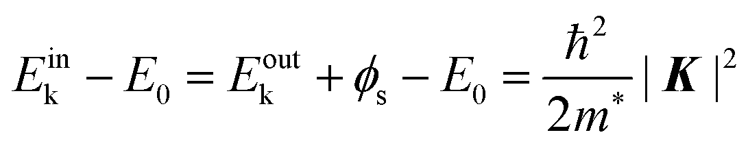
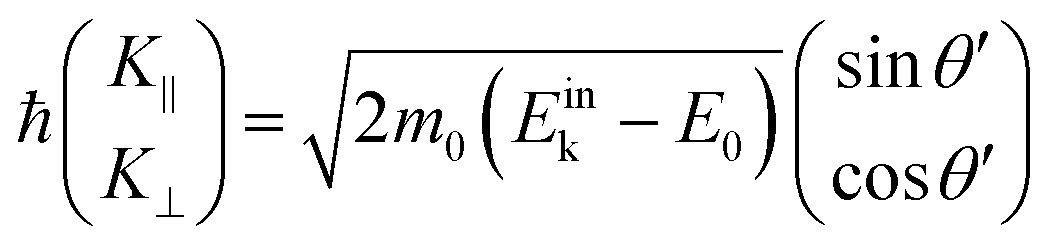

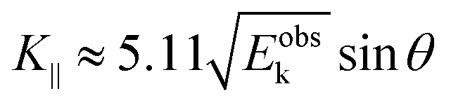
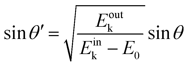

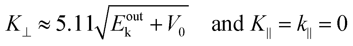

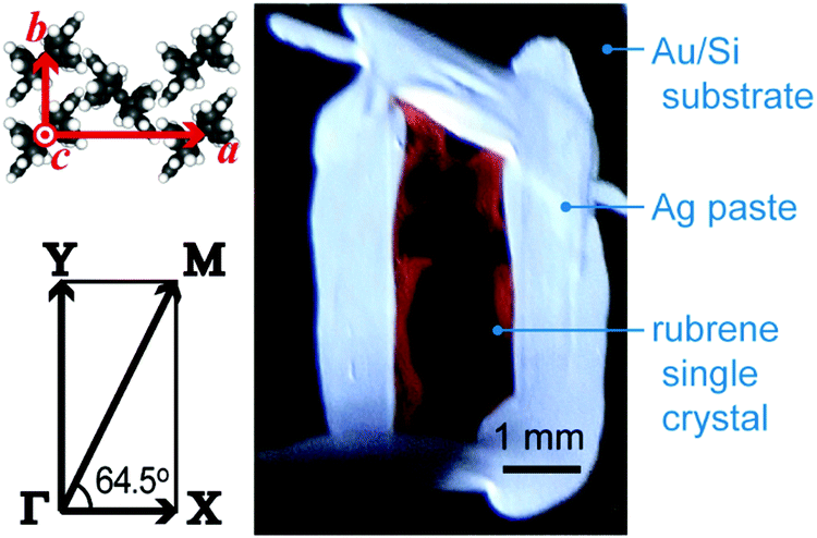
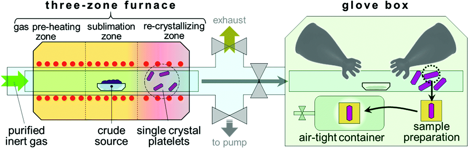
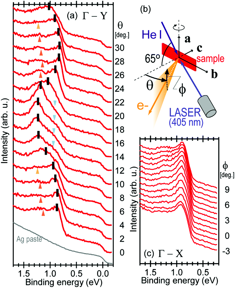


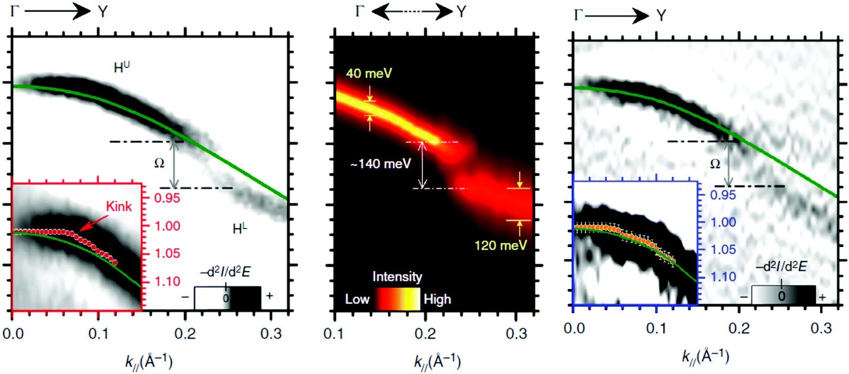
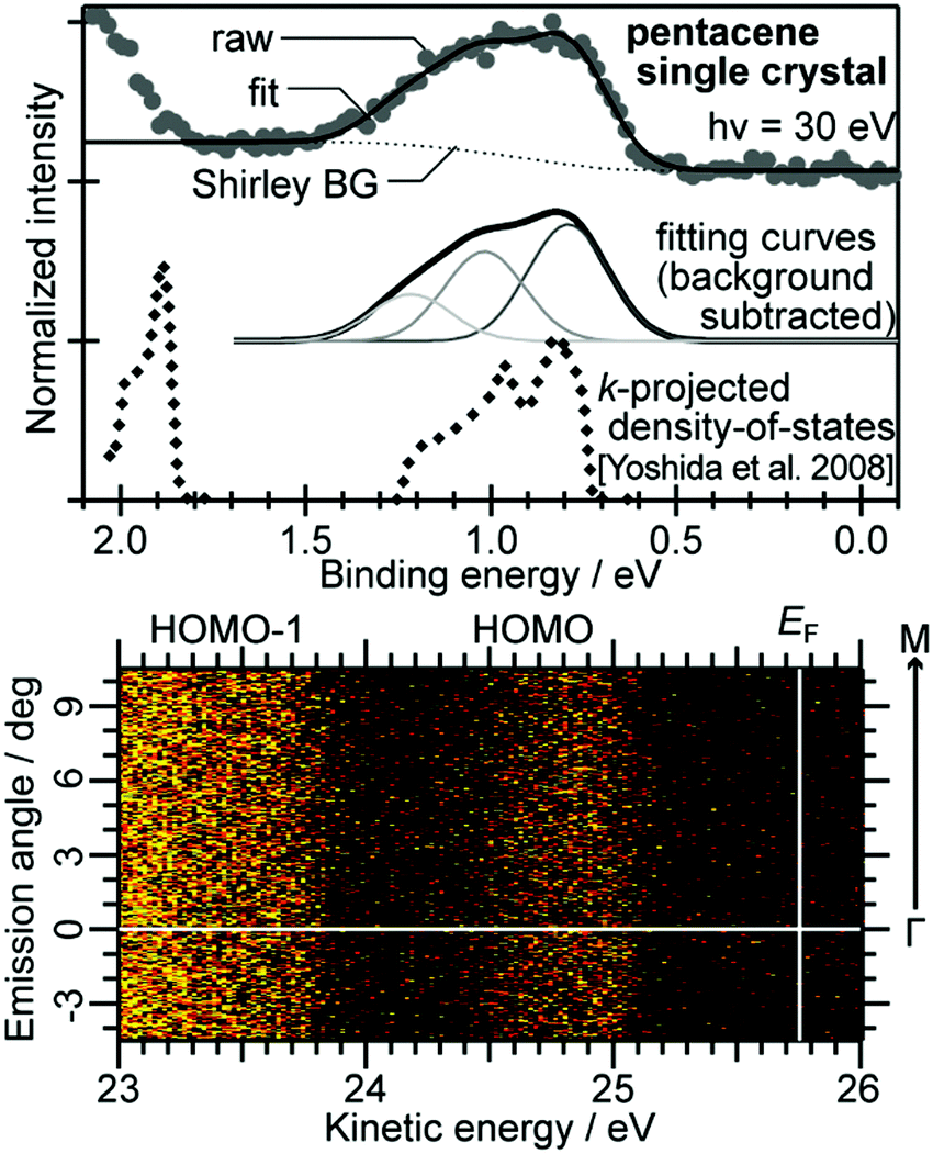
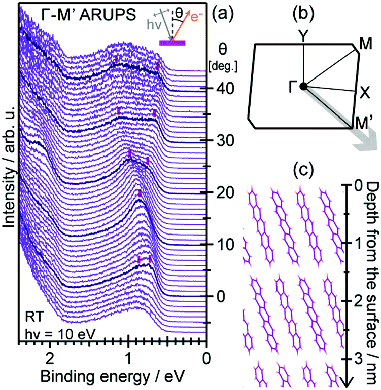
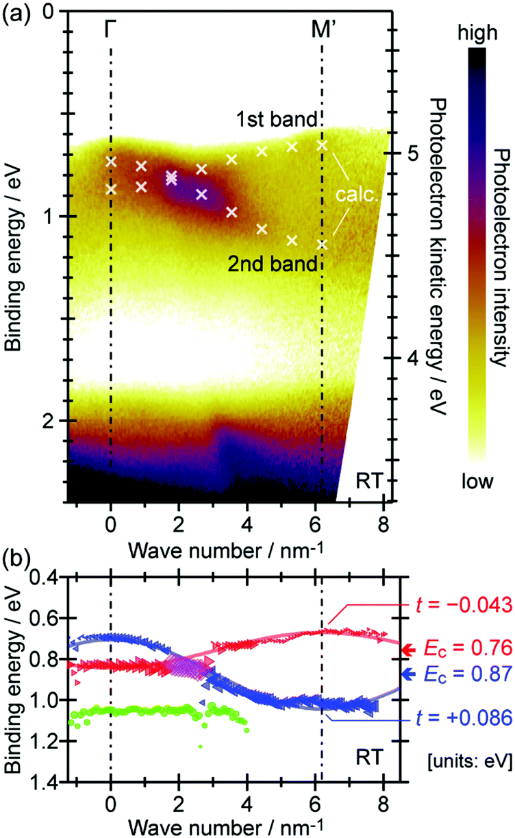
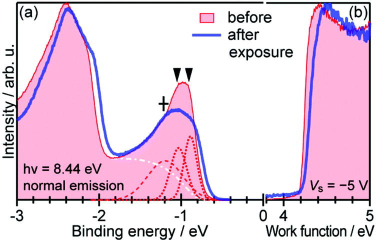
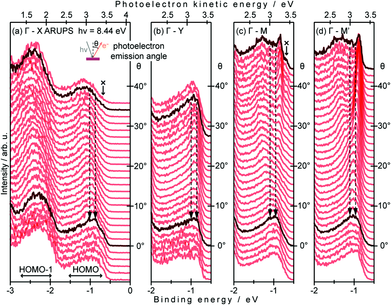
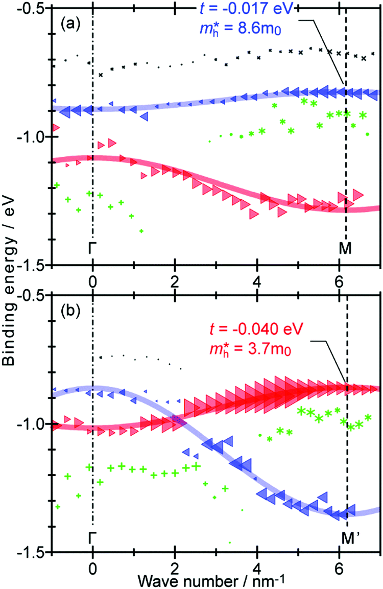
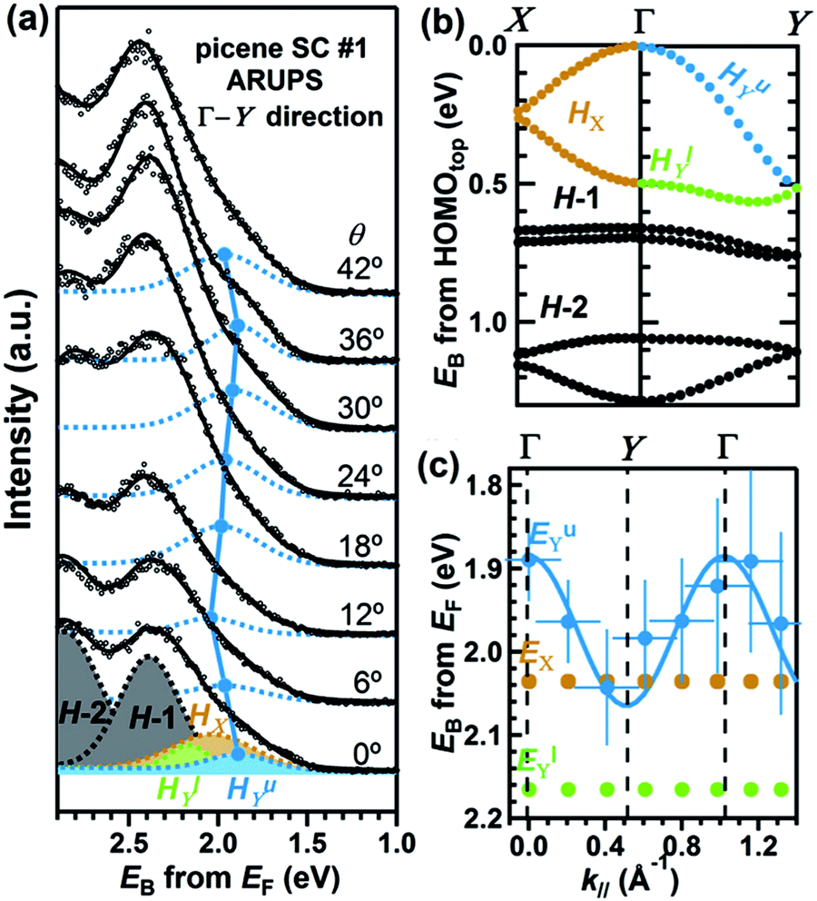
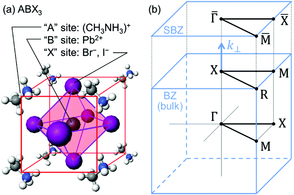
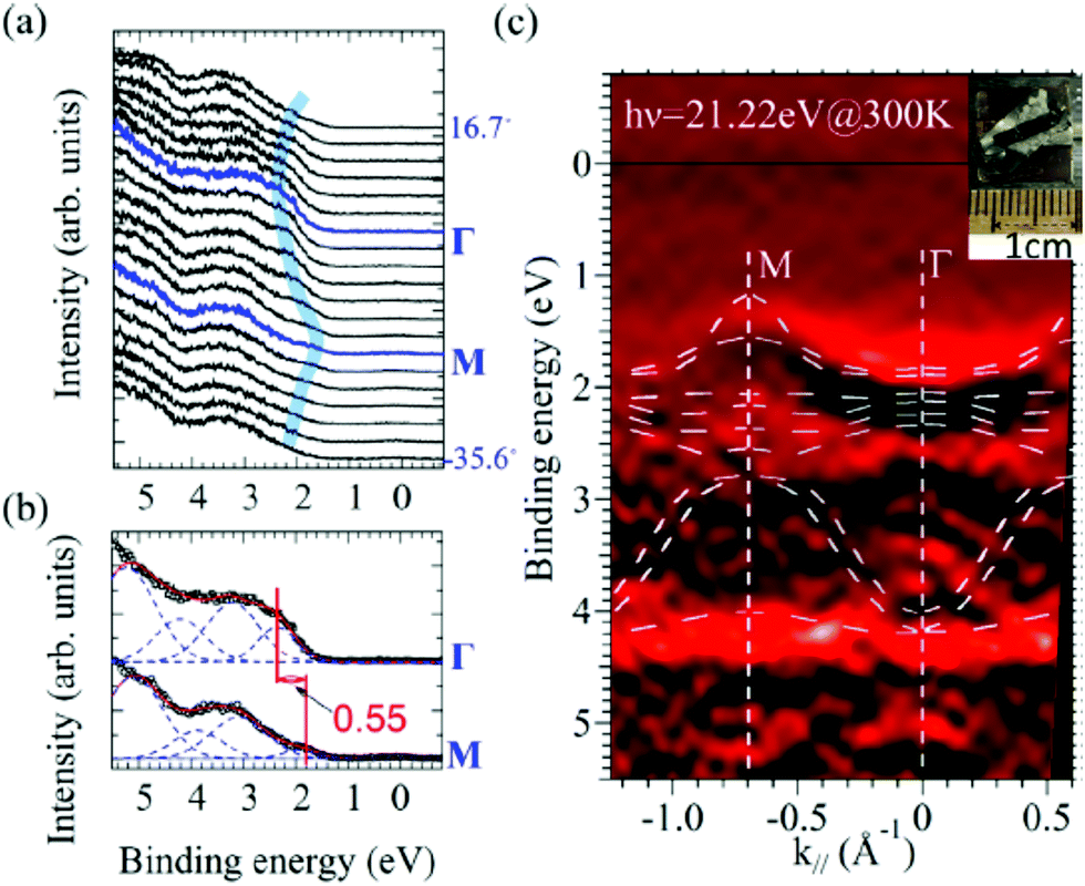


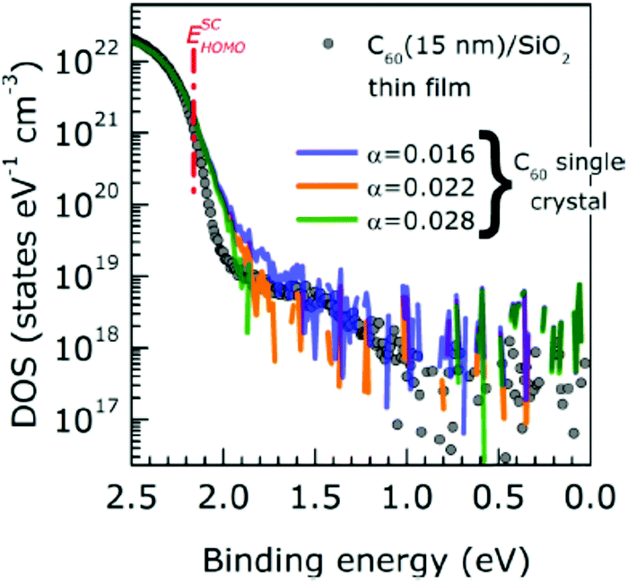

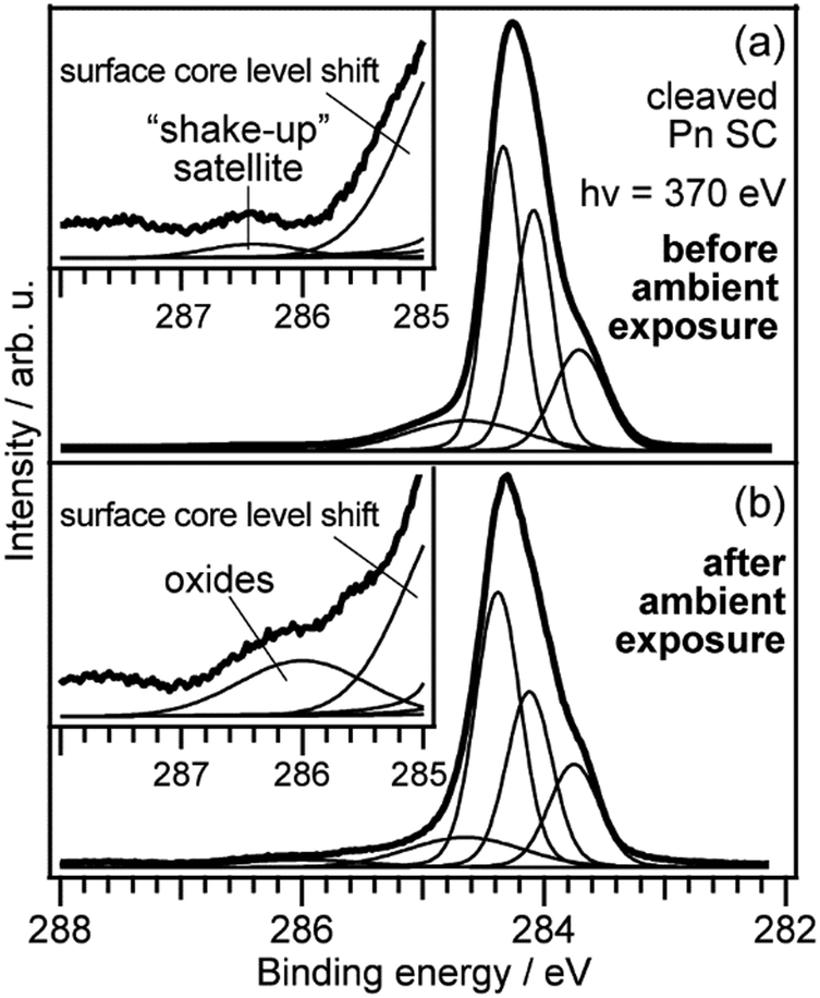
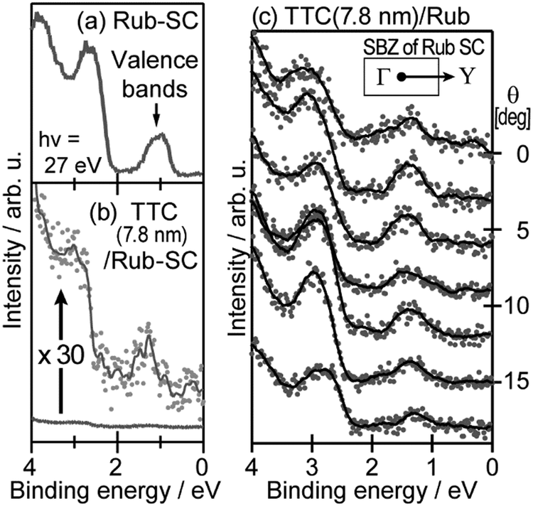
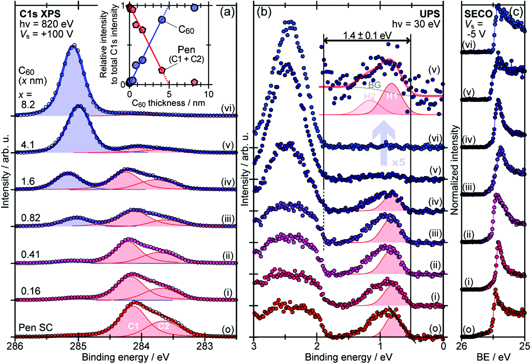
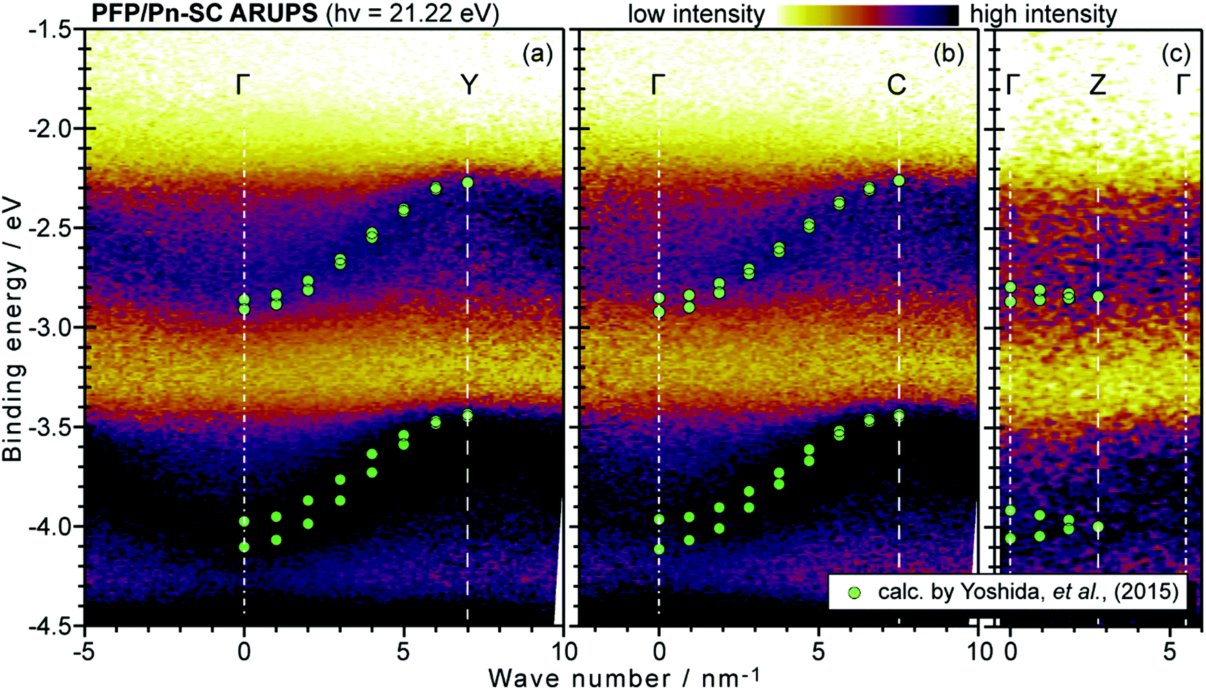
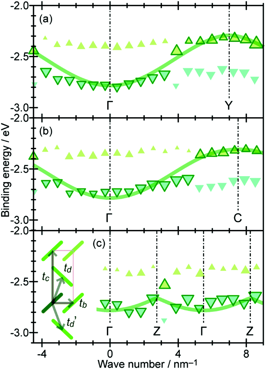
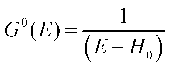
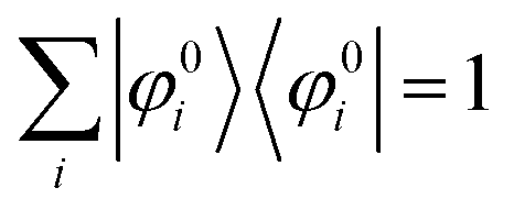
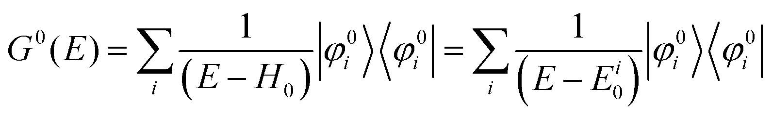
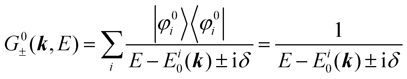
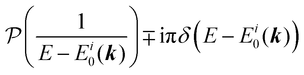


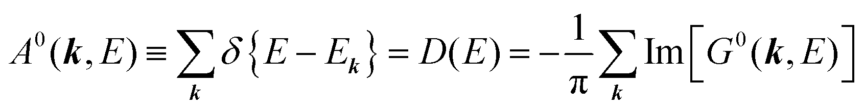
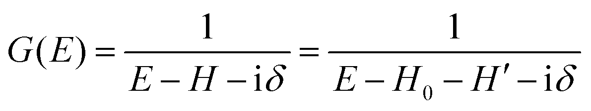


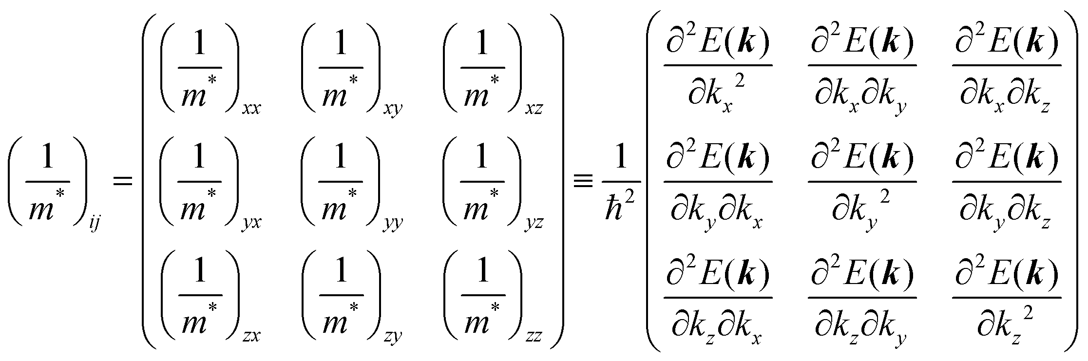
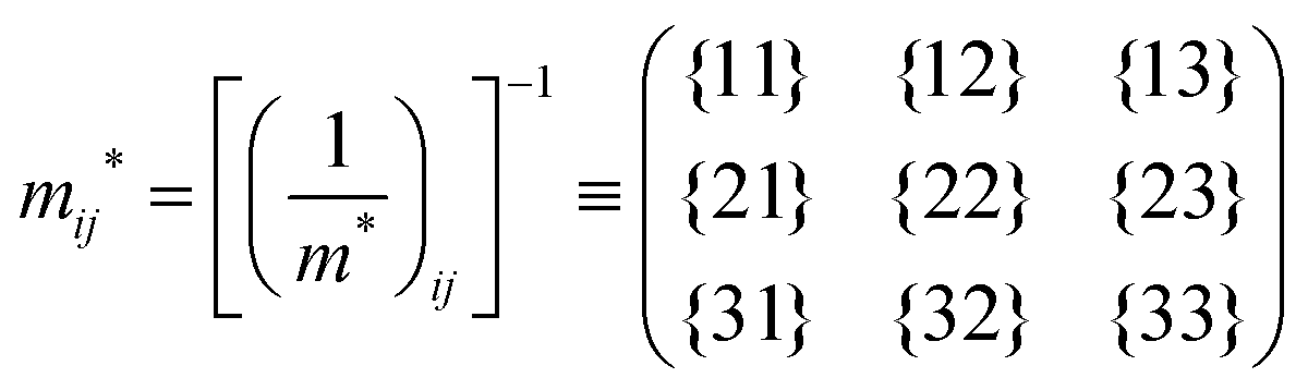
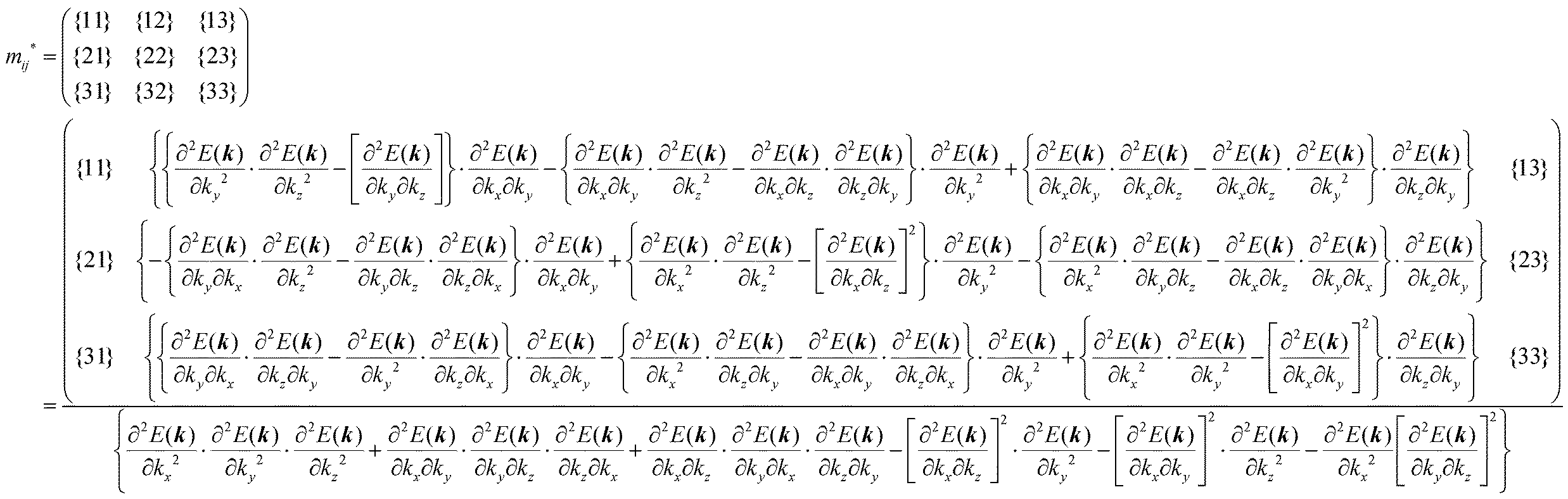
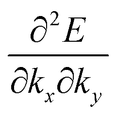 etc. If the dispersions are the same along the three main axes, off-diagonal elements disappear. If the off-diagonal elements do not disappear, it is very difficult to obtain accurate effective masses along such off-diagonal related directions. Moreover, we cannot measure mij* (for i ≠ j) of the hole (electron) selectively with ARUPS (ARIPES) experiments.