
 Open Access Article
 This Open Access Article is licensed under a
 Creative Commons Attribution 3.0 Unported Licence
Liquid phase exfoliation of MoS2 and WS2 in aqueous ammonia and their application in highly efficient organic solar cells†
Begimai
Adilbekova
 a,
Yuanbao
Lin
a,
Emre
Yengel
a,
Hendrik
Faber
a,
George
Harrison
a,
Yuliar
Firdaus
a,
Abdulrahman
El-Labban
a,
Dalaver H.
Anjum
b,
Vincent
Tung
a and
Thomas D.
Anthopoulos
*a
a,
Yuanbao
Lin
a,
Emre
Yengel
a,
Hendrik
Faber
a,
George
Harrison
a,
Yuliar
Firdaus
a,
Abdulrahman
El-Labban
a,
Dalaver H.
Anjum
b,
Vincent
Tung
a and
Thomas D.
Anthopoulos
*a
aKing Abdullah University of Science and Technology (KAUST), KAUST Solar Center (KSC), Thuwal 23955, Saudi Arabia. E-mail: thomas.anthopoulos@kaust.edu.sa
bKhalifa University, Department of Physics, Abu Dhabi, United Arab Emirates
First published on 16th March 2020
Abstract
Simple, scalable and cost-effective synthesis of quality two-dimensional (2D) transition metal dichalcogenides (TMDs) is critical for fundamental investigations but also for the widespread adoption of these low-dimensional materials in an expanding range of device applications. Here, we report on the liquid-phase exfoliation (LPE) of molybdenum disulfide (MoS2) and tungsten disulfide (WS2) in aqueous ammonia (NH3(aq.)) as a greener alternative to commonly used but less environmentally friendly solvents. The synthesized nanosheets can be prepared in high concentrations (0.5–1 mg mL−1) and exhibit excellent stoichiometric and structural quality with a semiconducting character. These characteristics make them ideal for application in organic optoelectronics, where optical transparency and suitable energetics are two important prerequisites. When MoS2 and WS2 are used as the hole transport layer materials in organic photovoltaics, cells with a power conversion efficiency of 14.9 and 15.6%, respectively, are obtained, highlighting the potential of the aqueous ammonia-based LPE method for the preparation of high quality TMDs. The method could potentially be extended to other TMDs.
Introduction
In the last decade, two-dimensional (2D) materials have attracted enormous interest owing to their atomically thin geometry and appealing optical, mechanical and electronic properties.1,2 Among these materials, semiconducting transition metal dichalcogenides (TMDs) have received the most attention as promising candidates for applications in nanoelectronics and optoelectronics.3–6 This class of materials is formed by a hexagonal layer of transition metal atoms from group IV–VI sandwiched between two chalcogen atoms.7,8 Adjacent layers of TMDs are stacked via weak van der Waals forces.1,9 Breaking these weak interactions allows the thinning of bulk TMDs down to mono- and/or few-layers.9 In the literature, several top-down and bottom-up methods such as mechanical cleavage, liquid-phase exfoliation (LPE) and chemical vapour deposition (CVD) have been proposed to synthesize these 2D layers.1,3,7–10 Among them, LPE is found to be the simplest and most cost-effective one.5,11,12The most attractive feature of the LPE process is that it yields suspensions of TMD nanosheets, which enables easy growth of thin films by filtration, inkjet printing or spin-coating.5,7,9,13 The LPE process can be performed either by ion intercalation or sonication, where the former process is characterised by drawbacks such as defect formation, long process times and sensitivity to ambient conditions.1,3–5,14 On the other hand, sonication is a relatively mild and scalable method, where a powder of the desired material is subjected to ultrasonic waves in an appropriate solvent.2,4,7,13 Ultrasonic waves produce cavitation bubbles or shear forces, which separate the layered materials into mono- to few-layer nanosheets.5,9 The yield and stability of this process depend on various parameters, with the solvent selection being a critical one.2,7,12,15
There are several parameters that are proposed as solvent selection criteria, including the Hildebrand solubility, Hansen solubility and surface tension, due to the fact that the solvent selection impacts the process of LPE in a significant way.12,16 Yet, surface tension matching between the solvent and TMDs was found to be the easiest and most direct way to select the most efficient solvent and to explain the successful exfoliation process.16 A sufficient surface tension match is a key requirement to minimize the energy needed for breaking the van der Waals forces between layers.9,15,16 Since the surface tensions of MoS2 and WS2 were estimated to be 46.5 and 40 mJ m−2, respectively, for successful exfoliation of these materials the solvent has to be chosen to have a surface tension matching the surface tension of the materials.5,15 Although LPE of TMDs has been explored in various solvents such as N-methyl-2-pyrrolidone (NMP), N-cyclohexyl-2-pyrrolidone (CHP), isopropanol (IPA), ethanol and even water, the number of environmentally friendly solvents often used is still very limited.3,4,7 Despite the high exfoliation efficiency in NMP and CHP, their boiling points above 200 °C limit their more widespread applications.4,9,11 Even though water can be used for the exfoliation of layered materials, it has some limitations such as long process times and the need for elevated process temperatures.17 These difficulties are associated with the large surface tension mismatch at room temperature, where water has a surface tension of 72 mJ m−2.18 On the other hand, the surface tension of NH3(aq.) (50% v/v) is ≈49 mJ m−2 and enables the efficient exfoliation of TMDs with similar surface tensions. In comparison with water-only exfoliation, the aqueous ammonia method offers important advantages such as shorter sonication times, higher yield, and improved suspension stability even at low temperatures.
Here, we focused on the LPE of MoS2 and WS2 in NH3(aq.). We show that the LPE process yields dispersions containing monolayer and multilayer nanosheets with lateral sizes ranging between tens and hundreds of nanometres for both MoS2 and WS2. In addition to the successful exfoliation, the low boiling points of NH3 and water make NH3(aq.) more favourable than NMP or CHP, which require high-temperature post-deposition annealing. Furthermore, the oxidizing property of NH3(aq.) allows increasing the hydrophilicity of surfaces.19 The physical properties of the exfoliated nanosheets were characterised via a range of techniques including Raman, UV-vis, photoluminescence (PL), X-ray photoelectron spectroscopy (XPS), and ultraviolet photoelectron spectroscopy (UPS). The morphological and structural properties of the nanosheets were also investigated using atomic force microscopy (AFM) and high-resolution transmission electron microscopy (HR-TEM). To demonstrate the good electrical properties of the exfoliated MoS2 and WS2 nanosheets, we utilised them as a hole transport layer (HTL) in organic solar cells (OSCs), yielding devices with a power conversion efficiency (PCE) of 14.9% and 15.6%, respectively.
Results and discussion
LPE preparation of 2D TMDs was performed via sonication of MoS2 and WS2 powders in NH3(aq.) (50% v/v) followed by a centrifugation step to remove bulk aggregates, as illustrated in Fig. 1a. The TMD concentrations within the respective supernatants were determined by filtration and weighing and were found to be ≈0.5 mg mL−1 for MoS2 (prepared at 6000 rpm) and ≈1 mg mL−1 for WS2 (prepared at 4400 rpm). The yield of the process was estimated at ≈16% (0.5 mg mL−1) and ≈25% (1 mg mL−1) for MoS2 and WS2, respectively. All resulting dispersions of MoS2 and WS2 nanosheets in NH3(aq.) exhibit the Tyndall scattering effect (Fig. 1a) upon exposure to a laser beam (532 nm), proving the presence of a fine suspension.20 When stored at room temperature both TMD suspensions remain stable for up to a week. However, keeping them at 5 °C extends the storage lifetime to months provided that the vial remains well sealed so the ammonia does not leak. | ||
| Fig. 1 (a) Schematic illustration of the LPE process. TDM powders are placed in a vial with aqueous ammonia followed by the ultrasonication and centrifugation steps. The photo shows the pronounced Tyndall effect of the resulting nanosheet suspensions. (b) UV-vis absorption spectra of the MoS2 and WS2 suspensions. Raman spectra of MoS2 (c) and WS2 (d) nanosheets spin-coated onto Si2+/SiO2 substrates. AFM images and corresponding line scans of various MoS2 (e and g) and WS2 (f and h) flakes on Si2+/SiO2 substrates. | ||
The UV-vis absorption spectra of MoS2 and WS2 dispersions (Fig. 1b) show two distinct peaks, so-called A and B excitons, attributed to direct interband excitonic transitions.21–23 They are located at ≈670 and ≈608 nm for MoS2 and ≈625 and ≈520 nm for WS2. These characteristic peaks provide an indication of the well-dispersed nature of MoS2 and WS2 nanosheets in NH3(aq.) that have a 2H crystal structure.14,23 Also, we confirmed the semiconducting nature of the nanosheets by PL measurements, further supporting this assertion (Fig. S1, ESI†).1,24,25
To further investigate the efficiency of the proposed LPE route and determine the thickness of the resulting nanosheets, we employed Raman spectroscopy and AFM. The Raman spectra for MoS2 and WS2, obtained using 532 nm excitation, are shown in Fig. 1c and d. Both materials showed two first-order peaks assigned as E12g and A1g arising from the in-plane and out-of-plane vibrations, respectively.6,21,22,26 Apart from these peaks, WS2 showed a strong second-order longitudinal acoustic mode (2LA) overlapping with the E12g mode, originating from the lattice vibration and electronic band structure coupling.6 The position (frequency) of these modes is correlated with the thickness of TMDs.7,21,23,26,27 Consequently, the frequency difference between these two modes can be used to estimate the layer number of exfoliated TMDs.14,26 For our TMDs, we observed a blue shift of the A1g mode and a red shift of the E12g mode, which is caused by the reduction of interlayer interactions.6,11,26 The Raman spectra of two MoS2 nanosheets (Fig. 1c) exhibit a frequency difference of ≈24.4 cm−1 and ≈24.5 cm−1, presumably denoting the presence of four and five monolayers, respectively.21,28 For WS2 nanosheets (Fig. 1d), we observed frequency differences of around 63 cm−1 and 65 cm−1, indicative of monolayer and bilayer flakes, respectively.6
AFM measurements were performed to confirm the formation of few-layer nanosheets and investigate their physical characteristics such as size and shape. As can be seen from Fig. 1e and f, the lateral size of both MoS2 and WS2 nanosheets varies from tens to hundreds of nanometres. The height profile images of selected MoS2 nanosheets in Fig. 1g (L refers to the layer number, e.g. 2L means 2 layers) revealed a height ranging between 2 and 8 nm, which corresponds to 2–6 layers. In contrast, the height profile of WS2 (Fig. 1h) indicated the existence of monolayer and few-layer nanosheets. For both MoS2 and WS2, the step height between layers was measured as ≈0.7 nm, which is in good agreement with previously reported values.29 It is worth noting that laterally larger flakes showed a tendency to be thicker as well.
Next, we employed XPS to investigate the chemical nature and atomic composition of the MoS2 and WS2 nanosheets. In the high-resolution core-level spectra of MoS2 (Fig. 2a and b) we can observe the 3d Mo doublet at 229.93 and 233.21 eV corresponding to Mo4+ 3d5/2 and Mo4+ 3d3/2, while the peak at 227.09 eV was assigned to S 2s.14,27,30 Spectra collected from the S 2p region of both MoS2 and WS2 show two peaks at around 162.6 and 163.8 eV, which arise from S 2p3/2 and S 2p1/2 of divalent sulfide ions.27,29 For both samples, no peak corresponding to oxidized sulphur at ≈170 eV was observed.27 Also, there was no peak at around 236 eV, which would be indicative of oxidized Mo6+ 3d5/2.27 Oxidation of MoS2 and WS2 can occur because of the adsorption of oxygen molecules at vacancy sites, which can affect the electronic properties of the nanosheets.31 The core-level spectra (Fig. 2c and d) of WS2 show W 4f7/2 and W 4f5/2 peaks at 33.06 and 35.21 eV, respectively, and W5p at 38.73 eV.27 The stoichiometry calculations of MoS2 and WS2 yield Mo![[thin space (1/6-em)]](https://www.rsc.org/images/entities/char_2009.gif) :S and W:S ratios of ≈2. The measured binding energies and stoichiometry of both MoS2 and WS2 are consistent with previously reported values of Mo4+, W4+ and S2− for 2H-TMDs.14,27,29
:S and W:S ratios of ≈2. The measured binding energies and stoichiometry of both MoS2 and WS2 are consistent with previously reported values of Mo4+, W4+ and S2− for 2H-TMDs.14,27,29
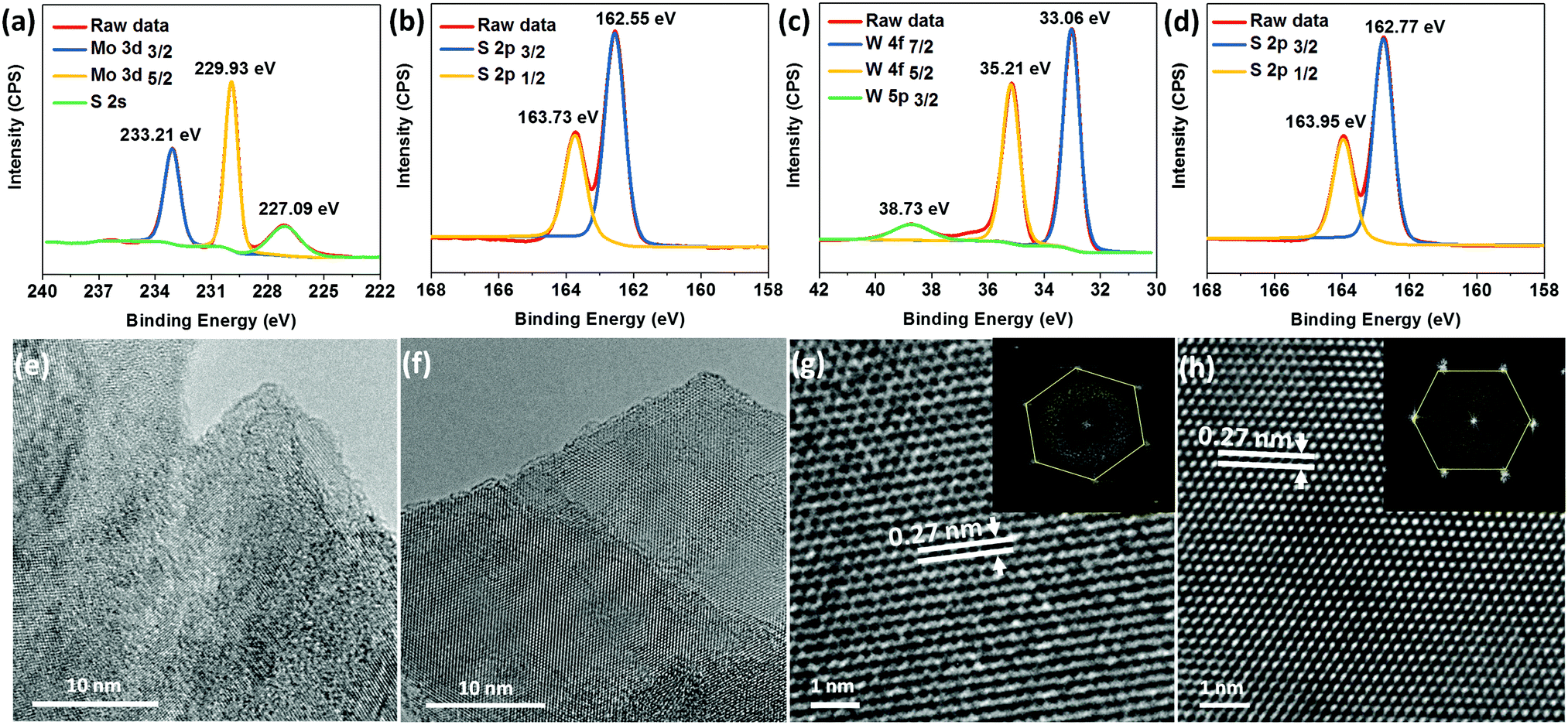 | ||
| Fig. 2 XPS spectra of the MoS2 and WS2 nanosheets deposited on ITO electrodes. (a) Mo3d, (b) S 2p, (c) W 4f, and (d) S 2p regions. TEM images of (e) MoS2 and (f) WS2 nanosheets. HRTEM images of (g) MoS2 and (h) WS2 with a d-spacing of 0.27 nm corresponding to the (100) plane. Inset: FFT patterns extracted from the HRTEM images, indicating the hexagonal symmetry. | ||
The structural properties of the exfoliated nanosheets were further investigated via HR-TEM. Fig. 2e–h show TEM images of the exfoliated TMD nanosheets. Evidently, the flakes consist of a few layers, which can be considered as an indication of efficient exfoliation. The HR-TEM (Fig. 2g and h) and fast Fourier transform (FFT) data analysis (inset Fig. 2g and h) for MoS2 and WS2 reveal the expected hexagonal symmetry and high structural quality of the nanosheets.12 The d-spacings of both MoS2 and WS2 were measured to be 0.27 nm, which corresponds to the (100) plane.32 These findings are in line with the Raman and AFM results.
The potential use of exfoliated MoS2 and WS2 as a hole transporting layer (HTL) was investigated in a ternary bulk-heterojunction (BHJ) layer consisting of the donor polymer PBDB-T-2F, the non-fullerene small-molecule acceptor (NFA) Y6, and the fullerene acceptor PC71BM (Fig. 3a).30,33,34 Poly[(9,9-bis(3′-((N,N-dimethyl)-N-ethylammonium)-propyl)-2,7-fluorene)-alt-2,7-(9,9-dioctylfluorene)]dibromide (PFN-Br) was used as the electron-transport layer (ETL), while spin-coated layers of the MoS2 and WS2 suspensions were used as the HTL. Measuring the actual thickness of the formed TMD layers deposited atop the ITO electrode proved difficult due the high roughness of the latter. The resulting device structure is shown in the inset of Fig. 3b. Reference cells utilizing poly(3,4-ethylene dioxythiophene):poly(styrenesulfonate) (PEDOT:PSS) as the HTL were also prepared for comparison.
 | ||
| Fig. 3 (a) Molecular structures of PBDB-T-2F, Y6 and PC71BM. (b) J–V curves of PBDB-T-2F:Y6:PC71BM based OSCs without a HTL (w/o) and with WS2, MoS2 and PEDOT:PSS as the HTL. Inset: Schematic of the cell architecture. (c) EQE spectra of the cells shown in (b). | ||
Fig. 3b shows the J–V curves of the various optimized solar cells, while Fig. S2 (ESI†) shows representative data for cells based on WS2 and MoS2 prepared at different centrifugation speeds. The OSCs with WS2 as the HTL exhibit higher performance than the MoS2-based cells, with a maximum PCE of 15.6%, open-circuit voltage (Voc) of 0.83 V, short-circuit current (Jsc) of 26.0 mA cm−2, and fill factor (FF) of 0.72%. On the other hand, the optimised MoS2-based OSCs exhibit a slightly lower PCE (14.9%), Voc (0.81 V), Jsc (25.3 mA cm−2), and FF (0.71). To further investigate the impact of different HTLs we extracted the series resistance (Rs) and shunt resistance (Rsh) from the J–V curves, which are summarized in Table 1. Evidently, the presence of WS2 and MoS2 reduces Rs from 3.9 Ω (bare ITO) to 3.2 Ω and 3.3 Ω, respectively. On the other hand, the use of WS2 and MoS2 increases the Rsh value from 630 Ω (bare ITO) to 1140 Ω and 991 Ω, respectively. Because of the reduced Rs and improved Rsh, the WS2 and MoS2-based OSCs exhibit enhanced FF and PCE.35,36 Importantly, the PCE values of both the WS2 and MoS2-based cells are significantly higher than the devices without any HTL, i.e. bare ITO (8.6%), and are comparable to that obtained for optimised OSCs based on a commercial PEDOT:PSS HTL (16.0%). Further refinement of the LPE process in tandem with improved device engineering is expected to lead to further device performance improvements.
| HTL | V oc [V] | J sc [mA cm−2] | J cal [mA cm−2] | FF | PCE [%] | R s [Ω] | R sh [Ω] |
|---|---|---|---|---|---|---|---|
| a Values of Jcal were obtained from the integrated EQE spectra. b Average values calculated from 10 devices. | |||||||
| WS2 | 0.83 (0.81 ± 0.1)b | 26.0 (25.5 ± 0.3)b | 25.3 | 0.72 (0.70 ± 0.2)b | 15.6 (15.2 ± 0.2)b | 3.2 | 1140 |
| MoS2 | 0.81 (0.79 ± 0.1)b | 25.3 (24.9 ± 0.2)b | 24.7 | 0.71 (0.68 ± 0.2)b | 14.9 (14.3 ± 0.4)b | 3.3 | 991 |
| PEDOT:PSS | 0.85 (0.84 ± 0.1)b | 25.8 (25.5 ± 0.2)b | 25.1 | 0.73 (0.70 ± 0.2)b | 16.0 (15.7 ± 0.2)b | 3.0 | 1048 |
| w/o | 0.56 (0.55 ± 0.1)b | 24.3 (24.0 ± 0.1)b | 23.9 | 0.63 (0.58 ± 0.4)b | 8.6 (8.3 ± 0.2)b | 3.9 | 630 |
Fig. 3c displays the external quantum efficiency (EQE) spectra for the PBDBT-2F:Y6:PC71BM cells made with the different HTLs. For all devices the integrated photocurrent density (Table 1) deduced from the EQE spectra matches well the values obtained from the J–V analysis (Fig. 3b) within ±4%. The WS2-based cells exhibit higher photoresponse in the range 348–446 nm and 666–843 nm. However, the lower photoresponse seen in the range 448–553 nm, when compared to the PEDOT:PSS-based cells, results in a slightly increased Jsc and PCE. The cells without a HTL (bare ITO) exhibit the lowest EQE in the spectral range 580–880 nm, indicating that WS2 and MoS2 flakes assist in extracting the photogenerated electrons in this range. We attribute this to the favourable energetics of the low-dimensional HTL layers with respect to ITO and the BHJ layer, although other effects on the BHJ morphology cannot be fully excluded at this moment.
In an effort to rationalize the different effects of WS2 and MoS2 nanosheets on the device performance, we performed UPS measurements on ITO/TMD by a transfer process. Fig. S3 (ESI†) shows the measured spectra while Table S2 (ESI†) summarizes the key results. Evidently, the presence of TMDs changes the work function (WF) of the ITO electrode as determined by the secondary electron cut-off from 4.7 to 5.1 eV for WS2 and 5.04 eV for MoS2. The favourable WF combined with the electron blocking character of the TMDs, for this particular photoactive layer (Fig. S4, ESI†), is believed to be the main feature responsible for the enhanced cell performance as compared to bare ITO devices.30,34 However, other important effects, such as the ITO surface coverage by the TMDs, may also play a role and cannot be excluded.34 To address this, the surface coverage of ITO by the MoS2 and WS2 flakes was investigated using energy-dispersive X-ray spectroscopy (EDS). Fig. S5 (ESI†) shows the elemental maps for the two materials. Evidently, the WS2 flakes provide a better coverage of ITO than MoS2, consequently leading to solar cells with higher Voc and PCE. Overall, our results highlight the potential of NH3(aq.)-based exfoliation processes for the preparation of high quality TMD HTLs that could one day be used as a replacement for the hygroscopic and acidic PEDOT:PSS in organic optoelectronics.32,37
Conclusions
In conclusion, we successfully demonstrated liquid-phase exfoliation of MoS2 and WS2 in aqueous ammonia as an environmentally friendly alternative to the more commonly used solvents. The method is simple and scalable as it does not rely on the use of any stabilizers or surfactants and yields high concentration (0.5–1 mg mL−1) TMD suspensions. The yield could potentially be improved further via tuning of processing parameters such as the sonication time and temperature. The extracted 2D nanosheets exhibit high structural and stoichiometric quality with a p-type character; a critical characteristic for practical electronic applications as carrier-selective interlayers. Indeed, when MoS2 and WS2 were used as HTLs, OSCs with a PCE up to 14.9% and 15.6%, respectively, were obtained. Our result highlights the potential of the NH3(aq.)-based LPE route for the preparation of high quality 2D TMD HTL materials.Experimental
Liquid exfoliation procedure
WS2 and MoS2 powders were purchased from Sigma Aldrich and NH3(aq.) was purchased from Alfa Aesar. We sonicated commercial WS2 (40 mg) and MoS2 (30 mg) powders in 10 mL of NH3(aq.) (50% v/v) using a horn probe sonic tip for 3 h (750 W, 20% amplitude). To avoid processing damage and minimize heating of the solution, the tip pulse was set as 5 s on and 2 s off. Also, sonication was carried out in a water bath cooling system to keep the temperature at 5 °C. After sonication, the obtained dispersions were transferred to centrifuge tubes and centrifuged at speeds differing from 3000 rpm to 8000 rpm to remove bulk aggregates. Then the supernatants on the top were carefully collected avoiding the extraction of precipitated bulk particles. Supernatants with colours ranging from dark brown to light yellow depending on the centrifugation speed were obtained. It is expected that at high centrifugation speeds thick and large sheets sediment, and supernatants consisting of thin and small nanosheets remain on the top. Due to the volatility of ammonia, the suspensions were kept at 5 °C as it was found to extend their shelf life to months.AFM characterization
For the AFM measurement, we spin-coated (1500 rpm) the prepared nanosheets from the suspensions onto Si/SiO2 substrates. The tapping mode of a Veeco AFM instrument from Bruker was used for all the measurements.XPS measurements
XPS measurements were performed at 0.5–1 × 10⁻⁹ mbar using an Omicron spectrometer with a monochromatic Al Kα X-ray Omicron XM1000 X-ray source (hν = 1486.6 eV). The operation power was set as 389 W. The high-resolution spectra and surveys were acquired at constant analyzer pass energies of 15 and 50 eV, respectively. The ambient contamination C1s (carbon, 284.7 eV) was used as a reference for the calibration of the binding energy and sample charging. Casa XPS software was used to analyse the spectra. The fitting of spectra was performed after Shirley-type background subtraction.TEM characterization
For the TEM characterization, MoS2 and WS2 nanosheets were drop-cast onto lacey carbon/Ni grids and used for TEM analysis. The imaging was performed using a TEM instrument of model Titan 80-300 ST from ThermoFisher Scientific.Solar cell fabrication
PBDB-T-2F, Y6, and PC71BM were purchased from Solarmer Materials Inc. Indium tin oxide (ITO) coated glass substrates (Kintec Company, 10 Ω sq.−1) were cleaned by sequential ultrasonication in dilute Extran 300 detergent solution, deionized water, acetone, and isopropyl alcohol for 10 min each. The substrates were then subjected to a UV-ozone treatment for 20 min. Next, a thin layer (≈30 nm) of PEDOT:PSS was spin-coated onto the UV-treated substrates and then dried on a heating plate at 150 °C for 10 min. For the HTL, the dispersion containing WS2 or MoS2 nanosheets was spin-coated at 1500 rpm for 60 s onto the UV-treated substrates. The samples were then transferred into a dry nitrogen glove box (<10 ppm O2). For PBDB-T-2F:Y6:PC71BM BHJs, a solution was prepared with ratio 1:1:0.2 with a concentration of 16 mg mL−1 in chloroform and added 0.5% (volume) chloronaphthalene. The solutions were then spun to obtain an active-layer thickness in the narrow range of 140–150 nm. A layer of 5 nm of PFN-Br as an ETL was spun from methanol solution (0.5 mg mL−1) on top of the BHJ layer. Finally, the samples were placed in a thermal evaporator and 100 nm of aluminum was then thermally evaporated at 5 × 10⁻⁶ mbar through a 0.1 cm2 pixel area shadow mask.
Conflicts of interest
There are no conflicts to declare.Acknowledgements
The authors acknowledge financial support from King Abdullah University of Science and Technology (KAUST). Part of this work was supported by the King Abdullah University of Science and Technology (KAUST) Office of Sponsored Research (OSR) under Award No: OSR-2018-CARF/CCF-3079.References
- Q. H. Wang, K. Kalantar-Zadeh, A. Kis, J. N. Coleman and M. S. Strano, Nat. Nanotechnol., 2012, 7, 699–712 CrossRef CAS PubMed.
- A. O’Neill, U. Khan and J. N. Coleman, Chem. Mater., 2012, 24, 2414–2421 CrossRef.
- X. Huang, Z. Zeng and H. Zhang, Chem. Soc. Rev., 2013, 42, 1934–1946 RSC.
- U. Halim, C. R. Zheng, Y. Chen, Z. Lin, S. Jiang, R. Cheng, Y. Huang and X. Duan, Nat. Commun., 2013, 4, 2213 CrossRef PubMed.
- V. Nicolosi, M. Chhowalla, M. G. Kanatzidis, M. S. Strano and J. N. Coleman, Science, 2013, 340, 1226419 CrossRef.
- N. Peimyoo, J. Shang, W. Yang, Y. Wang, C. Cong and T. Yu, Nano Res., 2014, 8, 1210–1221 CrossRef.
- E. P. Nguyen, B. J. Carey, T. Daeneke, J. Z. Ou, K. Latham, S. Zhuiykov and K. Kalantar-zadeh, Chem. Mater., 2014, 27, 53–59 CrossRef.
- H. S. Matte, A. Gomathi, A. K. Manna, D. J. Late, R. Datta, S. K. Pati and C. N. Rao, Angew. Chem., Int. Ed., 2010, 49, 4059–4062 CrossRef CAS PubMed.
- L. Niu, J. N. Coleman, H. Zhang, H. Shin, M. Chhowalla and Z. Zheng, Small, 2016, 12, 272–293 CrossRef CAS PubMed.
- G. L. Frey, K. J. Reynolds, R. H. Friend, H. Cohen and Y. Feldman, J. Am. Chem. Soc., 2003, 125, 5998–6007 CrossRef CAS PubMed.
- S. Luo, S. Dong, C. Lu, C. Yu, Y. Ou, L. Luo, J. Sun and J. Sun, J. Colloid Interface Sci., 2018, 513, 389–399 CrossRef CAS PubMed.
- K. Manna, H. N. Huang, W. T. Li, Y. H. Ho and W. H. Chiang, Chem. Mater., 2016, 28, 7586–7593 CrossRef CAS.
- C. Backes, T. M. Higgins, A. Kelly, C. Boland, A. Harvey, D. Hanlon and J. N. Coleman, Chem. Mater., 2016, 29, 243–255 CrossRef.
- G. S. Bang, K. W. Nam, J. Y. Kim, J. Shin, J. W. Choi and S. Y. Choi, ACS Appl. Mater. Interfaces, 2014, 6, 7084–7089 CrossRef CAS PubMed.
- J. Shen, Y. He, J. Wu, C. Gao, K. Keyshar, X. Zhang, Y. Yang, M. Ye, R. Vajtai, J. Lou and P. M. Ajayan, Nano Lett., 2015, 15, 5449–5454 CrossRef CAS PubMed.
- M. Wang, X. Xu, Y. Ge, P. Dong, R. Baines, P. M. Ajayan, M. Ye and J. Shen, ACS Appl. Mater. Interfaces, 2017, 9, 9168–9175 CrossRef CAS PubMed.
- J. Kim, S. Kwon, D. H. Cho, B. Kang, H. Kwon, Y. Kim, S. O. Park, G. Y. Jung, E. Shin, W. G. Kim, H. Lee, G. H. Ryu, M. Choi, T. H. Kim, J. Oh, S. Park, S. K. Kwak, S. W. Yoon, D. Byun, Z. Lee and C. Lee, Nat. Commun., 2015, 6, 8294 CrossRef CAS PubMed.
- N. B. Vargaftik, B. N. Volkov and L. D. Voljak, J. Phys. Chem. Ref. Data, 1983, 12, 817–820 CrossRef CAS.
- Z. Tahir, E. Alocilja and D. Grooms, Sensors, 2007, 7, 1123–1140 CrossRef CAS.
- R. Bari, D. Parviz, F. Khabaz, C. D. Klaassen, S. D. Metzler, M. J. Hansen, R. Khare and M. J. Green, Phys. Chem. Chem. Phys., 2015, 17, 9383–9393 RSC.
- K. Wang, J. Wang, J. Fan, M. Lotya, A. O'Neill, D. Fox, Y. Feng, X. Zhang, B. Jiang, Q. Zhao, H. Zhang, J. N. Coleman, L. Zhang and W. J. Blau, ACS Nano, 2013, 7, 9260–9267 CrossRef CAS PubMed.
- W. Zhao, Z. Ghorannevis, K. K. Amara, J. R. Pang, M. Toh, X. Zhang, C. Kloc, P. H. Tan and G. Eda, Nanoscale, 2013, 5, 9677–9683 RSC.
- N. Dong, Y. Li, Y. Feng, S. Zhang, X. Zhang, C. Chang, J. Fan, L. Zhang and J. Wang, Sci. Rep., 2015, 5, 14646 CrossRef CAS PubMed.
- K. F. Mak, C. Lee, J. Hone, J. Shan and T. F. Heinz, Phys. Rev. Lett., 2010, 105, 136805 CrossRef PubMed.
- W. Zhao, Z. Ghorannevis, L. Chu, M. Toh, C. Kloc, P. H. Tan and G. Eda, ACS Nano, 2013, 7, 791–797 CrossRef CAS PubMed.
- H. Zeng, G. B. Liu, J. Dai, Y. Yan, B. Zhu, R. He, L. Xie, S. Xu, X. Chen, W. Yao and X. Cui, Sci. Rep., 2013, 3, 1608 CrossRef PubMed.
- G. Pagona, C. Bittencourt, R. Arenal and N. Tagmatarchis, Chem. Commun., 2015, 51, 12950–12953 RSC.
- H. Liu, L. Xu, W. Liu, B. Zhou, Y. Zhu, L. Zhu and X. Jiang, J. Colloid Interface Sci., 2018, 515, 27–31 CrossRef CAS PubMed.
- L. Yin, X. Hai, K. Chang, F. Ichihara and J. Ye, Small, 2018, 14, 1704153 CrossRef PubMed.
- G. L. Frey, K. J. Reynolds and R. H. Friend, Adv. Mater., 2002, 14, 265–268 CrossRef CAS.
- H. Liu, N. Han and J. Zhao, RSC Adv., 2015, 5, 17572–17581 RSC.
- E. Singh, K. S. Kim, G. Y. Yeom and H. S. Nalwa, ACS Appl. Mater. Interfaces, 2017, 9, 3223–3245 CrossRef CAS PubMed.
- Z. Liu, S. P. Lau and F. Yan, Chem. Soc. Rev., 2015, 44, 5638–5679 RSC.
- Y. Lin, B. Adilbekova, Y. Firdaus, E. Yengel, H. Faber, M. Sajjad, X. Zheng, E. Yarali, A. Seitkhan, O. M. Bakr, A. El-Labban, U. Schwingenschlögl, V. Tung, I. McCulloch, F. Laquai and T. D. Anthopoulos, Adv. Mater., 2019, 31, 1902965 CrossRef CAS PubMed.
- H. Lian, N. Jun, A. Bolag, A. Hexig, N. Gerile, O. Tegus and S. Lin, Solid State Phenom., 2019, 288, 113–118 Search PubMed.
- Z. Zheng, Q. Hu, S. Zhang, D. Zhang, J. Wang, S. Xie, R. Wang, Y. Qin, W. Li, L. Hong, N. Liang, F. Liu, Y. Zhang, Z. Wei, Z. Tang, T. P. Russell, J. Hou and H. Zhou, Adv. Mater., 2018, 30, 1801801 CrossRef PubMed.
- X. Gu, W. Cui, H. Li, Z. Wu, Z. Zeng, S.-T. Lee, H. Zhang and B. Sun, Adv. Energy Mater., 2013, 3, 1262–1268 CrossRef CAS.
Footnote |
| † Electronic supplementary information (ESI) available: Experimental details, photovoltaic parameters of OSCs, EQE, UPS and PL data. See DOI: 10.1039/d0tc00659a |
| This journal is © The Royal Society of Chemistry 2020 |