
Double peak emission in lead halide perovskites by self-absorption†
Konstantin
Schötz
a,
Abdelrahman M.
Askar
 b,
Wei
Peng
c,
Dominik
Seeberger
d,
Tanaji P.
Gujar‡
d,
Mukundan
Thelakkat
d,
Anna
Köhler
ae,
Sven
Huettner
d,
Osman M.
Bakr
c,
Karthik
Shankar
b and
Fabian
Panzer
*a
b,
Wei
Peng
c,
Dominik
Seeberger
d,
Tanaji P.
Gujar‡
d,
Mukundan
Thelakkat
d,
Anna
Köhler
ae,
Sven
Huettner
d,
Osman M.
Bakr
c,
Karthik
Shankar
b and
Fabian
Panzer
*a
aSoft Matter Optoelectronics, University of Bayreuth, 95440 Bayreuth, Germany. E-mail: fabian.panzer@uni-bayreuth.de
bDepartment of Electrical and Computer Engineering, University of Alberta, Edmonton, AB T6G 1H9, Canada
cKing Abdullah University of Science and Technology (KAUST), Division of Physical Sciences and Engineering, Thuwal 23955-6900, Kingdom of Saudi Arabia
dDepartment of Chemistry, University of Bayreuth, 95440 Bayreuth, Germany
eBayreuth Institute of Macromolecular Research (BIMF) and Bavarian Polymer Institute (BPI), University of Bayreuth, 95440 Bayreuth, Germany
First published on 7th January 2020
Abstract
Despite the rapidly increasing efficiencies of perovskite solar cells, the optoelectronic properties of this material class are not completely understood. Especially when measured photoluminescence (PL) spectra consist of multiple peaks, their origin is still debated. In this work, we investigate in detail double peak PL spectra of halide perovskite thin films and single crystals with different material compositions. By different optical spectroscopic approaches and quantitative models, we demonstrate that the additional PL peak results from an extensive self-absorption effect, whose impact is intensified by strong internal reflections. This self-absorption accounts for the unusual temperature dependence of the additional PL peak and it implies that absorption until far into the perovskite's Urbach tail is important. The internal reflections entail that even for thin films self-absorption can have a significant contribution to the PL spectrum. Our results allow for a clear assignment of the PL peaks by differentiating between optical effects and electronic transitions, which is a necessary requirement for understanding the optoelectronic properties of halide perovskites.
1. Introduction
Halide perovskites, and optoelectronic devices based on them such as solar cells, LEDs, lasers or detectors, have undergone a tremendous development in the last few years. For this, their optical properties, in particular the absorption and photoluminescence (PL) spectra, play an important role when investigating the perovskite materials such as to derive conclusions about their electronic structure.1,2 For example, phase transitions and different structural states can be identified by the associated optical spectra, which are experimentally easily accessible. Furthermore, from the analysis of the spectra, important material parameters can be determined, such as electron phonon coupling constants or dynamic and static disorder (in particular by temperature-dependent investigations).3–8 PL signatures of different defect states both at higher and especially at lowest temperatures were identified,6,9,10 and the interaction of the perovskite with its environment (solvent, humidity or atmosphere) was investigated using PL measurements.11–13 More recently, spatially resolved PL investigations allowed to associate the occurrence of defect assisted, non-radiative decay channels with the grain boundaries of the perovskite.14 This has facilitated the development of appropriate passivation strategies, which in turn have led to the last significant increases in efficiencies of perovskite solar cells.15–17However, although PL spectroscopy has been used intensively and versatilely in the past, it is still common for PL spectra measured under nominally identical conditions to differ from work to work or from group to group, and in many cases to exhibit several peaks within a PL band. Hence, there is still an intense discussion and disagreement about the origin of these multiple PL features, and a variety of interpretations exists. Some suggest the additional PL features to stem from the coexistence of a direct and an indirect bandgap,18–22 defect induced recombination of (bound) excitons,21,23–25 different electronic structure between the bulk and the surface,26–28 coexistence of different crystalline phases10,29 and to self-absorption effects.30–33 Evidently, clarification on the origin of the multiple peak structure is urgently needed to allow for further understanding of the optoelectronic structure of lead halide perovskites.
In this work, we demonstrate that the occurrence of double peak structure is a general phenomenon in lead halide perovskites and not limited to single crystals or a specific material composition. We systematically address the different existing interpretations and show that neither the recombination via different types of defects, or different electronic states between the bulk and the surface can account for the double peak structure. Instead, from temperature dependent one-photon-induced and two-photon-induced PL measurements, optical modelling, and a systematic change of measurement geometry, we conclude that the additional PL feature is due to a surprisingly extensive self-absorption effect, significantly amplified by internal reflections of PL. Finally, we show that by changing the refractive index of the perovskite environment, and thus the internal reflectivity, the relative intensity of the two peaks can be modified, further underpinning our approach.
2. Results and discussion
2.1 The double-peak structure
Fig. 1a shows the room temperature photoluminescence (PL) of four different lead halide perovskites used in this study, namely a MAPbI3 thin film, a MAPbI3 single crystal, a single crystal with a different halide, MAPbBr3, and a single crystal with a different organic cation, EA0.17MA0.83PbI3. For all samples, we observe the emission to be structured, i.e. to consist of a dominant higher energy peak that we will refer to as “Peak 1” and of a weaker lower energy peak or shoulder, henceforth called “Peak 2”. This emission structure occurs independently of chemical composition and film structure for our four model samples, stressing the general nature of the phenomenon. The energy of the emission band varies with sample composition. For the iodide perovskites, Peak 1 is located at 1.56 eV in the case of the single crystals, and at 1.58 eV for the thin film. While for the single crystals, Peak 2 appears as distinct peak at 1.48 eV, in the case of the thin film Peak 2 is located at 1.53 eV, i.e. less separated from corresponding Peak 1 and it is thus observed as a shoulder. For clarity, an alternative version of Fig. 1a with a logarithmic PL scale can be found in the ESI† (Fig. S1). For MAPbBr3, Peak 1 and Peak 2 are located at 2.29 eV and 2.21 eV respectively. The relative PL intensity of Peak 2 compared to Peak 1 is in the range between 30 to 60% for all samples, depending on the position of excitation and detection spot and the angle of detection (see Fig. S2, ESI†).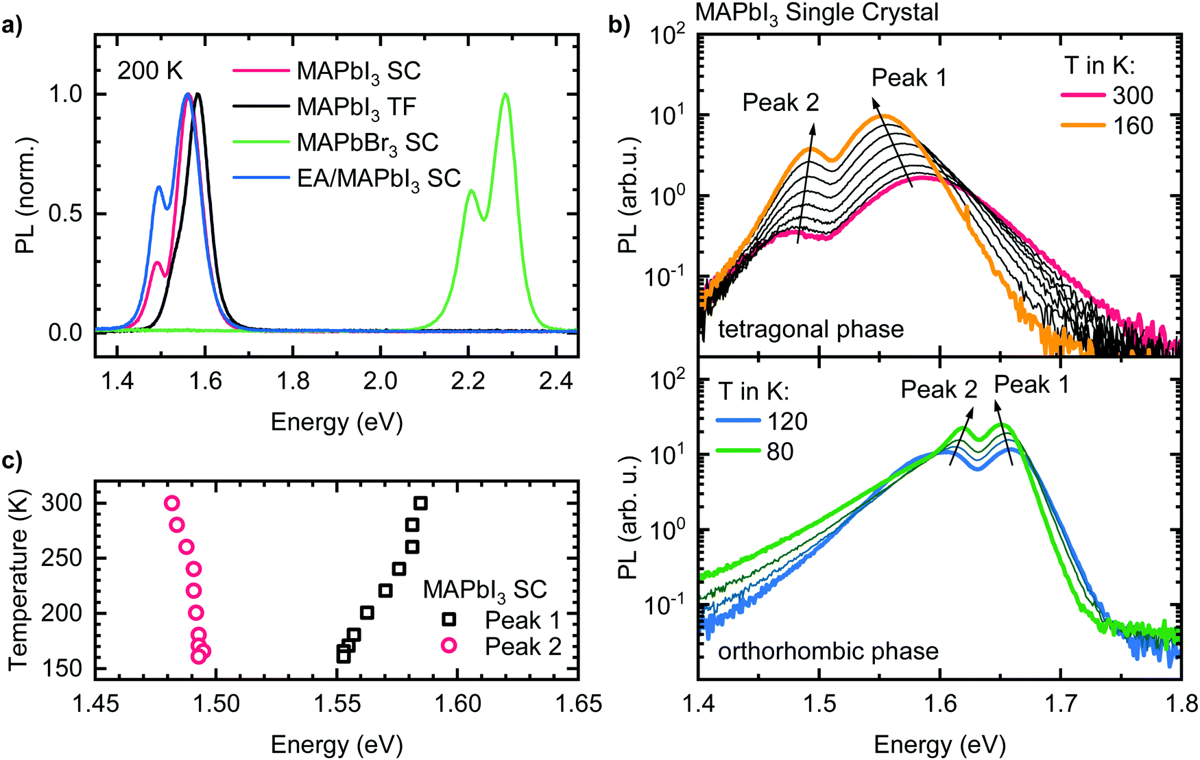 | ||
| Fig. 1 (a) Normalized PL spectra of four different lead halide perovskite samples showing double peak emission. (b) Temperature-dependent PL of a MAPbI3 single crystal between 300 K (red) and 160 K (orange), i.e. tetragonal phase in steps of 20 K (top) and in the orthorhombic phase between 120 K (blue) and 80 K (green). (c) Temperature-dependent peak position of Peak 1 and Peak 2 from the PL shown in (b) after spectral decomposition. | ||
To further investigate the two PL peaks, we performed temperature dependent PL measurements on all samples. Exemplarily, the results for the MAPbI3 single crystal are shown in Fig. 1b (see Fig. S3 (ESI†) for the results of the other compounds). Upon cooling from 300 K to 160 K (Fig. 1b), where MAPbI3 is in the tetragonal phase, the PL intensities of both peaks increase by an order of magnitude. Even without further analysis, it is evident that Peak 1 shifts to lower energies upon cooling, while the opposite is the case for Peak 2. Separating the spectra into the contributions of two individual peaks (see Fig. S4, ESI†) shows that Peak 1 shifts continuously to lower energies by 32 meV upon cooling, while Peak 2 shifts to higher energies by 10 meV until 240 K and then stays energetically constant (Fig. 1c).
Upon cooling below 160 K, MAPbI3 undergoes a phase transition from a tetragonal to an orthorhombic crystal structure,34 which is accompanied by an 100 meV increase of the band gap, directly impacting on the absorption and PL properties.35–37 Until 120 K a transition region exists in which the different phases coexist leading to PL spectra with more than two PL features (Fig. S5, ESI†). Between 120 K and 80 K we again observe two PL-Peaks, which exhibit the same spectral temperature dependence as Peak 1 and Peak 2 in the tetragonal phase (i.e. shift to lower (higher) energies of Peak 1 (Peak 2) with decreasing temperature). Below 80 K additional PL features appear, leading to relatively complex PL spectra at lowest temperatures (Fig. S6, ESI†). It becomes obvious that additional well-resolved/distinct PL bands can be observed over the entire investigated temperature range, i.e. also over different crystal phases.
2.2 Investigating possible structural origins for the double peak
Several interpretations have been proposed to account for the structure in the emission bands. We shall evaluate whether these interpretations are consistent with our data one by one.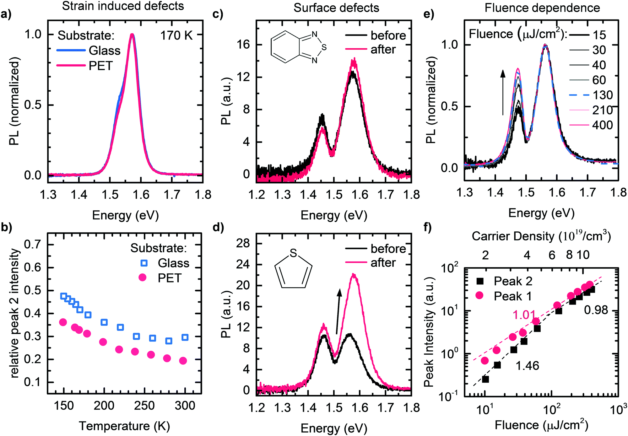 | ||
| Fig. 2 (a) PL of MAPbI3 thin films at 170 K processed on glass (blue) and on PET (red). (b) Temperature dependence of the PL Peak 2 intensity relative to Peak 1 intensity of the two thin films processed on glass (blue squares) and PET (red dots). (c and d) Room temperature PL of a MAPbI3 single crystal before (black) and after (red) surface passivation with (c) benzothiadiazole dissolved in cyclohexane and (d) mono-thiophene. (e) Fluence dependent PL (normalized) of a MAPbI3 single crystal at 200 K and (f) corresponding peak intensities as a function of laser fluence, plotted on a double logarithmic scale. The dashed lines represent fits with slope values as indicated. | ||
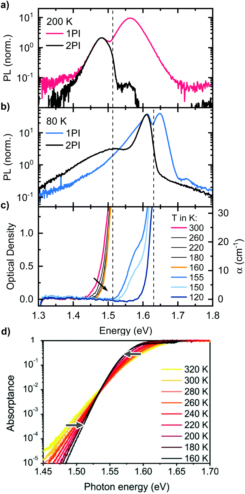 | ||
| Fig. 3 One-photon-induced (1PI) and two-photon-induced (2PI) PL of a MAPbI3 single crystal, (a) at 200 K (tetragonal phase) and (b) at 80 K (orthorhombic phase). (c) Optical density of a MAPbI3 single crystal in the temperature range from 300 K to 120 K. The arrow indicates reducing temperature. (d) Temperature-dependence of the Urbach-tail absorption. Reprinted with permission from Ledinsky et al.,74 Copyright 2019 American Chemical Society. | ||
2.3 Addressing optical effects as possible origin for the double-peak structure
So far, we could establish that Peak 2 results from the bulk while Peak 1 is associated with PL near the surface. We did not find any structural causes in the bulk that could account for Peak 2. We therefore consider whether self-absorption may be associated with the occurrence of the double peak structure. For this, it is obviously useful to consider the absorption of the perovskite crystals. Thus, we determined the temperature-dependent optical density of the MAPbI3 single crystal by transmission measurements (Fig. 3c). With our experimental setup, we can reliably determine optical densities (OD) in the range from about 0.1 to 1.5. This corresponds to absorption coefficients α in the range of 1 to 30 cm−1, considering a thickness of 1 mm, which is typical for the single crystals we used. Such low α-values occur in the Urbach tail of MAPbI3, which has been characterized in the past using photothermal deflection spectroscopy (PDS) or external quantum efficiency (EQE) measurements.70–72 At 300 K, detectable absorption for our setup starts at 1.44 eV and rises steeply to an OD of 1.5 at 1.5 eV. Importantly, upon cooling, the detectable absorption shifts to higher energies and the absorption edge becomes steeper. Below 160 K, the absorption jumps to 1.63 eV, indicating the transition to the orthorhombic phase.34,35 This is accompanied by an additional well-resolved shoulder at 1.58 eV that matches the energy for absorption of the tetragonal phase of thin films at this temperature.4,73 Evidently, some small residues of tetragonal phase still prevail at 155 K and 150 K. An estimation considering a crystal thickness of 1 mm and the absorption coefficient of MAPbI3 as reported by Crothers et al.70 implies that approximately 0.1% of tetragonal phase are still present at 155 K. The shift of the measured absorption of the single crystal to higher energies upon cooling from 300 K to 160 K is opposite to the trend observed for the absorption edge of thin films. However, it can be understood when considering which part of the absorption spectrum we probe with our transmission measurement: both the estimated values of the absorption coefficient and the energetic position of the absorption edge indicate that we measure Urbach tail absorption below the so called Urbach focus point, which was found for MAPbI3 to be around 1.54 eV, where the absorption coefficient takes a value of α = 500 cm−1.60,74 For absorption coefficients below this point, the temperature-dependence of the absorption is inversed, i.e. the absorption edge shifts to higher energies upon cooling, in accordance with our results. For clarification, the temperature-dependence of the Urbach-tail, including the Urbach focus point, is displayed in Fig. 3d, taken from Ledinsky et al.74 The arrows indicate the temperature-evolution above and below the Urbach focus point. We also would like to emphasize that the measured absorption edge of the single crystal only represents a small part of the Urbach tail and cannot be used to determine the optical band gap of the material and thus does not imply a red shifted band gap of the single crystal compared to thin films.The temperature dependent absorption spectra reveal two important facts: first, significant absorption, which reduces the transmission of photons generated deep in the crystal bulk to less than 10%, occurs in the same energetic range as the high energy edge of the 2PI-PL, both for the tetragonal (1.51 eV) and the orthorhombic phase (1.63 eV) as indicated by dashed lines in Fig. 3. This is essentially the position of the minimum between Peak 1 and 2. A similar observation was reported for MAPbBr3 single crystals by Yamada et al. comparing transmission with 2PI-PL measurements.33 Second, the shift of the absorption to higher energies upon cooling from 300 K to 160 K, matches well with the temperature dependence of the energetic position of Peak 2 in Fig. 1c. These two observations are a strong indication that the occurrence of Peak 2 is correlated to a self-absorption effect.
To test the plausibility of self-absorption as origin of Peak 2, we modelled our 1PI-PL by explicitly considering the effect that self-absorption will have on emission generated throughout the crystal as illustrated in Fig. 4. To do so, we calculated the one-dimensional charge carrier distribution n(x) that results from laser excitation. For this, we considered the absorption coefficient of MAPbI3 at 337 nm, which can be found e.g. in Crothers et al.,70 and the Beer–Lambert-law. This charge carrier distribution leads to photoluminescence via bimolecular recombination. The PL generated by recombination at a site x′ can then travel towards either to front or the backside of the crystal, which are taken to be 1 mm apart. This is about the size of the single crystals examined in this study. On the way through the crystal, the perovskite absorbs part of the PL, thus attenuating it. At the interface between perovskite and surrounding media, the PL is either transmitted or reflected with a certain probability. A key feature of our model is that we allow for multiple inner reflections. The PL that is detected at the front surface is then a superposition of the PL that leaves the crystal at the front without internal reflections, PLdirect(E), and the PL that leaves the crystal after (multiple) internal reflections, PLfiltered(E).
| PLdetected(E) = C·PLdirect(E) + PLfiltered(E). | (1) |
 | (2) |
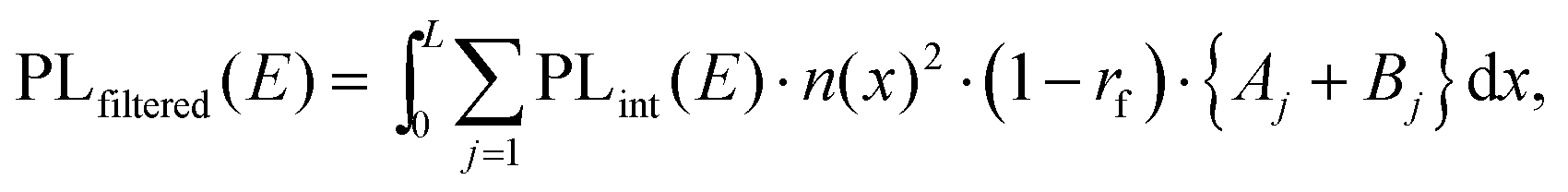 | (3) |
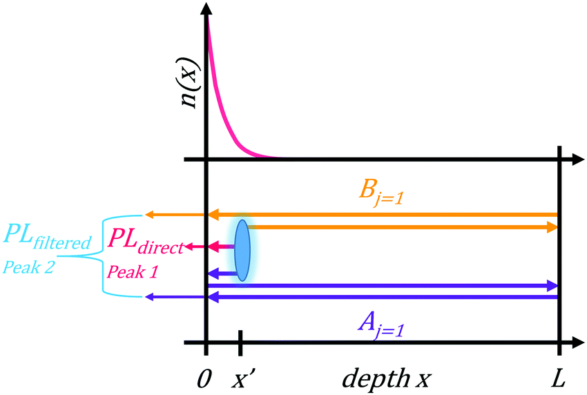 | ||
| Fig. 4 Illustration of the optical paths considered in the optical modeling. From a certain depth in the crystal x′, the PL can either hit the front surface and escape with a certain probability (red), contributing to Peak 1 (PLdirect), or can be reflected and travel towards the back surface. There it is reflected with a certain probability and travels back to the front surface, where it is either transmitted (purple) and contributes to Peak 2 (PLfiltered), or reflected again. Alternatively, the PL originating from x′ can travel to the back, being reflected and traveling to the front, where it likewise can either escape (orange), contributing to Peak 2, or be reflected. On its way through the crystal, the PL is filtered by the absorption of the perovskite. | ||
The comparison between the PL spectrum calculated using our model (with a value of C = 0.66) and the experimental PL spectrum of the MAPbI3 single crystal at room temperature is shown by the black squares and the black line in Fig. 5a. The excellent agreement for this simple model – which only uses a single “fitting” factor in the form of C – clearly demonstrates the significant importance of self-absorption. Fig. 5b indicates which part of the PL results from the directly transmitted PL, PLdirect(E), and from PL that suffered internal reflections and self-absorption, PLfiltered(E). We stress again here the key role of considering multiple reflections. Effects that are neglected in our model are carrier diffusion, photon recycling and internal scattering. Carrier diffusion and photon recycling both have similar effects insofar that they can generate PL at a site that is different from the original absorption. While photon recycling can have significant impact on the PL properties76,77 and should, together with carrier diffusion, enhance the intensity of Peak 2, we found it was not necessary to include photon recycling explicitly to model our measured spectra.
To further test whether self-absorption, magnified by reflection at the crystal back surface, is indeed causing the double peak structure, we repeated the room temperature 1PI-PL of the same MAPbI3 single crystal while modifying the outcoupling, and thus the reflection, at the back surface. For this, we placed a drop of glycerin at the backside of the crystal, while we excited the sample and detected resulting PL at the front side, identical to the previous measurement. This measurement was performed directly after the one without glycerin drop without moving the crystal or detection, to exclude any influence of a changed measurement geometry. The refractive index of glycerin is 1.47,78i.e. higher than the one of air, which reduces the reflection probability at the backside of the crystal from 0.85 to 0.70. According to our model, this should lead to a decreased intensity of Peak 2, accompanied by a spectral shift to higher energies. The obtained experimental data and the model data (keeping all parameters identical to before, except of the reflection probability), are shown as red line and dots in Fig. 5a. We find the intensity of Peak 2 to reduce to half the previous value and to shift to the blue by 10 meV. This observation is excellently captured by our model.
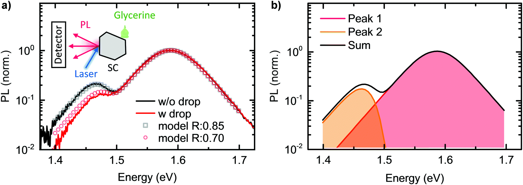 | ||
| Fig. 5 (a) PL spectrum of a MAPbI3 single crystal in air at room temperature (black solid line) together with the modelled PL with an internal reflection probability of 0.85 (black open squares). The PL spectrum of the same crystal with a drop of glycerin at the back is displayed as red solid line, together with the modeled PL with an internal reflection probability at the back interface of 0.7 (red open circles). (b) Decomposition of the modelled PL into the contribution of the PL coming directly from the excitation spot (PLdirect, Peak 1, red) and the PL after internal reflections and self-absorption (PLfiltered, Peak 2, orange). | ||
These findings represent compelling evidence that Peak 2 originates from an extreme self-absorption effect, which is caused by significant internal reflections in the temperature ranges investigated in this study. We stress that below about 80 K, the temperature-dependence of Peak 2 changes, probably due to an increasing contribution of PL of bound exciton states,79 which becomes increasingly efficient at lower temperatures. In passing we mention that changes in reflectivity for example due to the addition of thiophene or benzothiadiazole, or due to different substrates such as Glass and PET can easily account for the slightly different intensities of Peak 2 that we observed in Fig. 2a and b.
With the insight provided by our results on the different origin of Peak 1 and 2, we can understand the different temperature dependence of Peak 1 and 2 in their PL spectra, with Peak 1 shifting to the red spectral range and Peak 2 to the blue upon cooling. Peak 1, resulting from PLdirect(E), is modified by reabsorption only from the point where it was created, to the front surface. Reabsorption thus occurs over a typical lengthscale of about 50 nm, depending on the wavelength of excitation. A significant attenuation, say, to a level of 10% of transmitted intensity, would be then obtained for absorption coefficients above about of 5 × 105 cm−1. If diffusion of charge carriers is considered, the lengthscale increases to the μm range, and the relevant absorption coefficient decreases to about 104 cm−1. In contrast, reabsorption for Peak 2 occurs over a length scale exceeding the crystal thickness of 1 mm, thus becoming relevant for absorption coefficients as low as a few 10 cm−1. Fig. 3d, taken from Ledinsky et al., shows the evolution of the Urbach tail with temperature.74 The two arrows indicate the typical absorption coefficients associated with self-absorption for PLdirect(E), which causes Peak 1, and for PLfiltered(E) that gives rise to Peak 2. One can see that the two ranges for the absorption are on different sides of the Urbach focus point. As a result, cooling causes a blue-shift for Peak 2 due to filter effects, despite Peak 1 shifting to the red due to the decreasing bandgap of the perovskite.
In the framework of filtered PL which we present here, also the dependence of the relative intensity of Peak 2 from the excitation spot and/or the detection angle can be understood easily. Due to the high refractive index of the perovskite, the direct PL is limited to its escape cone at the spot where the PL is generated. In contrast, the filtered PL can travel large distances and thus can also leave the crystal far away from the excitation spot or at the side surfaces of the crystal. This is in agreement with a very recent study by Kojima et al., where the authors demonstrate by angle dependent PL of a MAPbBr3 crystal, that direct PL is limited to a small escape cone, whereas filtered PL is also detected from the side and the backside of the crystal.80
If we apply our model to fit the PL of the MAPbI3 thin film from Fig. 1a, it turns out that we need to set the sample thickness to 3.5 μm to model the experimental data satisfyingly. However, the actual thickness of the sample is 0.7 μm, indicating that our model is over-simplified for the application for thin films. This points towards the importance to also consider the lateral component of the propagation direction of the light.
We finally note that the long optical pathways in halide perovskites can also impact their photocurrent measurements. For excitation in the spectral range of the Urbach tail, penetration lengths can be on the length scale of mm, so that the entire sample volume is excited and contributes to charge carrier generation. This can overcompensate the higher density of generated charges for excitation at higher photon energies, where the absorption coefficient is bigger, but the penetration length is limited to tens of nanometers. A peak of the photocurrent in the spectral region of the Urbach tail would be the consequence, bearing danger of misinterpretation if optical effects are not considered.
3. Conclusion
In summary, we have shown that the often observed double peak PL spectra of halide perovskites result from a significant self-absorption effect, which is amplified by the high internal reflection probability of PL in the sample, with Peak 1 being the emission directly outcoupled, and Peak 2 being emission that suffered multiple internal reflections and pronounced self-absorption. This effect not only impacts on the spectra of single crystals but also occurs in thin film spectra, and it is not limited to a specific perovskite composition, thus rendering it a general phenomenon. We found absorption from the Urbach-tail of the perovskite to be highly relevant for the self-absorption-effect, because optical paths in the sample can easily be on the length scale of millimeters. By controlled reduction of the reflection probability at the back side of a single crystal we could experimentally alter the intensity of the additional PL peak, thus providing compelling evidence for our conclusion. Using a relatively simple quantitative model, we were also able to simulate the PL spectra including the additional peaks and the spectral shifts that were observed in the experiment upon changing the reflectivity. Our results will help to interpret photoluminescence spectra of lead halide perovskites correctly by delivering a better understanding of the effects and importance of self-absorption and internal reflections in this material class.4. Experimental section
4.1 Sample preparation
MAPbI3 single crystals were prepared following the inverse temperature crystallization technique.81 In brief, the synthesis started with a 1–1.3 M solution of MAI (from Dyesol-Limited, Now GreatCell Solar) and PbI2 (Sigma-Aldrich) in gamma-butyrolactone (GBL, Sigma-Aldrich). The precursors dissolved in GBL after 30 minutes of vigorous stirring at 60 °C. Upon filtering the solution using 0.22 μm PVDF filters, the stock solution was then distributed into small vials with 3–4 ml of solution each. The vials were kept undisturbed in an oil bath for 3–4 hours at 110 °C. Once the desired size of the crystals was achieved, the crystals were removed from the synthesis solution, washed quickly with fresh GBL, dried with a N2 flow.EA0.17MA0.83PbI3 single crystals were grown using the antisolvent-vapor diffusion assisted crystallization method, as reported elsewhere.82,83 In brief, the precursor solutions were prepared by dissolving proper amount of methylammonium iodide, ethylammonium iodide and PbI2 in γ-butyrolactone in a ratio of 0.15 M![[thin space (1/6-em)]](https://www.rsc.org/images/entities/char_2009.gif) :0.15 M:0.1 M. The precursor solutions were then loaded in a small crystallizing dish with aluminum foil cover, which was then placed in a bigger dish with antisolvent, namely dichloromethane, loaded. The whole setup was sealed with an aluminum foil cover. The inner cover was left with a ∼0.5 mm hole to let the antisolvent vapor diffuse inside the precursor solution. The growth process usually takes 4–6 days.
:0.15 M:0.1 M. The precursor solutions were then loaded in a small crystallizing dish with aluminum foil cover, which was then placed in a bigger dish with antisolvent, namely dichloromethane, loaded. The whole setup was sealed with an aluminum foil cover. The inner cover was left with a ∼0.5 mm hole to let the antisolvent vapor diffuse inside the precursor solution. The growth process usually takes 4–6 days.
For the Synthesis of the MAPbBr3 single crystals, a 1 M solution of MAPbBr3 in DMF was prepared by mixing equimolar amounts of MABr and PbBr2 in DMF over a period of 1 h. 5–10 ml of the solution were filtered over a 200 nm PTFE filter and placed in a glass Petri dish. The Petri dish was placed on a hotplate and set to 47.5 °C. The heat was increased slowly until the first nuclei were forming outside the mould. Then the temperature was increased to 75 °C with a rate of 5 °C per hour. The crystals were removed from the hot solution and washed with ether.
For fabrication of the MAPbI3 thin films, the substrates were cleaned with detergent followed by sonication in deionized water, acetone and ethanol for 10 min each, and dried with clean dry air. After ozone treatment (at 50° for 15 min with 2 l per min O3 flow), the substrates were transferred in a glovebox under N2 atmosphere. For MAPbI3 formation, we adapted a published procedure84,85 and optimized it as follows. PbI2 (1 M) was dissolved in N,N-dimethyl formamide overnight under stirring conditions at 100 °C and 80 μl solution was spin coated on the quartz substrates at 2000 rpm for 50 s, and dried at 100 °C for 5 min. 100 mg MAI powder (see ESI† for details) was spread out around the PbI2 coated substrates with a Petri dish covering on the top and heated at 165 °C for 13 h for full conversion.
4.2 Photoluminescence and absorption measurements
The temperature-dependent 1PI-PL of all samples and the fluence-dependent PL were performed using a home-build setup. The samples were put in a continuous flow cryostat (Oxford Instruments, Optistat CF) connected to a temperature controller (Oxford Instruments ITC503S). The sample is excited with a 337 nm nitrogen laser (LTB MNL 100). The signal is collected via a charge-coupled device (CCD) camera (Andor iDus DU420a-OE) coupled to a spectrograph (Andor Shamrock SR303i).The passivation experiments and the experiments with the glycerin drop at the back of the crystal were performed on air at room temperature. The crystals were excited using the nitrogen laser (LTB MNL 100) and the emitted PL was collected with an optical fiber and detected by a CCD camera (Andor iDus DU420A-OE) coupled to a spectrograph (LOT Oriel MS125). For both measurements, the sample was not moved between initial and final measurement. For the passivation measurement, it was ensured that all liquid evaporated before the final PL measurement by waiting for five minutes.
For temperature-dependent 2PI-PL measurements, the perovskite crystals used for this experiment were placed in a continuous flow cryostat, connected to a temperature controller (Oxford Instruments MercuryITC). For excitation, we used a mode-locked titanium-sapphire laser (Coherent Chameleon Ultra), with its emission center wavelength adjusted to 1000 nm. The laser power was reduced to 26 mW at 4.73 MHz and focused to a spot with a beam waist of 0.01 mm at the position of the sample. For the transmission measurements of the single crystal, a broadly fluorescent material was placed in the cryostat and its PL was measured once without and once with crystal in front of it. This technique has the advantage against conventional transmission measurements that diffraction effects that deflect the transmitted light from the optical axis play only a little role.
For each set of experiments, a new crystal was used to exclude any influence of degradation effects by previous measurements on the results of the experiment. All PL data were corrected by the corresponding setup efficiency.
Author contributions
FP initiated, and planned the project. KoS performed all optical characterizations and derived the optical model. FP, AK and KoS discussed the project. AMA synthesized the MAPbI3 single crystals under supervision of KaS. WP synthesized the EAMAPbI3 single crystals under supervision of OMB. DS synthesized the MAPbBr3 single crystals under supervision of SH. TG produced the MAPbI3 thin films under the supervision of MT. FP and KoS wrote the manuscript which was revised by all authors. FP supervised the project.Conflicts of interest
There are no conflicts to declare.Acknowledgements
KoS acknowledges financial support from the German National Science Foundation (Project KO 3973/2-1 and GRK 1640). AK, SH and MT acknowledges support by the Bavarian State Ministry of Science, Research, and the Arts for the Collaborative Research Network ‘‘Solar Technologies go Hybrid’’. KaS acknowledges financial support from NSERC (grant number 06630) and NRC (grant number A1-014009). WP and OMB acknowledge the financial support of KAUST. Furthermore, we thank Daniel Niesner and Laura Herz for fruitful discussions, and Yu Zhong for the help with film characterizations.References
- L. M. Herz, Charge-Carrier Dynamics in Organic–Inorganic Metal Halide Perovskites, Annu. Rev. Phys. Chem., 2016, 67, 65–89 CrossRef CAS PubMed.
- Y. Kanemitsu, Luminescence Spectroscopy of Lead-Halide Perovskites: Materials Properties and Application as Photovoltaic Devices, J. Mater. Chem. C, 2017, 5(14), 3427–3437 RSC.
- T. Meier, T. P. Gujar, A. Schönleber, S. Olthof, K. Meerholz, S. van Smaalen, F. Panzer, M. Thelakkat and A. Köhler, Impact of Excess PbI2 on the Structure and the Temperature Dependent Optical Properties of Methylammonium Lead Iodide Perovskites, J. Mater. Chem. C, 2018, 6(28), 7512–7519 RSC.
- F. Panzer, C. Li, T. Meier, A. Köhler and S. Huettner, Impact of Structural Dynamics on the Optical Properties of Methylammonium Lead Iodide Perovskites, Adv. Energy Mater., 2017, 7(16), 1700286 CrossRef.
- A. D. Wright, C. Verdi, R. L. Milot, G. E. Eperon, M. A. Perez-Osorio, H. J. Snaith, F. Giustino, M. B. Johnston and L. M. Herz, Electron-Phonon Coupling in Hybrid Lead Halide Perovskites, Nat. Commun., 2016, 7, 11755 CrossRef PubMed.
- R. L. Milot, G. E. Eperon, H. J. Snaith, M. B. Johnston and L. M. Herz, Temperature-Dependent Charge-Carrier Dynamics in CH3NH3PbI3 Perovskite Thin Films, Adv. Funct. Mater., 2015, 25(39), 6218–6227 CrossRef CAS.
- C. Wehrenfennig, M. Z. Liu, H. J. Snaith, M. B. Johnston and L. M. Herz, Homogeneous Emission Line Broadening in the Organo Lead Halide Perovskite CH3NH3PbI3-xClx, J. Phys. Chem. Lett., 2014, 5(8), 1300–1306 CrossRef CAS PubMed.
- F. Panzer, S. Baderschneider, T. P. Gujar, T. Unger, S. Bagnich, M. Jakoby, H. Bässler, S. Huettner, J. Köhler, R. Moos, M. Thelakkat, R. Hildner and A. Köhler, Reversible Laser Induced Amplified Spontaneous Emission from Coexisting Tetragonal and Orthorhombic Phases in Hybrid Lead Halide Perovskites, Adv. Opt. Mater., 2016, 4(6), 917–928 CrossRef CAS.
- X. X. Wu, M. T. Trinh, D. Niesner, H. M. Zhu, Z. Norman, J. S. Owen, O. Yaffe, B. J. Kudisch and X. Y. Zhu, Trap States in Lead Iodide Perovskites, J. Am. Chem. Soc., 2015, 137(5), 2089–2096 CrossRef CAS PubMed.
- C. Wehrenfennig, M. Z. Liu, H. J. Snaith, M. B. Johnston and L. M. Herz, Charge Carrier Recombination Channels in the Low-Temperature Phase of Organic-Inorganic Lead Halide Perovskite Thin Films, APL Mater., 2014, 2(8), 081513 CrossRef.
- J. Li, A. Dobrovolsky, A. Merdasa, E. L. Unger and I. G. Scheblykin, Luminescent Intermediates and Humidity-Dependent Room-Temperature Conversion of the MAPbI3 Perovskite Precursor, ACS Omega, 2018, 3(10), 14494–14502 CrossRef CAS PubMed.
- Y. Tian, M. Peter, E. Unger, M. Abdellah, K. Zheng, T. Pullerits, A. Yartsev, V. Sundstrom and I. G. Scheblykin, Mechanistic Insights into Perovskite Photoluminescence Enhancement: Light Curing with Oxygen can Boost Yield Thousandfold, Phys. Chem. Chem. Phys., 2015, 17(38), 24978–24987 RSC.
- G. Grancini, V. D'Innocenzo, E. R. Dohner, N. Martino, A. R. S. Kandada, E. Mosconi, F. De Angelis, H. I. Karunadasa, E. T. Hoke and A. Petrozza, CH3NH3PbI3 Perovskite Single Crystals: Surface Photophysics and their Interaction with the Environment, Chem. Sci., 2015, 6(12), 7305–7310 RSC.
- D. W. deQuilettes, S. M. Vorpahl, S. D. Stranks, H. Nagaoka, G. E. Eperon, M. E. Ziffer, H. J. Snaith and D. S. Ginger, Impact of Microstructure on Local Carrier Lifetime in Perovskite Solar Cells, Science, 2015, 348(6235), 683–686 CrossRef CAS PubMed.
- Q. Jiang, Y. Zhao, X. Zhang, X. Yang, Y. Chen, Z. Chu, Q. Ye, X. Li, Z. Yin and J. You, Surface Passivation of Perovskite Film for Efficient Solar Cells, Nat. Photonics, 2019, 13(7), 460–466 CrossRef CAS.
- N. K. Noel, A. Abate, S. D. Stranks, E. S. Parrott, V. M. Burlakov, A. Goriely and H. J. Snaith, Enhanced Photoluminescence and Solar Cell Performance via Lewis Base Passivation of Organic Inorganic Lead Halide Perovskites, ACS Nano, 2014, 8(10), 9815–9821 CrossRef CAS PubMed.
- M. Abdi-Jalebi, Z. Andaji-Garmaroudi, S. Cacovich, C. Stavrakas, B. Philippe, J. M. Richter, M. Alsari, E. P. Booker, E. M. Hutter, A. J. Pearson, S. Lilliu, T. J. Savenije, H. Rensmo, G. Divitini, C. Ducati, R. H. Friend and S. D. Stranks, Maximizing and Stabilizing Luminescence from Halide Perovskites with Potassium Passivation, Nature, 2018, 555(7697), 497–501 CrossRef CAS PubMed.
- E. M. Hutter, M. C. Gélvez-Rueda, A. Osherov, V. Bulović, F. C. Grozema, S. D. Stranks and T. J. Savenije, Direct-Indirect Character of the Bandgap in Methylammonium Lead Iodide Perovskite, Nat. Mater., 2017, 16(1), 115–120 CrossRef CAS PubMed.
- T. Wang, B. Daiber, J. M. Frost, S. A. Mann, E. C. Garnett, A. Walsh and B. Ehrler, Indirect to Direct Bandgap Transition in Methylammonium Lead Halide Perovskite, Energy Environ. Sci., 2017, 10(2), 509–515 RSC.
- B. Wu, H. F. Yuan, Q. Xu, J. A. Steele, D. Giovanni, P. Puech, J. H. Fu, Y. F. Ng, N. F. Jamaludin, A. Solanki, S. Mhaisalkar, N. Mathews, M. B. J. Roeffaers, M. Grätzel, J. Hofkens and T. C. Sum, Indirect Tail States Formation by Thermal-Induced Polar Fluctuations in Halide Perovskites, Nat. Commun., 2019, 10, 484 CrossRef PubMed.
- J. H. Fu, N. F. Jamaludin, B. Wu, M. J. Li, A. Solanki, Y. F. Ng, S. Mhaisalkar, C. H. A. Huan and T. C. Sum, Localized Traps Limited Recombination in Lead Bromide Perovskites, Adv. Energy Mater., 2019, 9(12), 1803119 CrossRef.
- J. A. Steele, P. Puech, B. Monserrat, B. Wu, R. X. Yang, T. Kirchartz, H. Yuan, G. Fleury, D. Giovanni, E. Fron, M. Keshavarz, E. Debroye, G. Zhou, T. C. Sum, A. Walsh, J. Hofkens and M. B. J. Roeffaers, Role of Electron–Phonon Coupling in the Thermal Evolution of Bulk Rashba-Like Spin-Split Lead Halide Perovskites Exhibiting Dual-Band Photoluminescence, ACS Energy Lett., 2019, 2205–2212 CrossRef CAS.
- X. Chi, K. Leng, B. Wu, D. Shi, Y. Choy, Z. Chen, Z. Chen, X. Yu, P. Yang, Q.-H. Xu, T. C. Sum, A. Rusydi and K. P. Loh, Elucidating Surface and Bulk Emission in 3D Hybrid Organic-Inorganic Lead Bromide Perovskites, Adv. Opt. Mater., 2018, 6(15), 1800470 CrossRef.
- J. Shi, H. Zhang, Y. Li, J. J. Jasieniak, Y. Li, H. Wu, Y. Luo, D. Li and Q. Meng, Identification of High-Temperature Exciton States and their Phase-Dependent Trapping Behaviour in Lead Halide Perovskites, Energy Environ. Sci., 2018, 11(6), 1460–1469 RSC.
- D. Niesner, O. Schuster, M. Wilhelm, I. Levchuk, A. Osvet, S. Shrestha, M. Batentschuk, C. Brabec and T. Fauster, Temperature-Dependent Optical Spectra of Single-Crystal (CH3NH3) PbBr3 Cleaved in Ultrahigh Vacuum, Phys. Rev. B, 2017, 95(7), 075207 CrossRef.
- B. Murali, S. Dey, A. L. Abdelhady, W. Peng, E. Alarousu, A. R. Kirmani, N. C. Cho, S. P. Sarmah, M. R. Parida, M. I. Saidaminov, A. A. Zhumekenov, J. Y. Sun, M. S. Alias, E. Yengel, B. S. Ooi, A. Amassian, O. M. Bakr and O. F. Mohammed, Surface Restructuring of Hybrid Perovskite Crystals, ACS Energy Lett., 2016, 1(6), 1119–1126 CrossRef CAS.
- B. Murali, E. Yengel, C. Yang, W. Peng, E. Alarousu, O. M. Bakr and O. F. Mohammed, The Surface of Hybrid Perovskite Crystals: A Boon or Bane, ACS Energy Lett., 2017, 2(4), 846–856 CrossRef CAS.
- S. T. Birkhold, E. Zimmermann, T. Kollek, D. Wurmbrand, S. Polarz and L. Schmidt-Mende, Impact of Crystal Surface on Photoexcited States in Organic-Inorganic Perovskites, Adv. Funct. Mater., 2017, 27(6), 1604995 CrossRef.
- F. Chen, C. Zhu, C. X. Xu, P. Fan, F. F. Qin, A. G. Manohari, J. F. Lu, Z. L. Shi, Q. Y. Xu and A. L. Pan, Crystal Structure and Electron Transition Underlying Photoluminescence of Methylammonium Lead Bromide Perovskites, J. Mater. Chem. C, 2017, 5(31), 7739–7745 RSC.
- L. M. Pazos-Outón, M. Szumilo, R. Lamboll, J. M. Richter, M. Crespo-Quesada, M. Abdi-Jalebi, H. J. Beeson, M. Vrucinic, M. Alsari, H. J. Snaith, B. Ehrler, R. H. Friend and F. Deschler, Photon Recycling in Lead Iodide Perovskite Solar Cells, Science, 2016, 351(6280), 1430–1433 CrossRef PubMed.
- Y. Fang, H. Wei, Q. Dong and J. Huang, Quantification of Re-Absorption and Re-Emission Processes to Determine Photon Recycling Efficiency in Perovskite Single Crystals, Nat. Commun., 2017, 8, 14417 CrossRef CAS PubMed.
- Y. Yamada, T. Yamada, L. Q. Phuong, N. Maruyama, H. Nishimura, A. Wakamiya, Y. Murata and Y. Kanemitsu, Dynamic Optical Properties of CH3NH3Pbl3 Single Crystals as Revealed by One- and Two-Photon Excited Photoluminescence Measurements, J. Am. Chem. Soc., 2015, 137(33), 10456–10459 CrossRef CAS PubMed.
- T. Yamada, Y. Yamada, H. Nishimura, Y. Nakaike, A. Wakamiya, Y. Murata and Y. Kanemitsu, Fast Free-Carrier Diffusion in CH3NH3PbBr3 Single Crystals Revealed by Time-Resolved One- and Two-Photon Excitation Photoluminescence Spectroscopy, Adv. Electron. Mater., 2016, 2(3), 1500290 CrossRef.
- A. Poglitsch and D. Weber, Dynamic Disorder in Methylammoniumtrihalogenoplumbates(II) Observed by Millimeter-Wave Spectroscopy, J. Chem. Phys., 1987, 87(11), 6373–6378 CrossRef CAS.
- T. Ishihara, Optical-Properties of PbI-Based Perovskite Structures, J. Lumin., 1994, 60–61, 269–274 CrossRef CAS.
- W. G. Kong, Z. Y. Ye, Z. Qi, B. P. Zhang, M. Wang, A. Rahimi-Iman and H. Z. Wu, Characterization of an Abnormal Photoluminescence Behavior upon Crystal-Phase Transition of Perovskite CH3NH3PbI3, Phys. Chem. Chem. Phys., 2015, 17(25), 16405–16411 RSC.
- E. S. Parrott, R. L. Milot, T. Stergiopoulos, H. J. Snaith, M. B. Johnston and L. M. Herz, Effect of Structural Phase Transition on Charge-Carrier Lifetimes and Defects in CH3NH3SnI3 Perovskite, J. Phys. Chem. Lett., 2016, 7(7), 1321–1326 CrossRef CAS PubMed.
- D. Niesner, M. Wilhelm, I. Levchuk, A. Osvet, S. Shrestha, M. Batentschuk, C. Brabec and T. Fauster, Giant Rashba Splitting in CH3NH3PbBr3 Organic-Inorganic Perovskite, Phys. Rev. Lett., 2016, 117(12), 126401 CrossRef PubMed.
- D. Niesner, M. Hauck, S. Shrestha, I. Levchuk, G. J. Matt, A. Osvet, M. Batentschuk, C. Brabec, H. B. Weber and T. Fauster, Structural Fluctuations Cause Spin-Split States in Tetragonal CH3NH3PbI3 as Evidenced by the Circular Photogalvanic Effect, Proc. Natl. Acad. Sci. U. S. A., 2018, 115(38), 9509–9514 CrossRef CAS PubMed.
- S. D. Stranks and P. Plochocka, The Influence of the Rashba Effect, Nat. Mater., 2018, 17(5), 381–382 CrossRef CAS PubMed.
- L. Leppert, S. E. Reyes-Lillo and J. B. Neaton, Electric Field- and Strain-Induced Rashba Effect in Hybrid Halide Perovskites, J. Phys. Chem. Lett., 2016, 7(18), 3683–3689 CrossRef CAS PubMed.
- J. M. Richter, K. Chen, A. Sadhanala, J. Butkus, J. P. H. Rivett, R. H. Friend, B. Monserrat, J. M. Hodgkiss and F. Deschler, Direct Bandgap Behavior in Rashba-Type Metal Halide Perovskites, Adv. Mater., 2018, 30(52), e1803379 CrossRef PubMed.
- F. Zheng, L. Z. Tan, S. Liu and A. M. Rappe, Rashba Spin-Orbit Coupling Enhanced Carrier Lifetime in CH3NH3Pbl3, Nano Lett., 2015, 15(12), 7794–7800 CrossRef CAS PubMed.
- T. Etienne, E. Mosconi and F. De Angelis, Dynamical Origin of the Rashba Effect in Organohalide Lead Perovskites: A Key to Suppressed Carrier Recombination in Perovskite Solar Cells?, J. Phys. Chem. Lett., 2016, 7(9), 1638–1645 CrossRef CAS PubMed.
- M. Kepenekian and J. Even, Rashba and Dresselhaus Couplings in Halide Perovskites: Accomplishments and Opportunities for Spintronics and Spin-Orbitronics, J. Phys. Chem. Lett., 2017, 8(14), 3362–3370 CrossRef CAS PubMed.
- T. Kirchartz and U. Rau, Decreasing Radiative Recombination Coefficients via an Indirect Band Gap in Lead Halide Perovskites, J. Phys. Chem. Lett., 2017, 8(6), 1265–1271 CrossRef CAS PubMed.
- D. A. Egger, A. Bera, D. Cahen, G. Hodes, T. Kirchartz, L. Kronik, R. Lovrincic, A. M. Rappe, D. R. Reichman and O. Yaffe, What Remains Unexplained about the Properties of Halide Perovskites?, Adv. Mater., 2018, 30(20), e1800691 CrossRef PubMed.
- K. Frohna, T. Deshpande, J. Harter, W. Peng, B. A. Barker, J. B. Neaton, S. G. Louie, O. M. Bakr, D. Hsieh and M. Bernardi, Inversion Symmetry and Bulk Rashba Effect in Methylammonium Lead Iodide Perovskite Single Crystals, Nat. Commun., 2018, 9, 1829 CrossRef PubMed.
- C. L. Davies, M. R. Filip, J. B. Patel, T. W. Crothers, C. Verdi, A. D. Wright, R. L. Milot, F. Giustino, M. B. Johnston and L. M. Herz, Bimolecular Recombination in Methylammonium Lead Triiodide Perovskite is an Inverse Absorption Process, Nat. Commun., 2018, 9(1), 293 CrossRef PubMed.
- P. Azarhoosh, S. McKechnie, J. M. Frost, A. Walsh and M. van Schilfgaarde, Research Update: Relativistic Origin of Slow Electron-Hole Recombination in Hybrid Halide Perovskite Solar Cells, APL Mater., 2016, 4(9), 091501 CrossRef.
- W. Du, S. A. Ghetmiri, B. R. Conley, A. Mosleh, A. Nazzal, R. A. Soref, G. Sun, J. Tolle, J. Margetis, H. A. Naseem and S.-Q. Yu, Competition of Optical Transitions Between Direct and Indirect Bandgaps in Ge1−xSnx, Appl. Phys. Lett., 2014, 105(5), 051104 CrossRef.
- S. Al-Kabi, S. Ghetmiri, J. Margetis, W. Du, A. Mosleh, M. Alher, W. Dou, J. Grant, G. Sun, R. Soref, J. Tolle, B. Li, M. Mortazavi, H. Naseem and S. Q. Yu, Optical Characterization of Si-Based Ge1−xSnx Alloys with Sn Compositions up to 12%, J. Electron. Mater., 2016, 45(4), 2133–2141 CrossRef CAS.
- D. Stange, S. Wirths, N. von den Driesch, G. Mussler, T. Stoica, Z. Ikonic, J. M. Hartmann, S. Mantl, D. Grützmacher and D. Buca, Optical Transitions in Direct-Bandgap Ge1–xSnx Alloys, ACS Photonics, 2015, 2(11), 1539–1545 CrossRef CAS.
- S. Wirths, R. Geiger, N. von den Driesch, G. Mussler, T. Stoica, S. Mantl, Z. Ikonic, M. Luysberg, S. Chiussi, J. M. Hartmann, H. Sigg, J. Faist, D. Buca and D. Grutzmacher, Lasing in Direct-Bandgap GeSn Alloy Grown on Si, Nat. Photonics, 2015, 9(2), 88–92 CrossRef CAS.
- T. W. Jones, A. Osherov, M. Alsari, M. Sponseller, B. C. Duck, Y. K. Jung, C. Settens, F. Niroui, R. Brenes, C. V. Stan, Y. Li, M. Abdi-Jalebi, N. Tamura, J. E. Macdonald, M. Burghammer, R. H. Friend, V. Bulovic, A. Walsh, G. J. Wilson, S. Lilliu and S. D. Stranks, Lattice Strain Causes Non-Radiative Losses in Halide Perovskites, Energy Environ. Sci., 2019, 12(2), 596–606 RSC.
- X. Y. Li, Y. Q. Luo, M. V. Holt, Z. H. Cai and D. P. Fenning, Residual Nanoscale Strain in Cesium Lead Bromide Perovskite Reduces Stability and Shifts Local Luminescence, Chem. Mater., 2019, 31(8), 2778–2785 CrossRef CAS.
- Goodfellow GmbH, Datasheet polyethylene terephthalate (Polyester, PET, PETP); available from http://goodfellow.com/E/Polyethylene-terephthalate.html, last accessed September 3, 2019.
- Polymerdatabase, Datasheet poly(ethylene terephthalate) (PET), available from http://polymerdatabase.com/Commercial%20Polymers/PET.html, last accessed September 3, 2019.
- H. A. Schaeffer and R. Langfeld, Werkstoff Glas, Springer Vieweg, Berlin, Heidelberg, Germany, 2014, p. 46 Search PubMed.
- S. Singh, C. Li, F. Panzer, K. L. Narasimhan, A. Graeser, T. P. Gujar, A. Köhler, M. Thelakkat, S. Huettner and D. Kabra, Effect of Thermal and Structural Disorder on the Electronic Structure of Hybrid Perovskite Semiconductor CH3NH3PbI3, J. Phys. Chem. Lett., 2016, 7(15), 3014–3021 CrossRef CAS PubMed.
- T. J. Jacobsson, L. J. Schwan, M. Ottosson, A. Hagfeldt and T. Edvinsson, Determination of Thermal Expansion Coefficients and Locating the Temperature-Induced Phase Transition in Methylammonium Lead Perovskites Using X-ray Diffraction, Inorg. Chem., 2015, 54(22), 10678–10685 CrossRef CAS PubMed.
- J. Zhao, Y. Deng, H. Wei, X. Zheng, Z. Yu, Y. Shao, J. E. Shield and J. Huang, Strained Hybrid Perovskite Thin Films and Their Impact on the Intrinsic Stability of Perovskite Solar Cells, Sci. Adv., 2017, 3(11), eaao5616 CrossRef PubMed.
- A. Osherov, E. M. Hutter, K. Galkowski, R. Brenes, D. K. Maude, R. J. Nicholas, P. Plochocka, V. Bulovic, T. J. Savenije and S. D. Stranks, The Impact of Phase Retention on the Structural and Optoelectronic Properties of Metal Halide Perovskites, Adv. Mater., 2016, 28(48), 10757–10763 CrossRef CAS PubMed.
- F. Panzer, H. Bässler and A. Köhler, Temperature Induced Order-Disorder Transition in Solutions of Conjugated Polymers Probed by Optical Spectroscopy, J. Phys. Chem. Lett., 2017, 8(1), 114–125 CrossRef CAS PubMed.
- X. P. Zheng, B. Chen, J. Dai, Y. J. Fang, Y. Bai, Y. Z. Lin, H. T. Wei, X. C. Zeng and J. S. Huang, Defect Passivation in Hybrid Perovskite Solar Cells Using Quaternary Ammonium Halide Anions and Cations, Nat. Energy, 2017, 2(7), 17102 CrossRef CAS.
- S. P. Sarmah, V. M. Burlakov, E. Yengel, B. Murali, E. Alarousu, A. M. El-Zohry, C. Yang, M. S. Alias, A. A. Zhumekenov, M. I. Saidaminov, N. Cho, N. Wehbe, S. Mitra, I. Ajia, S. Dey, A. E. Mansour, M. Abdelsamie, A. Amassian, I. S. Roqan, B. S. Ooi, A. Goriely, O. M. Bakr and O. F. Mohammed, Double Charged Surface Layers in Lead Halide Perovskite Crystals, Nano Lett., 2017, 17(3), 2021–2027 CrossRef CAS PubMed.
- R. W. Boyd, Nonlinear Optics, Academic Press, Burlington, USA, 3rd edn, 2008, pp. 549–559 Search PubMed.
- M. Göppert-Mayer, Über Elementarakte mit zwei Quantensprüngen, Ann. Phys., 1931, 401(3), 273–294 CrossRef.
- G. Nagamine, J. O. Rocha, L. G. Bonato, A. F. Nogueira, Z. Zaharieva, A. A. R. Watt, C. H. de Brito Cruz and L. A. Padilha, Two-Photon Absorption and Two-Photon-Induced Gain in Perovskite Quantum Dots, J. Phys. Chem. Lett., 2018, 9(12), 3478–3484 CrossRef CAS PubMed.
- T. W. Crothers, R. L. Milot, J. B. Patel, E. S. Parrott, J. Schlipf, P. Müller-Buschbaum, M. B. Johnston and L. M. Herz, Photon Reabsorption Masks Intrinsic Bimolecular Charge-Carrier Recombination in CH3NH3PbI3 Perovskite, Nano Lett., 2017, 17(9), 5782–5789 CrossRef CAS PubMed.
- S. De Wolf, J. Holovsky, S. J. Moon, P. Loper, B. Niesen, M. Ledinsky, F. J. Haug, J. H. Yum and C. Ballif, Organometallic Halide Perovskites: Sharp Optical Absorption Edge and Its Relation to Photovoltaic Performance, J. Phys. Chem. Lett., 2014, 5(6), 1035–1039 CrossRef CAS PubMed.
- A. Sadhanala, F. Deschler, T. H. Thomas, S. E. Dutton, K. C. Goedel, F. C. Hanusch, M. L. Lai, U. Steiner, T. Bein, P. Docampo, D. Cahen and R. H. Friend, Preparation of Single-Phase Films of CH3NH3Pb(I1-x,Br-x)3 with Sharp Optical Band Edges, J. Phys. Chem. Lett., 2014, 5(15), 2501–2505 CrossRef CAS PubMed.
- V. D'Innocenzo, G. Grancini, M. J. Alcocer, A. R. Kandada, S. D. Stranks, M. M. Lee, G. Lanzani, H. J. Snaith and A. Petrozza, Excitons Versus Free Charges in Organo-Lead Tri-Halide Perovskites, Nat. Commun., 2014, 5, 3586 CrossRef PubMed.
- M. Ledinsky, T. Schönfeldová, J. Holovský, E. Aydin, Z. Hájková, L. Landová, N. Neyková, A. Fejfar and S. De Wolf, Temperature Dependence of the Urbach Energy in Lead Iodide Perovskites, J. Phys. Chem. Lett., 2019, 10(6), 1368–1373 CrossRef CAS PubMed.
- L. J. Phillips, A. M. Rashed, R. E. Treharne, J. Kay, P. Yates, I. Z. Mitrovic, A. Weerakkody, S. Hall and K. Durose, Dispersion Relation Data for Methylammonium Lead Triiodide Perovskite Deposited on a (100) Silicon Wafer Using a Two-Step Vapour-Phase Reaction Process, Data Brief, 2015, 5, 926–928 CrossRef PubMed.
- R. Brenes, M. Laitz, J. Jean, D. W. de Quilettes and V. Bulovic, Benefit from Photon Recycling at the Maximum-Power Point of State-of-the-Art Perovskite Solar Cells, Phys. Rev. Appl., 2019, 12(1), 014017 CrossRef CAS.
- I. Dursun, Y. Z. Zheng, T. L. Guo, M. De Bastiani, B. Turedi, L. Sinatra, M. A. Hague, B. Sun, A. A. Zhumekenov, M. I. Saidaminov, F. P. G. de Arquer, E. H. Sargent, T. Wu, Y. N. Gartstein, O. M. Bakr, O. F. Mohammed and A. V. Malko, Efficient Photon Recycling and Radiation Trapping in Cesium Lead Halide Perovskite Waveguides, ACS Energy Lett., 2018, 3(7), 1492–1498 CrossRef CAS.
- J. Rheims, J. Koser and T. Wriedt, Refractive-Index Measurements in the Near-IR Using an Abbe Refractometer, Meas. Sci. Technol., 1997, 8(6), 601–605 CrossRef CAS.
- L. Q. Phuong, Y. Nakaike, A. Wakamiya and Y. Kanemitsu, Free Excitons and Exciton-Phonon Coupling in CH3NH3PbI3 Single Crystals Revealed by Photocurrent and Photoluminescence Measurements at Low Temperatures, J. Phys. Chem. Lett., 2016, 7(23), 4905–4910 CrossRef CAS PubMed.
- K. Kojima, K. Ikemura, K. Matsumori, Y. Yamada, Y. Kanemitsu and S. F. Chichibu, Internal Quantum Efficiency of Radiation in a Bulk CH3NH3PbBr3 Perovskite Crystal Quantified by Using the Omnidirectional Photoluminescence Spectroscopy, APL Mater., 2019, 7(7), 071116 CrossRef.
- M. I. Saidaminov, A. L. Abdelhady, B. Murali, E. Alarousu, V. M. Burlakov, W. Peng, I. Dursun, L. F. Wang, Y. He, G. Maculan, A. Goriely, T. Wu, O. F. Mohammed and O. M. Bakr, High-Quality Bulk Hybrid Perovskite Single Crystals Within Minutes by Inverse Temperature Crystallization, Nat. Commun., 2015, 6, 7586 CrossRef PubMed.
- W. Peng, X. H. Miao, V. Adinolfi, E. Alarousu, O. El Tall, A. H. Emwas, C. Zhao, G. Walters, J. K. Liu, O. Ouellette, J. Pan, B. Murali, E. H. Sargent, O. F. Mohammed and O. M. Bakr, Engineering of CH3NH3PbI3 Perovskite Crystals by Alloying Large Organic Cations for Enhanced Thermal Stability and Transport Properties, Angew. Chem., Int. Ed., 2016, 55(36), 10686–10690 CrossRef CAS PubMed.
- D. Shi, V. Adinolfi, R. Comin, M. J. Yuan, E. Alarousu, A. Buin, Y. Chen, S. Hoogland, A. Rothenberger, K. Katsiev, Y. Losovyj, X. Zhang, P. A. Dowben, O. F. Mohammed, E. H. Sargent and O. M. Bakr, Low Trap-State Density and Long Carrier Diffusion in Organolead Trihalide Perovskite Single Crystals, Science, 2015, 347(6221), 519–522 CrossRef CAS PubMed.
- T. P. Gujar and M. Thelakkat, Highly Reproducible and Efficient Perovskite Solar Cells with Extraordinary Stability from Robust CH3NH3PbI3: Towards Large-Area Devices, Energy Technol., 2016, 4(3), 449–457 CrossRef CAS.
- F. Panzer, S. Baderschneider, T. P. Gujar, T. Unger, S. Bagnich, M. Jakoby, H. Bässler, S. Huettner, J. Köhler, R. Moos, M. Thelakkat, R. Hildner and A. Köhler, Reversible Laser-Induced Amplified Spontaneous Emission from Coexisting Tetragonal and Orthorhombic Phases in Hybrid Lead Halide Perovskites, Adv. Opt. Mater., 2016, 4(6), 917–928 CrossRef CAS.
Footnotes |
| † Electronic supplementary information (ESI) available. See DOI: 10.1039/c9tc06251c |
| ‡ Current address: Shardabai Pawar Mahila College, Shardanagar, Baramati, Pune-413115 (MS), India. |
| This journal is © The Royal Society of Chemistry 2020 |