Solution processed red organic light-emitting-diodes using an N-annulated perylene diimide fluorophore†
Received
11th October 2019
, Accepted 5th January 2020
First published on 8th January 2020
1. Introduction
Organic light-emitting diodes (OLEDs) have successfully been deployed in light fixtures, mobile phones, and televisions over the past few years owing to continued improvements in both performance and lifetimes.1–5 OLEDs are multilayer devices with each layer having a distinct function including charge-injection, charge-transport, and light emission. The active emissive layer (EML) dictates the colour and maximum efficiency of OLEDs. For solution processing of electronically active layers; spin-coating,6 roll-to-roll coating7 and inkjet printing8 are the most common methods used. Solution processing is more challenging than thermal evaporation due to difficulties in forming distinct layers one on top of each other without bleeding or swelling. In support of solution processing it has been demonstrated that solution processed OLEDs can match the performance of thermally evaporated OLEDs.9 To create high-performance solution-processed OLEDs both conjugated polymers10 and small molecules11 have been used as the core component of the EML.
To date, the efficiency and purity of red colour solution processed OLEDs remains behind that of other coloured OLEDs (i.e. blue, green and orange).12 This is primarily a result of low-energy fluorescence being competitive with non-radiative decay pathways.13 Most high efficient red-emitting materials are organometallic in nature14 and suffer from high costs and poor environmental stability. The design of new metal-free organic small molecules is a viable route towards low-cost, high-performance, large area red OLEDs.15
The perylene diimide (PDI) chromophore is an excellent building block for which to construct new emitters for solution-processed red OLEDs owing to a pure red colour, high quantum yield photoluminescence, and high thermal and photochemical stability.16–18 Furthermore, PDIs can be rendered soluble in a range of both polar and non-polar solvents and thus are suitable for large area roll-to-roll coating.19–21 PDI-based materials have found wide utility as active materials in transistors,22,23 solar cells24,25 and OLEDs.26–28 PDI-based OLEDs typically have pure deep red electroluminescence with the emission wavelength of 690 nm and CIE coordinates of (x = 0.69, y = 0.29).26 For example, stable red emission from a PDI-based OLED with an external quantum efficiency of 4.93% has been demonstrated.29
Here, we report red OLEDs based on an emissive dimeric PDI, namely tPDI2N-EH. This compound is an N-annulated PDI dimer that has found utility as a non-fullerene acceptor for organic photovoltaics.30 Blending tPDI2N-EH with polyfluorene based polymers and used as the EML lead to good-performance OLED devices. The optical and electrophysical properties of PFO:tPDI2N-EH blended films were studied. The best PFO:tPDI2N-EH blend OLEDs were compared with standard OLEDs based on PFO:F8BT blend films (F8BT = poly[(9,9-di-n-octylfluorenyl-2,7-diyl)-alt-(benzo[2,1,3]thiadiazol-4,8-diyl)]). Best devices were fabricated by slot-die coating, a roll-to-roll compatible method, as proof-of-concept.
2. Results and discussion
2.1 Materials selection
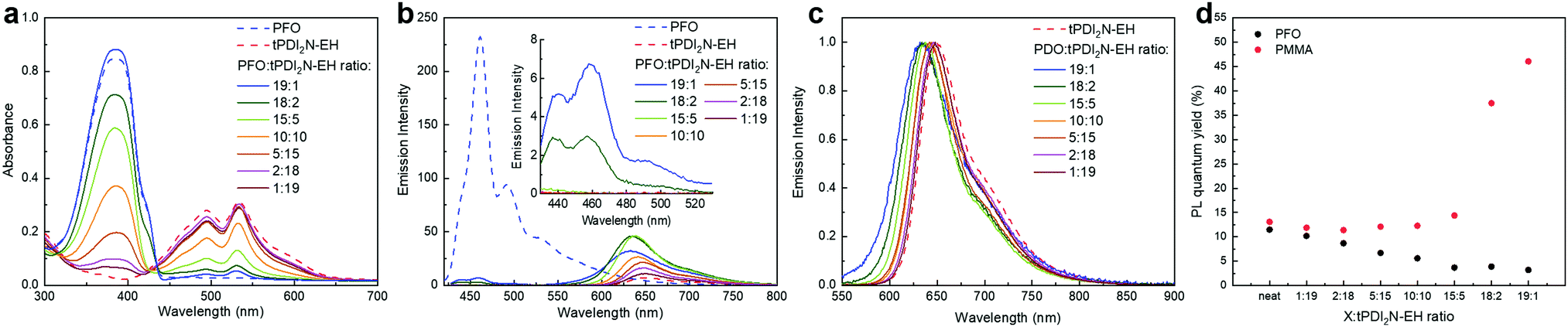
The N-annulated PDI dimer, tPDI2N-EH (Fig. 1a),30 can be synthesized on multi-gram scale, is semiconducting, and can be coated via roll-to-roll processes from non-halogenated solvents.19,20 It has a red luminescence peak at 650 nm (Fig. 1b) and is chemically stable as a film in sunlight. Thus, this material is appropriate for use as a solution processable light emitter. The luminescent conjugated polymers PFO and F8BT (structures are shown in Fig. 1a) were selected as a hole transporter and control emitter, respectively, since they exhibit high light stability31 and consistent performance as light emitters in OLEDs.32–35 A recent report has shown that PFO:F8BT-ink formulations are suitable to be slot-die coated into an OLED structure.36 PFO:F8BT based OLEDs were fabricated as control devices. The PFO polymer is p-type with appropriate electronic energy levels to pair with the F8BT or tPDI2N-EH to facilitate hole transport (Fig. 1c). Moreover, the wavelengths of the tPDI2N-EH absorption and PFO luminescence overlap (Fig. 1b and Fig. S1, ESI†) enabling Förster Resonance Energy Transfer (FRET) to occur from PFO to tPDI2N-EH. This makes the PFO:tPDI2N-EH system an excellent candidate as a OLED EML.
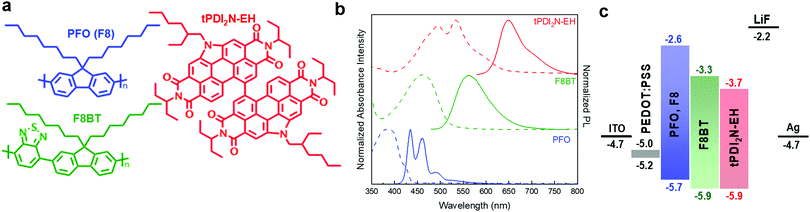 |
| | Fig. 1 (a) Chemical structures of the polymers PFO (F8) and F8BT, and the small molecule tPDI2N-EH used in this study. (b) Normalized absorption and photoluminescence spectra of PFO (blue dash and solid line), F8BT (green dash and solid line), and tPDI2N-EH (red dash and solid line) films spin-cast from toluene at 15 mg mL−1 under λex = 350 nm, 400 nm and 530 nm, respectively. (c) Energy level diagram with values for organic materials (energy levels taken from the relevant literature, the PEDOT:PSS has a work function of 5.0–5.2 eV). | |
2.2 OLEDs – spin-coated devices
Device fabrication and characterization.
OLED devices with the structure of glass/ITO/PEDOT:PSS/EML/LiF/Ag were fabricated and tested under ambient conditions. Control devices with an EML of PFO![[thin space (1/6-em)]](https://www.rsc.org/images/entities/char_2009.gif) :F8BT-blend film were spin-cast from toluene with the ratio of 19:1 at 15 mg mL−1. EMLs comprised of PFO:tPDI2N-EH-blend films were spin-cast from toluene at different ratios (from 19:1 to 1:19). The full details of the fabrication technique can be found in the ESI.† Electrical characterization of the devices was performed with a Keithley 2612B source-meter combined with the calibrated Si-photodiode and spectrometer.
:F8BT-blend film were spin-cast from toluene with the ratio of 19:1 at 15 mg mL−1. EMLs comprised of PFO:tPDI2N-EH-blend films were spin-cast from toluene at different ratios (from 19:1 to 1:19). The full details of the fabrication technique can be found in the ESI.† Electrical characterization of the devices was performed with a Keithley 2612B source-meter combined with the calibrated Si-photodiode and spectrometer.
OLED devices.
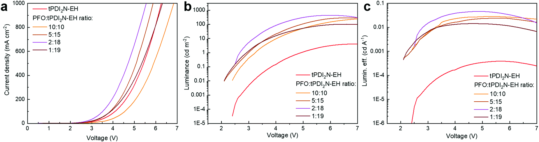
OLED device characteristics based on tPDI2N-EH and PFO:tPDI2N-EH-blend films with different ratios are shown in Fig. 3 and Table 2; the data include graphics of current density–voltage curves (J–V, Fig. 3a), luminance versus applied voltage curves (L–V, Fig. 3b) and luminous efficiency versus current density curves (LE–J, Fig. 3c). The OLEDs based on only tPDI2N-EH films as the EML showed a maximum luminous efficiency (LE) of around 4 × 10⁻³ cd A−1 with a maximum brightness of 4.1 cd m−2, which agree well with the previously obtained data for other PDI-based OLEDs.26 The highest performance OLEDs were based on PFO:tPDI2N-EH EML with the blend ratio of 2:18 and had the maximum LE of 0.05 cd A−1, power efficiency (PE) of 0.03 lm W−1, and external quantum efficiency (EQE) of 0.06%. Increasing the concentration of PFO in PFO:tPDI2N-EH-blend leads to performance deterioration of the fabricated OLEDs, which agrees well with the PL data (Fig. S2, ESI†). The turn-on voltage of the tPDI2N-EH-based OLEDs decreases when PFO is added to the EML. Adding the PFO, which has a higher lying HOMO energy level than tPDI2N-EH, helps facilitate hole injection from PEDOT:PSS to the EML. The turn-on voltage of 2.6 V for the OLEDs with PFO:tPDI2N-EH EMLs is the lowest reported for PDI-based OLEDs.26,27,29,38
 |
| | Fig. 3 (a) Current density–voltage (J–V) characteristics, (b) luminance versus applied voltage (L–V, cdm−2) and (c) luminous efficiency (lumin. eff.) versus current density (LE–J, cd A−1) of PFO:tPDI2N-EH OLEDs at selected ratios. | |
Table 2 Summary of device performance for OLEDs based on tPDI2N-EH and PFO:tPDI2N-EH-blend films with different ratio spin-coated on the glass
| Emitting layer |
Ratioa |
V
on
[V] |
EQEmaxc [%] |
LEmaxd [cd A−1] |
PEmaxe [lm W−1] |
L
max
[cd m−2] |
|
PFO:tPDI2N-EH ratio.
Turn on voltage was determined at the brightness of 1 cd m−2.
EQE – external quantum efficiency.
LE – luminous efficiency.
PE – power efficiency.
L
max – maximum of luminous.
|
| tPDI2N-EH |
— |
4.9 |
0.000504 |
0.000392 |
0.000236 |
4.1 |
| PFO:tPDI2N-EH |
10:10 |
3.2 |
0.035 |
0.028 |
0.019 |
262.3 |
| PFO:tPDI2N-EH |
5:15 |
3.0 |
0.031 |
0.025 |
0.015 |
288.5 |
| PFO:tPDI2N-EH |
2:18 |
2.6 |
0.057 |
0.046 |
0.031 |
435.4 |
| PFO:tPDI2N-EH |
1:19 |
2.7 |
0.018 |
0.014 |
0.010 |
101.8 |
OLED electroluminescence.
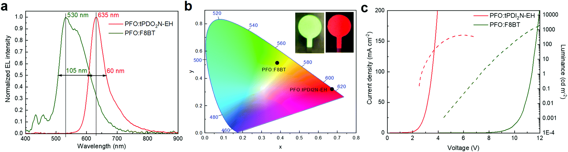
The electroluminescence (EL), CIE, and current–voltage–luminance characteristics of standard PFO:F8BT (19:1 ratio) and optimized PFO:tPDI2N-EH-based (2:18 ratio) OLEDs are shown in Fig. 4 and Table 3. PFO:F8BT-based OLEDs demonstrated the maximum LE of 1.24 cd A−1, PE of 0.4 lm W−1 and brightness of 1950 cd m−2 with white-green spectrum at maximum of 530 nm, full width at half maximum (FWHM) of 105 nm, and CIE coordinates located at (x, y) = (0.383, y = 0.514). This data is well aligned with literature.33,36 Using tPDI2N-EH instead of F8BT with PFO shifts the EL to red, which agrees well with the PL of tPDI2N-EH. The PFO:tPDI2N-EH-based OLEDs exhibit a narrow peak of EL with the maximum emission at 635 nm and FWHM of 60 nm with the CIE coordinates of (x, y) = (0.672, 0.321). Moreover, using tPDI2N-EH decreases the turn-on voltage to 2.6 V due to the lower LUMO energy level and more facile injection of electrons from the contacts into the active layer.
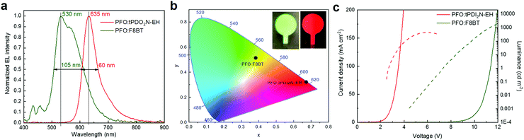 |
| | Fig. 4 (a) Normalized electroluminescence (EL) and (b) color coordinates spectra, (c) current–voltage–luminance characteristics of PFO:F8BT (ratio 19:1) and PFO:tPDI2N-EH (ratio 2:18) blends. | |
Table 3 Summary of device performance for OLEDs based on PFO:F8BT and PFO:tPDI2N-EH-blend films spin-coated on glass
| Emitting layer |
Ratioa |
V
on
[V] |
EQEmaxc [%] |
LEmaxd [cd A−1] |
PEmaxe [lm W−1] |
L
max
[cd m−2] |
|
PFO:F8BT or PFO:tPDI2N-EH ratio.
Turn on voltage was determined at the brightness of 1 cd m−2.
EQE – external quantum efficiency.
LE – luminous efficiency.
PE – power efficiency.
L
max – maximum of luminous.
|
| PFO:F8BT |
19:1 |
7.3 |
0.406 |
1.24 |
0.376 |
1951.6 |
| PFO:tPDI2N-EH |
2:18 |
2.6 |
0.057 |
0.046 |
0.031 |
435.4 |
2.3 OLEDs – slot-die coated devices
The roll-to-roll compatibility of organic and inorganic layers of OLED devices is an important consideration for large-scale fabrication methods.7 Thus, we aimed to repeat our best spin-coated devices with a slot-die coating technique. A FOM Nano Roll Coater (slot-die head with 13 mm shim width) was used to coat both the PEDOT:PSS interlayer and PFO:tPDI2N-EH (2:18) EML onto a PET/ITO substrate/anode base. The PEDOT:PSS interlayer was slot-die coated with the coating speed of 0.1 mm−1, dispensing rate of 12 μL min−1, and substrate temperature of 50 °C. The layer was thermally annealed at 100 °C for 15 min prior to the deposition of the EML. The PFO:tPDI2N-EH (2:18) solutions were coated from toluene at 30 mg mL−1 with the coating speed of 0.3 mm−1, dispensing rate of 30 μL min−1 at room temperature. The films were then dried in air at 100 °C for 30 minutes. A LiF/Ag electrode was thermally deposited using a thermal evaporation system through a shadow mask under a base pressure of ∼2 × 10⁻⁶ Torr (this top electrode was used for consistency in comparing to the spin-coated OLEDs). The device area was 160 mm2 as defined by the overlapping area of the ITO films and top electrodes. The optical absorption spectra of the roll-to-roll coated devices (in comparison to the spin-coated ones) can be found in the ESI† (Fig. S3).
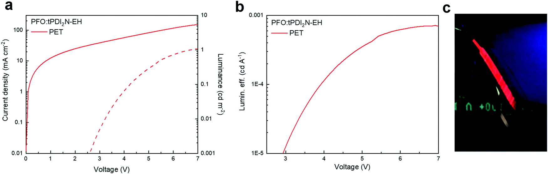
The current–voltage–luminance characteristics and LE versus current density of OLED devices with the PEDOT:PSS and PFO:tPDI2N-EH layers roll-to-roll coated on PET are shown in Fig. 5 and electrophysical parameters are summarized in Table 4. The OLED had a turn-on voltage of 6.6 V and maximum brightness of 1.1 cd m−2, demonstrating a fully functioning large area, roll-to-roll compatible coated device. Thus, this work shows that large-area OLEDs can be fabricated using slot-die coating techniques. The synthesis of new PDIs with high quantum yield and narrow peak luminescence of films, and optimized roll-to-roll coating of OLED layers is a viable pathway towards developing high-performance OLEDs for large-scale manufacturing.
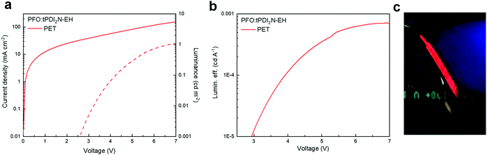 |
| | Fig. 5 (a) Current–voltage–luminance characteristics and (b) luminous efficiency (lumin. eff.) versus current density (LE–J, cd A−1) of PFO:tPDI2N-EH roll-to-roll coated on PET. (c) Photo of electroluminescent of PFO:tPDI2N-EH OLEDs on PET. | |
Table 4 Summary of device performance for slot-die coating OLEDs based on PFO:tPDI2N-EH-blend films
| Emitting layer |
Substrate |
V
on
[V] |
EQEmaxc [%] |
LEmaxd [cd A−1] |
PEmaxe [lm W−1] |
L
max
[cd m−2] |
|
PFO:tPDI2N-EH ratio is 2:18.
Turn on voltage was determined at the brightness of 1 cd m−2.
EQE – external quantum efficiency.
LE – luminous efficiency.
PE – power efficiency.
L
max – maximum of luminous.
The EML prepared from a solvent of toluene by roll-to-roll coated with the active area 160 mm2.
|
| PFO:tPDI2N-EHa |
PET/ITOg |
6.6 |
0.000147 |
0.000718 |
0.000054 |
1.1 |
3. Conclusion
We have presented electrically pumped, solution processed red OLEDs based on an N-annulated perylene diimide dimer as the emitting material. Use of the polyfluorene based polymer PFO as an additive for the red-emitter tPDI2N-EH resulted in large performance boosts with an optimal PFO:tPDI2N-EH ratio of 2:18 identified. The best efficiencies of PFO:tPDI2N-EH-based OLEDs exhibited a maximum LE of 0.05 cd A−1, power efficiency (PE) of 0.03 lm W−1 and external quantum efficiency (EQE) of 0.06%, and are among the best for PDI-based OLEDs. Proof-of-concept large-scale fabrication of OLEDs was demonstrated by roll-to-roll compatible coating of both the PEDOT:PSS hole injection layer and PFO:tPDI2N-EH emitting layer of OLEDs with large area (160 mm2) on plastic substrates. This work highlights the potential of N-annulated perylene diimide based materials to deliver commercially relevant advanced lighting devices.
Conflicts of interest
There are no conflicts to declare.
Acknowledgements
GCW acknowledges CFI JELF (34102), CRC, WED, and the University of Calgary. SVD is grateful for a MITACS fellowship. Authors would like to thank GenOptic LED Inc. for their financial support.
References
- H.-W. Chen, J.-H. Lee, B.-Y. Lin, S. Chen and S.-T. Wu, Light Sci. Appl., 2018, 7, 17168 CrossRef CAS PubMed.
- J. Ràfols-Ribé, P.-A. Will, C. Hänisch, M. Gonzalez-Silveira, S. Lenk, J. Rodríguez-Viejo and S. Reineke, Sci. Adv., 2018, 4, eaar8332 CrossRef PubMed.
- N. B. Kotadiya, P. W. M. Blom and G.-J. A. H. Wetzelaer, Nat. Photonics, 2019, 13, 765–769 CrossRef CAS.
- K. Guo, H. Wang, Z. Wang, C. Si, C. Peng, G. Chen, J. Zhang, G. Wang and B. Wei, Chem. Sci., 2017, 8, 1259–1268 RSC.
- S. Sato, S. Ohisa, Y. Hayashi, R. Sato, D. Yokoyama, T. Kato, M. Suzuki, T. Chiba, Y. Pu and J. Kido, Adv. Mater., 2018, 30, 1705915 CrossRef PubMed.
- B. R. Lee, E. D. Jung, J. S. Park, Y. S. Nam, S. H. Min, B.-S. Kim, K.-M. Lee, J.-R. Jeong, R. H. Friend, J.-S. Kim, S. O. Kim and M. H. Song, Nat. Commun., 2014, 5, 4840 CrossRef CAS PubMed.
- A. Sandström, H. F. Dam, F. C. Krebs and L. Edman, Nat. Commun., 2012, 3, 1002 CrossRef PubMed.
- C. Amruth, M. Z. Szymański, B. Łuszczyńska and J. Ulański, Sci. Rep., 2019, 9, 8493 CrossRef PubMed.
- V. G. Sree, H. Park, W. Cho and S.-H. Jin, Mol. Cryst. Liq. Cryst., 2017, 654, 73–82 CrossRef CAS.
- S. Burns, J. MacLeod, T. Trang Do, P. Sonar and S. D. Yambem, Sci. Rep., 2017, 7, 40805 CrossRef CAS PubMed.
- N. Aizawa, Y.-J. Pu, M. Watanabe, T. Chiba, K. Ideta, N. Toyota, M. Igarashi, Y. Suzuri, H. Sasabe and J. Kido, Nat. Commun., 2014, 5, 5756 CrossRef PubMed.
- Q. Wei, N. Fei, A. Islam, T. Lei, L. Hong, R. Peng, X. Fan, L. Chen, P. Gao and Z. Ge, Adv. Opt. Mater., 2018, 6, 1800512 CrossRef.
- Q. Zhang, H. Kuwabara, W. J. Potscavage, S. Huang, Y. Hatae, T. Shibata and C. Adachi, J. Am. Chem. Soc., 2014, 136, 18070–18081 CrossRef CAS PubMed.
- H. Xiang, J. Cheng, X. Ma, X. Zhou and J. J. Chruma, Chem. Soc. Rev., 2013, 42, 6128 RSC.
- Q. Zhao and J. Z. Sun, J. Mater. Chem. C, 2016, 4, 10588–10609 RSC.
- D. Schmidt, M. Stolte, J. Süβ, A. Liess, V. Stepanenko and F. Würthner, Angew. Chem., Int. Ed., 2019, 58, 13385–13389 CrossRef CAS PubMed.
- R. P. Sabatini, B. Zhang, A. Gupta, J. Leoni, W. W. H. Wong and G. Lakhwani, J. Mater. Chem. C, 2019, 7, 2954–2960 RSC.
- B. Zhang, H. Soleimaninejad, D. J. Jones, J. M. White, K. P. Ghiggino, T. A. Smith and W. W. H. Wong, Chem. Mater., 2017, 29, 8395–8403 CrossRef CAS.
- A. Laventure, C. R. Harding, E. Cieplechowicz, Z. Li, J. Wang, Y. Zou and G. C. Welch, ACS Appl. Polym. Mater., 2019, 1, 2168–2176 CrossRef CAS.
- F. Tintori, A. Laventure and G. C. Welch, ACS Appl. Mater. Interfaces, 2019, 11, 39010–39017 CrossRef CAS PubMed.
- A. Laventure, S. Stanzel, A.-J. Payne, B. H. Lessard and G. C. Welch, Synth. Met., 2019, 250, 55–62 CrossRef CAS.
- R. K. Gupta, A. Dey, A. Singh, P. K. Iyer and A. A. Sudhakar, ACS Appl. Electron. Mater., 2019, 1, 1378–1386 CrossRef CAS.
- G. Li, D. Li, X. Liu, H. Xu, J. Zhang, S. Wang, Z. Liu and B. Tang, Chem. Commun., 2019, 55, 9661–9664 RSC.
- D. Sun, D. Meng, Y. Cai, B. Fan, Y. Li, W. Jiang, L. Huo, Y. Sun and Z. Wang, J. Am. Chem. Soc., 2015, 137, 11156–11162 CrossRef CAS PubMed.
- J. Zhang, Y. Li, J. Huang, H. Hu, G. Zhang, T. Ma, P. C. Y. Chow, H. Ade, D. Pan and H. Yan, J. Am. Chem. Soc., 2017, 139, 16092–16095 CrossRef CAS PubMed.
- E. Kozma, W. Mróz, F. Villafiorita-Monteleone, F. Galeotti, A. Andicsová-Eckstein, M. Catellani and C. Botta, RSC Adv., 2016, 6, 61175–61179 RSC.
- G. Li, Y. Zhao, J. Li, J. Cao, J. Zhu, X. W. Sun and Q. Zhang, J. Org. Chem., 2015, 80, 196–203 CrossRef CAS PubMed.
- M. Matussek, M. Filapek, P. Gancarz, S. Krompiec, J. Grzegorz Małecki, S. Kotowicz, M. Siwy, S. Maćkowski, A. Chrobok, E. Schab-Balcerzak and A. Słodek, Dyes Pigm., 2018, 159, 590–599 CrossRef CAS.
- L. Zong, Y. Gong, Y. Yu, Y. Xie, G. Xie, Q. Peng, Q. Li and Z. Li, Sci. Bull., 2018, 63, 108–116 CrossRef CAS.
- S. V. Dayneko, A. D. Hendsbee and G. C. Welch, Small Methods, 2018, 2, 1800081 CrossRef.
- J. R. C. Smirnov, A. Sousaraei, M. R. Osorio, S. Casado, J. J. Hernández, L. Wu, Q. Zhang, R. Xia, D. Granados, R. Wannemacher, I. Rodriguez and J. Cabanillas-Gonzalez, npj Flexible Electron., 2019, 3, 17 CrossRef.
- J. H. Ahn, C. Wang, I. F. Perepichka, M. R. Bryce and M. C. Petty, J. Mater. Chem., 2007, 17, 2996 RSC.
- D. de Azevedo, J. N. Freitas, R. A. Domingues, M. M. Faleiros and T. D. Z. Atvars, Synth. Met., 2017, 233, 28–34 CrossRef CAS.
- K. Kwak, K. Cho and S. Kim, Sci. Rep., 2013, 3, 2787 CrossRef PubMed.
- M. Gioti, D. Kokkinos, C. I. Chaidou, A. Laskarakis, A. K. Andreopoulou, J. K. Kallitsis and S. Logothetidis, Phys. Status Solidi, 2016, 213, 2947–2953 CrossRef CAS.
- A. C. M. Colella, J. Griffin, J. Kingsley, N. Scarratt, B. Luszczynska and J. Ulanski, Micromachines, 2019, 10, 53 CrossRef PubMed.
- C. Würth, M. Grabolle, J. Pauli, M. Spieles and U. Resch-Genger, Nat. Protoc., 2013, 8, 1535–1550 CrossRef PubMed.
- F. J. Céspedes-Guirao, S. García-Santamaría, F. Fernández-Lázaro, A. Sastre-Santos and H. J. Bolink, J. Phys. D: Appl. Phys., 2009, 42, 105106 CrossRef.
Footnote |
| † Electronic supplementary information (ESI) available. See DOI: 10.1039/c9tc05584c |
|
| This journal is © The Royal Society of Chemistry 2020 |
Click here to see how this site uses Cookies. View our privacy policy here. 
 a,
Mohammad
Rahmati
b,
Majid
Pahlevani
*c and
Gregory C.
Welch
a,
Mohammad
Rahmati
b,
Majid
Pahlevani
*c and
Gregory C.
Welch