
 Open Access Article
 This Open Access Article is licensed under a Creative Commons Attribution-Non Commercial 3.0 Unported Licence
Application of ultrasonic sprayed zirconium oxide dielectric in zinc tin oxide-based thin film transistor†
Abayomi T.
Oluwabi
 *a,
Atanas
Katerski
a,
Emanuel
Carlos
b,
Rita
Branquinho
b,
Arvo
Mere
a,
Malle
Krunks
a,
Elvira
Fortunato
b,
Luis
Pereira
b and
Ilona
Oja Acik
*a
*a,
Atanas
Katerski
a,
Emanuel
Carlos
b,
Rita
Branquinho
b,
Arvo
Mere
a,
Malle
Krunks
a,
Elvira
Fortunato
b,
Luis
Pereira
b and
Ilona
Oja Acik
*a
aLaboratory of Thin Film Chemical Technologies, Department of Materials and Environmental Technology, Tallinn University of Technology, Ehitajate tee 5, 19086 Tallinn, Estonia. E-mail: abayomioluwabi@gmail.com; ilona.oja@ttu.ee
bCENIMAT/i3N Nova School of Science Technilogy (FCT-NOVA), Universidade NOVA de Lisboa and CEMOP/Uninova, Campus de Caparica, 2829-516 Caparica, Portugal
First published on 13th February 2020
Abstract
Solution processing of metal oxides has been the focal point of interest for many researchers mainly because of the cost effectiveness and improved properties of metal oxides. However, achieving uniform and high-quality film deposition has been a recurring challenge using various wet-chemical techniques. Herein, we report a fully solution-based fabrication process exploiting both the ultrasonic spray pyrolysis (USP) and spin coating techniques owing to their simplicity, high degree of freedom for mixing metal oxide precursor salt, and larger area deposition. An amorphous zirconium oxide (ZrOx) dielectric and zinc tin oxide (ZTO) semiconductor were deposited, respectively. The dielectric characteristics of the ZrOx thin films were accessed by fabricating MIS-devices for the samples deposited at 200 °C and 400 °C, which exhibited a capacitance of 0.35 and 0.67 μF cm−2 at 100 kHz and relative permittivity of 8.5 and 22.7, respectively. The ZrOx thin film was then integrated as the gate dielectric layer in ZTO solution-processed thin film transistors, exhibiting a high electrical performance with low hysteresis (−0.18 V), high on/off current ratio of 106 orders of magnitude, saturation mobility of 4.6 cm2 V s−1, subthreshold slope of 0.25 V dec−1, and operating at a low voltage window of 3 V. Based on these results, the as-fabricated ZTO/ZrOx TFT opens the potential application of solution-processed transistors for low-cost electronic devices.
1. Introduction
Metal oxide materials are an excellent class of materials with enormous electronic functionalities depending on their area of usefulness, either as an insulator or a semiconductor. Recently metal oxide thin films have attracted significant interest for future electronic applications especially in thin film transistors (TFTs) due to their large-area uniformity, high mobility, good optical transparency in the visible light region, thermal stability, and excellent environmental impact, and they can be produced at low cost.1–5 However, most of these metal oxide transistors are incorporated into traditional silicon dioxide (SiO2) dielectrics and they are operated at a high voltage window above 30 V, which hinder their use in low-voltage, smart and portable applications. Since the induced electric field directly corresponds to charge accumulation, replacing the SiO2 gate dielectric layer of TFTs with a high permittivity (high-κ) material would help accomplish low operation voltage. Furthermore, the scaling-down of electronic devices (below 100 nm) has also called for the need to replace the SiO2 gate dielectric layer because of the problem of leakage current caused by the quantum tunnelling effect.2,6 Also, at a lower thickness (10–100 nm), a high-κ gate dielectric can achieve high capacitance, allowing enough charge injection into the active layer of the transistor.2,7 Several inorganic high-κ oxides such as titanium dioxide (TiO2), zirconium dioxide (ZrO2),8,9 yttrium oxide (Y2O3), tantalum oxide (Ta2O5),10,11 hafnium oxide (HfO2)12,13 and aluminium oxide (Al2O3)14 have been investigated as attractive candidates to replace the SiO2 gate dielectric in TFTs. Barquinha et al.11 studied the behaviour and stability of transparent TFTs produced at low temperature using a multicomponent amorphous dielectric material. Their findings revealed that the Ta2O5 dielectric can help to improve the device performance based on the fact that this material has the tendency to increase amorphization when mixed with other dielectric materials with lower permittivity.Among the inorganic high-κ dielectrics, zirconium oxide (ZrOx) is a desirable gate insulator because bulk ZrO2 has a high permittivity value (∼25), low leakage current, good thermal stability, adequate band alignment and forms good adhesion with Si-substrates.3,15 Most importantly, the wide bandgap (5.0–7.8 eV) of ZrOx is beneficial to suppress charge penetration from the gate electrode and to reduce the generation of charge as a result of the thermal/photoexcitation process.8 In the past, good quality ZrOx thin films have been deposited using different methods, for example, atomic layer deposition, sputtering, chemical vapour deposition, and e-beam evaporation,16 but these methods are very expensive and the growth rate of the thin film is time consuming due to the high vacuum. As opposed to the vacuum-based methods, solution-based method such as spin coating, dip coating, inkjet printing, and spray pyrolysis (SP) offer additional advantages including cost effectiveness, simplicity, high degree of freedom, and larger area of deposition.5,9,11–19
Interestingly, among the many wet-chemical methods, ultrasonic spray pyrolysis (USP) is an excellent thin film deposition technique, offering an easy deposition process that gives room for free mixing of precursor solutions at the molecular level before deposition. The cost-effectiveness and non-selective tendency to any substrate of USP distinguish it among several other solution processes. It can easily be scaled up for industrial or commercial fabrication processes and still maintain good film uniformity over a wide area.18,20 Ortiz et al.21 fabricated a cubic phase of ZrOx thin film by SP, and Oluwabi et al.17,20 reported the deposition of a ZrOx thin film by USP. Wang et al.22 reported that a ZrOx dielectric deposited by SP has a low leakage current (1.2 × 10⁻⁷ A cm−2) and a high dielectric breakdown of 9.5 MV cm−1 at a substrate temperature below 350 °C.
Moreover, to achieve reliable TFTs, the optimum band offset between the conduction band of the dielectric in an n-type transistor device must be above 1 eV with respect to that of the channel layer in order to reduce the leakage caused by the Schottky effect,2,23 and ZrOx can help prevent such effect. Owing to its physical and chemical properties, ZrOx has been employed in various TFTs, such as MoS, organic, graphene and oxide TFTs.24–26 As part of the TFT, the channel layer is significant especially in transparent amorphous semiconductors, as suggested by Honoso et al.27 Although solution-processed metal oxide semiconductors, namely, indium zinc oxide (IZO) and indium gallium zinc oxide (IGZO), have been reported as attractive choices of the channel layer, indium-free semiconductors such as zinc tin oxide (ZTO), among others have also attracted significant attention due to the scarcity of naturally available indium resources,27,29 enabling competitive device performance in comparison with their indium-based counterparts.28,30 The ZTO semiconductor has good applicability in TFT, but typically requires a high deposition temperature (above 350 °C), and the mechanism of its synthesis has not been fully comprehended. Salgueiro et al.31 reported the role organic solvents in the performance of solution-processed zinc tin oxide (ZTO)-based TFTs. Table 1 presents the reported solution-processed ZrOx dielectric TFTs. Adamopoulos et al.32 reported a fully solution-processed TFT by SP with a ZrOx gate dielectric operating at a low voltage with high mobility. Similarly, Xinge et al.22 fabricated a fully solution-processed TFT by spray combustion synthesis (SCS) to achieve a device with high carrier mobility and good reliability. Also, several solution-processed ZrOx dielectric TFTs have been reported via spin coating.3,25,26,33
| Gate dielectric layer | Channel layer | Transistor parameters | Ref. | ||||||||
|---|---|---|---|---|---|---|---|---|---|---|---|
| Method | Material | T (°C) | Structure | Method | Material | T (°C) | Structure | Mobility (cm2 V−1 S−1) | V on (V) | SS (V dec−1) | |
| Spin coating | ZrOx | 400 | Crystalline | Spin coating | InOx | 300 | Crystalline | 4.42 | 0.31 | 0.07 | 3 |
| Spin coating | ZrOx | 300 | Amorphous | Spin coating | NiOx | 250 | Amorphous | 4.8 | −1.6 | 0.35 | 8 |
| Spin coating | ZrOx | 250 | Amorphous | Spin coating | InOx | 250 | Amorphous | 10.0 | 0 | 0.1 | 8 |
| Spin coating | ZrOx | 500 | Crystalline | Spin coating | ZTO | 500 | Crystalline | 2.50 | 1 | 0.23 | 34 |
| Spin coating | ZrOx | 350 | Amorphous | Spin coating | IZO | 250 | Amorphous | 0.16 | 0 | 1.49 | 26 |
| Spin coating | ZrOx | 400 | Crystalline | Spin coating | SnOx | 350 | Crystalline | 2.50 | −0.5 | 0.30 | 33 |
| SCS | ZrOx | 350 | Amorphous | SCS | IGZO | 350 | Amorphous | 28.5 | 0.3 | — | 22 |
| Spray pyrolysis | ZrOx | 400 | Crystalline | Spray pyrolysis | ZnO | 400 | Crystalline | 32.0 | −1 | — | 32 |
| Spray pyrolysis | ZrOx | 400 | Amorphous | Spin coating | ZTO | 350 | Amorphous | 4.60 | −0.9 | 0.25 | Present study |
In this work, we demonstrate a combination of ultrasonic spray pyrolysis (USP) and spin coating in the fabrication of high-quality ZrOx gate dielectrics and ZTO semiconductor, respectively, onto a rigid substrate. To the best of our knowledge, this is the first report of an all-amorphous oxide TFT with low operational voltage. Furthermore, the introduction of USP into our device fabrication process allowed the fabrication of the TFT over a larger area, it improved the properties of the gate dielectric layer and eliminated the problem of pinholes, which have the tendency to jeopardise the final performance of the TFT device. In our previous publication, ZrOx thin films were tested only as a capacitor, but herein, we further tested a ZrOx thin film with a thickness of ∼30 nm as both a capacitor and gate dielectric in TFTs, which is considerably lower than the thickness of ZrOx in our previous report.17,18,20
2. Experimental details
2.1 Precursor solution preparation
The ZrOx precursor solution was prepared by dissolving zirconium(IV) acetyl acetonate (Zr(C5H7O2)4; Sigma-Aldrich, 98%) in methanol (Me–OH, CH3OH; Sigma-Aldrich, 99%) at room temperature to yield a solution with a Zr4+ ion concentration of 0.025 M, and the solution was constantly stirred for at least 30 min to ensure complete dissolution of the solute in the solvent. The solution was completely transparent and remained transparent even after aging.The zinc oxide precursor solution was prepared by dissolving zinc nitrate salt (zinc nitrate hexahydrate; Sigma-Aldrich, 98%) in 2-methoxyl ethanol (ME) (Roth, 98%). The tin oxide precursor was prepared from a tin chloride source (tin(II) chloride; Sigma-Aldrich, 98%) dissolved in ME solvent. Both the zinc and tin oxides solutions were prepared at a metal ion concentration of 0.1 M and stirred for about 12 h. The ZTO precursor was made by mixing the corresponding zinc and tin oxide precursor solutions in the ratio of 2![[thin space (1/6-em)]](https://www.rsc.org/images/entities/char_2009.gif) :1. The resulting solution was then stirred for 1 h to ensure homogeneity and finally filtered through a hydrophilic filter with a 0.20 μm pore size before use.
:1. The resulting solution was then stirred for 1 h to ensure homogeneity and finally filtered through a hydrophilic filter with a 0.20 μm pore size before use.
The ZTO precursor solution was characterized by thermogravimetry and differential scanning calorimetry (TG-DSC) analysis of the 0.1 M solution of the ZTO precursor to account for methoxy propanol solvent evaporation events. TG-DSC analyses were performed under an air atmosphere up to 550 °C with a 10 °C min−1 heating rate in an aluminium crucible using a simultaneous thermal analyser (TG-DSC – STA 449 F3 Jupiter, Netzsch).
2.2 Thin film deposition and characterisation
Prior to the film deposition, all substrates (p-type silicon wafer and quartz with 2 × 2 cm2) were rinsed in an ultrasonic bath at 60 °C in acetone, isopropanol, and distilled water for 15 min respectively, and were later dried in air. ZrOx dielectric films were deposited via the ultrasonic spray pyrolysis (USP) technique as shown in Fig. 1a, and the deposition parameters have been reported in.17 For the purpose of this study, the films were deposited at both 200 °C and 400 °C without further annealing.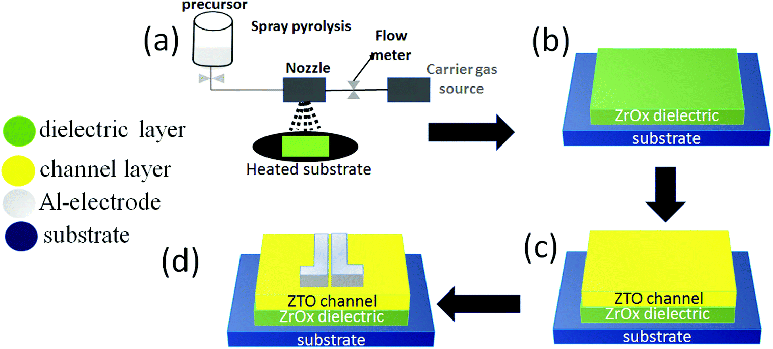 | ||
| Fig. 1 Fabrication stages of ZrOx gate dielectric TFT devices with ZTO semiconductor layer: (a) spraying of ZrOx precursor solution, (b) deposition of ZrOx dielectric onto Si-substrate, (c) spin coating ZTO semiconductor onto ZrOx/Si, and (d) aluminium electrode deposition, yielding a TFT device with the channel width (W) of 1400 μm and length of 100 μm (W/L = 14). | ||
The film structure was assessed by glancing angle X-ray diffraction (GAXRD) performed on an X’Pert PRO PANalytical powder diffractometer using Cu Kα line radiation (λ = 1.540598 Å) with the angle of incidence of the X-ray beam fixed at 0.9°. The thickness of ZTO and ZrOx was obtained by spectroscopic ellipsometry measurement in the energy range of 1.5–6.0 eV with an incident angle of 70° using a Jobin Yvon Uvisel system. Total transmittance spectra were obtained using a Jasco-V670 spectrophotometer equipped with an integrating sphere in the wavelength range of 200–800 nm, which was later used to calculate the optical bandgap of the ZrOx dielectric at different deposition temperatures. Surface morphology was studied using a ZEISS HR Ultra 55 scanning electron microscope (SEM). The acceleration voltage for SEM measurements was 4.0 kV. Attenuated total reflectance (ATR) Fourier transform infrared spectroscopic characterization of the thin films deposited on silicon substrates was performed in the range of 4500–560 cm−1.
2.3 Fabrication of ZrOx MIS devices
The dielectric characteristics of ZrOx were accessed through metal–insulator–semiconductor (MIS) capacitors by depositing the ZrOx thin film onto p-type silicon substrates (1–3 Ω cm), as described above. Al gate electrodes (80 nm thick) with an area of 8.0 × 10⁻³ cm2 were deposited by thermal evaporation via a shadow mask, and a similar thickness of Al film was also deposited on the back of the silicon wafer to improve the ohmic conductivity. Electrical characterization was performed by measuring both the current–voltage (I–V) and capacitance–voltage (C–V) characteristics of the devices using a semiconductor device analyser (Keysight 1500A) connected to a Casecade M150 microprobe station inside a dark box at room temperature with humidity between 30% and 40%. The capacitance–frequency (C–F) curve was obtained from the impedance data measured in the range of 10 Hz to 1 MHz using an AUTOLAB PGSTAT30/2.2.4 Fabrication of ZrOx TFT devices
TFTs were produced in a staggered bottom-gate, top-contact architecture by depositing the ZrOx thin films onto p-type silicon substrates, as described above and shown in Fig. 1a and b. The ZTO active layer was later deposited by spin coating (using a Laurell Technologies instrument). Four layers of 0.1 M ZTO precursor solution was spun for 35 s at 2000 rpm onto the ZrOx thin films and annealed at 150 °C, 250 °C, and 350 °C for 30 min (Fig. 1c). Finally, the source and drain aluminum electrodes (100 nm thick) were deposited by thermal evaporation via a shadow mask onto the annealed films (Fig. 1d). The output and the transfer characteristics of the devices were obtained in continuous mode with both back and forth sweeps recorded in ambient conditions inside a Faraday cage (in dark conditions) using a semiconductor parameter analyzer (Agilent 4155C).The saturation mobility (μsat) was determined from the following equation:14
 | (1) |
3. Results and discussion
3.1 ZrOx dielectric thin film characterisation
The surface morphology of the ZrOx dielectric films deposited at different temperatures was observed via atomic force microscope (AFM, Fig. 2a and c) and SEM analysis (Fig. 2b and d). The films surface roughness was estimated from the AFM height profile and scanned through an area of 1 μm × 1 μm. The ZrOx films deposited at 200 °C (Fig. 2a) demonstrated a higher surface roughness with a root mean square (RMS) roughness value of 0.33 nm compared with that deposited at 400 °C with an RMS value of 0.29 nm. The decrease in the film surface roughness at higher temperature could be due to film densification, which was aided by the decomposition of volatile organic precursor during the spray pyrolysis process. According to the TG/DTG/DTA results of Oja et al.35,36 for spray-deposited TiO2 dielectrics, the complete decomposition of volatile organic complexes occurs above 400 °C. In addition, the deposited ZrOx films were structurally amorphous (see Fig. S1 in the ESI†) as confirmed by X-ray diffraction. Furthermore, as depicted by the SEM images (Fig. 2b and d), the ZrOx dielectric films were uniform, compact, and very smooth.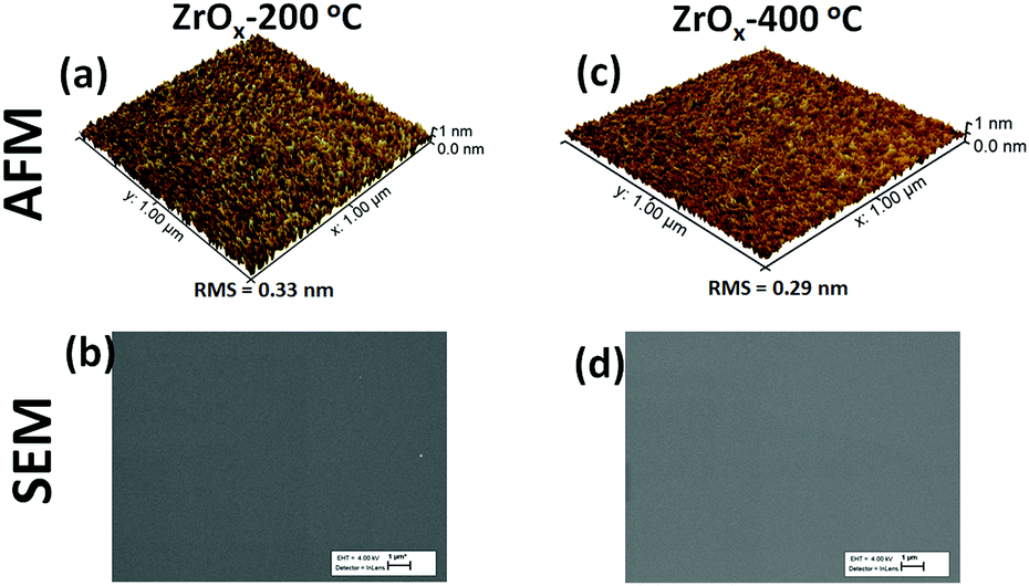 | ||
| Fig. 2 Surface morphology of the solution-processed ZrOx dielectric films. AFM deflection images of the as-deposited ZrOx dielectric at both (a) 200 °C, and (c) 400 °C; and their corresponding SEM images at (b) 200 °C and (d) 400 °C on an Si-substrate. | ||
The FT-IR spectra of the deposited ZrOx dielectric thin films deposited at 200 °C and 400 °C on Si-substrates is shown in Fig. 3. All the films show a sharp infrared absorbance peak at 1120 cm−1, which can be ascribed to the optical stretching of the Si–O bond from the Si-substrate. The asymmetric CH3 deformation vibration centred at 1430 cm−1 was observed and a slightly broad peak at 3545 cm−1 associated with the bending and stretching vibrational bond of the native O–H group from the adsorbed water molecules on the surface of the ZrOx dielectric was also observed.13
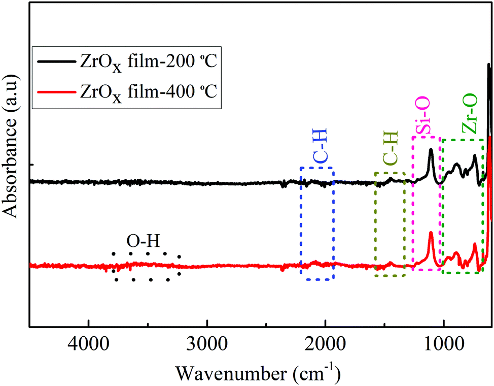 | ||
| Fig. 3 FTIR ATR absorbance spectra of ZrOx dielectric films deposited at 200 °C and 400 °C. | ||
Furthermore, a weak absorbance peak centred at 2110 cm−1 corresponding to the C–H bond stretching was observed for both films, which can be ascribed to the organic residues from the ZrOx precursor reagent; thereby suggesting the presence of organic residue in the ZrOx dielectric film network even after annealing at 400 °C. Both the ZrOx dielectric films deposited at 200 °C and 400 °C exhibited infrared absorption peaks centred at 880, 750, and 945 cm−1, which are related to the metal oxygen bond (Zr–O) stretching.13,31
The optical transmittance of the as-deposited ZrOx dielectric film at 200 °C and 400 °C is shown in Fig. 4a. The absence of interference fringes on the transmittance spectra indicates that the films are very thin, which was later confirmed by spectroscopic ellipsometry (∼20 nm and ∼30 nm thick for the 200 °C and 400 °C deposited films, respectively). It was observed that both deposited ZrOx dielectric films demonstrated a high optical transparency in the visible region (350–700 nm) with a percentage transmittance of above 80%.
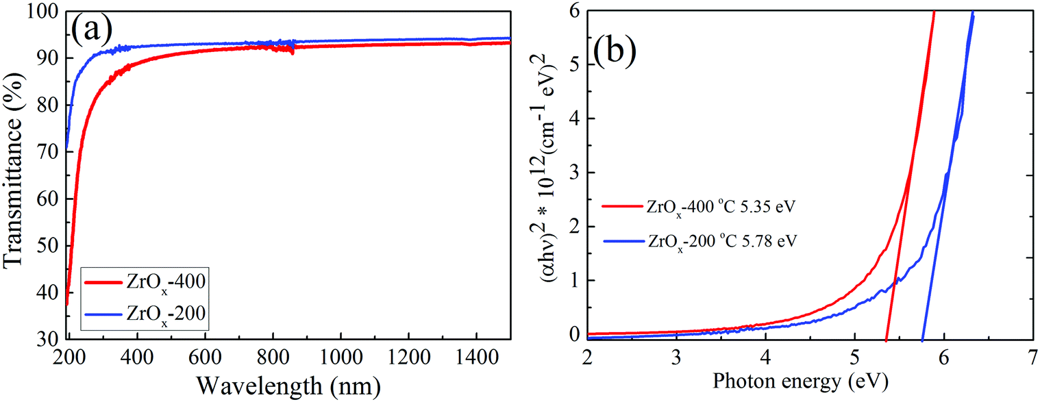 | ||
| Fig. 4 (a) Total transmittance spectra of the ZrOx dielectric film deposited at 200 °C and 400 °C and (b) corresponding bandgap extrapolation in the Tauc plots. | ||
In addition, the transmittance decreased with an increase in the deposition temperature, which can be attributed to the changes in the film microstructure, although it was impossible to be detected by XRD since the films are amorphous according to the XRD result (ESI† S1, XRD). Another reason may be because of the removal of oxygen vacancies in the film when they were grown at 400 °C. A similar tendency was reported in our previous publication.8,17 The optical bandgap (Eg) was estimated by fitting the transmittance spectra to the standard Tauc plot,37 which was determined to be 5.78 and 5.35 eV for the ZrOx films deposited at 200 °C and 400 °C, respectively (Fig. 4b). The reduction in the Eg value with the deposition temperature can be attributed to many reasons, including microstructural changes within the film, the presence of localised defects within the ZrOx band structure thereby causing a reduction in the Eg value, and the disordered nature of the amorphous materials.3,8,17 Nevertheless, the Eg values being generally high above 5 eV is a good indication that the spray-deposited ZrOx dielectric film would provide enough barrier needed to prevent carrier conduction between the active layer and the gate dielectric layer of TFT.
3.2. ZrOx MIS characterisation
To demonstrate the insulating property of the sprayed ZrOx dielectric thin film, an MIS-capacitor with the Al/p-Si/ZrOx/Al structure was fabricated. The capacitance–frequency (C–F) dispersion curves in Fig. 5a show that the area capacitance at 100 kHz for the ZrOx dielectric film deposited 200 °C and 400 °C is 0.37, 0.67 μF cm−2, corresponding to a permittivity of 8.4 and 22.7, respectively. The observed increase in the permittivity value of the 400 °C deposited film can be due to the densification of the film at a higher temperature. An important point is that the observed increase in the dispersion curve for ZrOx deposited at 200 °C as the frequency decreases may be an indication that there is another dielectric relaxation mechanism at lower frequencies related with mobile ionic species as a result of the incomplete decomposition of the ZrOx precursors at a low temperature.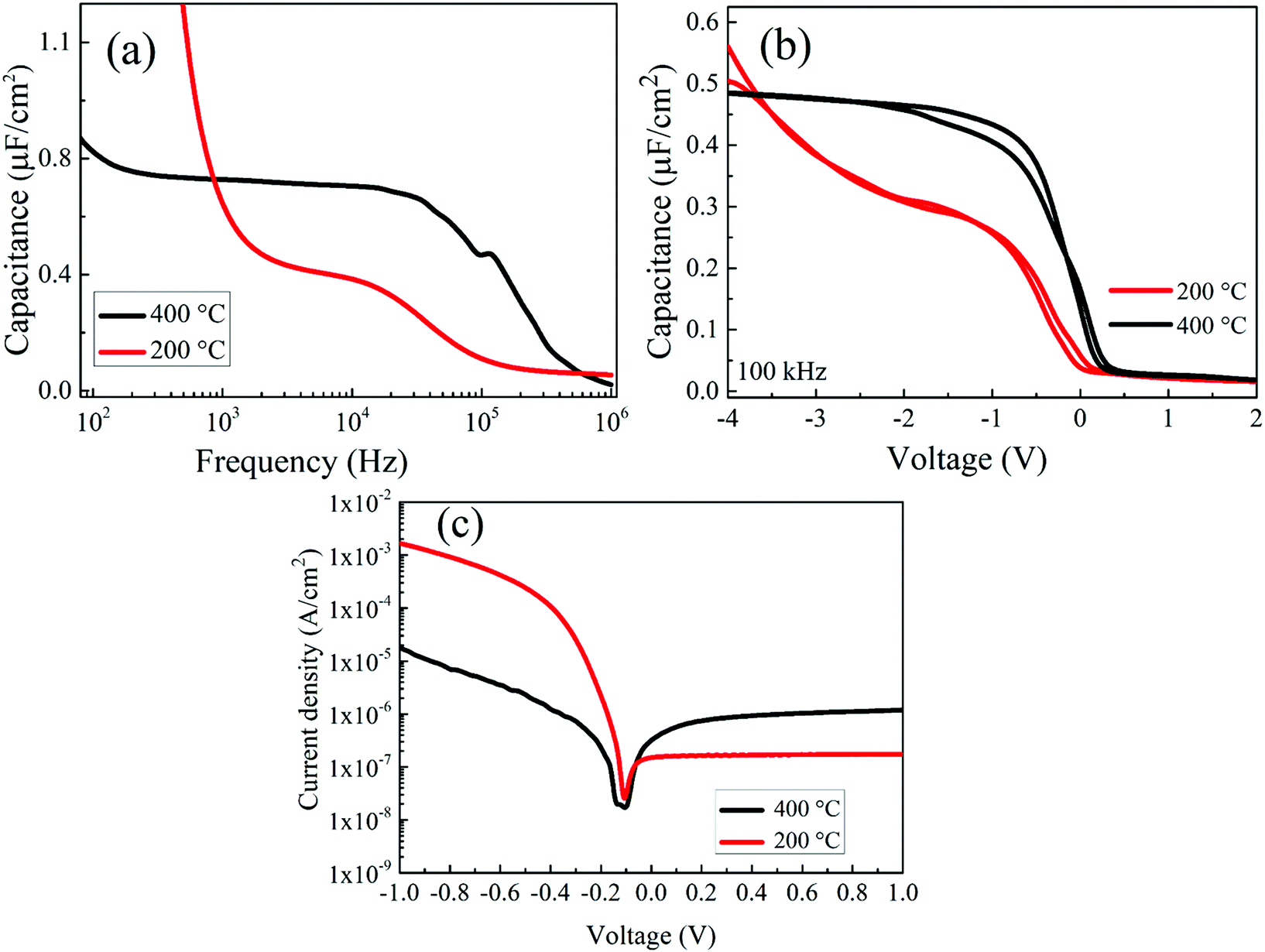 | ||
| Fig. 5 (a) Capacitance–frequency curve, (b) capacitance–voltage, and (c) current–voltage characteristics of Al/p-type Si/ZrOx/Al MIS capacitors with the ZrOx films obtained at various deposition temperatures. | ||
Fig. 5b shows the capacitance–voltage curves for both the 200 °C and 400 °C deposited ZrOx dielectric films. The voltage bias was carried in the forward and reverse sweep at 100 kHz, to ascertain the stability of the MIS capacitor. When the ZrOx film was deposited at 400 °C, there was a saturation of the capacitance in the accumulation regime, which did not occur for that at 200 °C due to the leakage current (as confirmed in Fig. 5c). Moreover, and contrary to that for the film deposited at 200 °C, there are no bumps when reaching accumulation, indicating a reduction in the density of electron trap sites at the interface between ZrOx–silicon. Depending on the type of shift in the C–V curve, an understanding about the charge trapping/de-trapping within the oxide band structure can be obtianed.14 In our case, the device produced at 200 °C showed that a more negative bias was needed to complete accumulation due to electron trapping, corroborating the C–F results.
Fig. 5c shows the plot of the current density against voltage for the 200 °C, and 400 °C deposited ZrOx dielectrics. From the plot, the leakage behaviour of the ZrOx gate dielectric films was estimated from in the reverse bias regime at 1 V. It was observed that the ZrOx deposited at 400 °C has a lower leakage current of 3.56 × 10⁻⁶ A cm−2 that is lower than the one measured for the 200 °C deposited dielectric film (4.26 × 10⁻⁴ A cm−2). The observed decrease in the leakage current is 2 orders of magnitude and can be attributed to the decomposition of volatile organic compounds in the film at higher temperature, resulting in the improvement of the density of the dielectric films.8,17
3.3 ZTO semiconductor thin film formation and characterisation
The semiconductor, ZTO, film was formed via a simple sol–gel synthesis approach, and the ZTO precursor is a mixture of both Zn-nitrate and Sn-chloride salts and dispersed in ME at a mole ratio of 2:1 at room temperature. The thermal gravimetry and differential calorimetry analyses for both the Zn–nitrate and the Sn–chloride precursor solution were studied and are presented in Fig. S2(a) and (b), ESI,† respectively. The degradation of the Zn–nitrate precursor is very fast with almost 80% degradation below 200 °C, while the degradation of the Sn-precursor is fairly slow requiring a minimum temperature of 400 °C to complete the decomposition process. On the other hand, the gravimetric and differential scanning calorimetry analyses for the ZTO precursor solution is presented in Fig. S3(a and b), respectively, and the total residual mass loss for the decomposition process from 20–550 °C is 70.28%. Thus, to obtain the desired ZTO thin film phase, the reaction is expected to occur at a much higher temperature (preferably, above 400 °C).
The FTIR spectrum of the ZTO precursor solution made from the ME solution is presented in [S5] and the FTIR spectra of the ZTO semiconductor thin films produced from this solution at various annealing temperatures are presented in Fig. 6a. All the ZTO semiconductor films show a sharp infrared absorbance peak at 1120 cm−1, which can be related to the optical stretching of the Si–O bond from the Si-substrate, and they equally exhibited infrared absorption peaks centred at 880, 750, and 945 cm−1, corresponding to the metal oxide bond (Zn–O and Sn–O) stretching.13,31 This result indicates that the ZTO films were composed of some metal oxygen bonds and organic residues. The microstructures of the ZTO thin films at various annealing temperatures were measured using XRD, and the results are shown in Fig. 6b. The absence of obvious peaks in the X-ray diffraction patterns demonstrate the amorphous nature of the ZTO thin films.
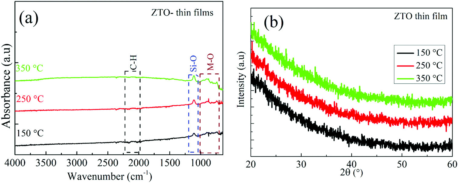 | ||
| Fig. 6 (a) FTIR spectra of the ZTO semiconductor thin films annealed at various temperatures. (b) XRD patterns of the ZTO semiconductor thin films annealed at various temperatures. | ||
3.4 Electrical properties of solution-processed TFTs based on SiO2 gate dielectric
Based on the above discussion on the properties of the ZrOx thin film, it can be inferred that the films deposited at a higher temperature displayed better dielectric characteristics. Nevertheless, to juxtapose this behaviour in TFTs, we first investigated the feasibility of a solution-processed ZTO active layer in a bottom gate and top source/drain contact architecture. The conventional SiO2/Si-substrate was used as the gate electrode and gate dielectric because of its reliability and low defect density. Fig. 7 shows the output and the transfer characteristics of the solution-processed ZTO-TFT and scheme of the TFT architecture. The output curve of the ZTO-TFT after annealing at 350 °C shows that the device has a clear distinction between the linear and the saturation regimes (Fig. 7a). The absence of overcrowding data points at the low drain voltage region demonstrates the excellent ohmic contact between the Al electrode and the ZTO channel layer. The TFT trans-conduction characteristics are depicted in Fig. 7b, which showed very little hysteresis during the sweep of the gate voltage in both the forward and reverse directions. The result of the saturation mobility was extracted by fitting the transconductance curve to eqn (1), and the statistical summary of both the TFT and MIS devices is presented in Table S1 (ESI†). The calculated saturation mobility (μsat) is ∼0.5 cm2 V−1 s−1, the threshold voltage (Vth) is 1.3 V, the on–off current ratio (Ion/Ioff) is up to 108, the sub-threshold swing (S.S.) is 760 mV per decade, the hysteresis is −0.4 V, and the on-voltage (Von) is −0.5 V. The extracted device parameters are also summarised in Table 2. The SS value was used to estimate the density of the interface state (Dit) of 1.1 × 1012 cm2 for the ZTO-TFT device using eqn (2):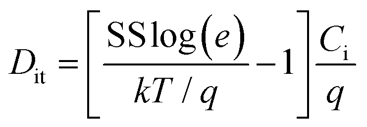 | (2) |
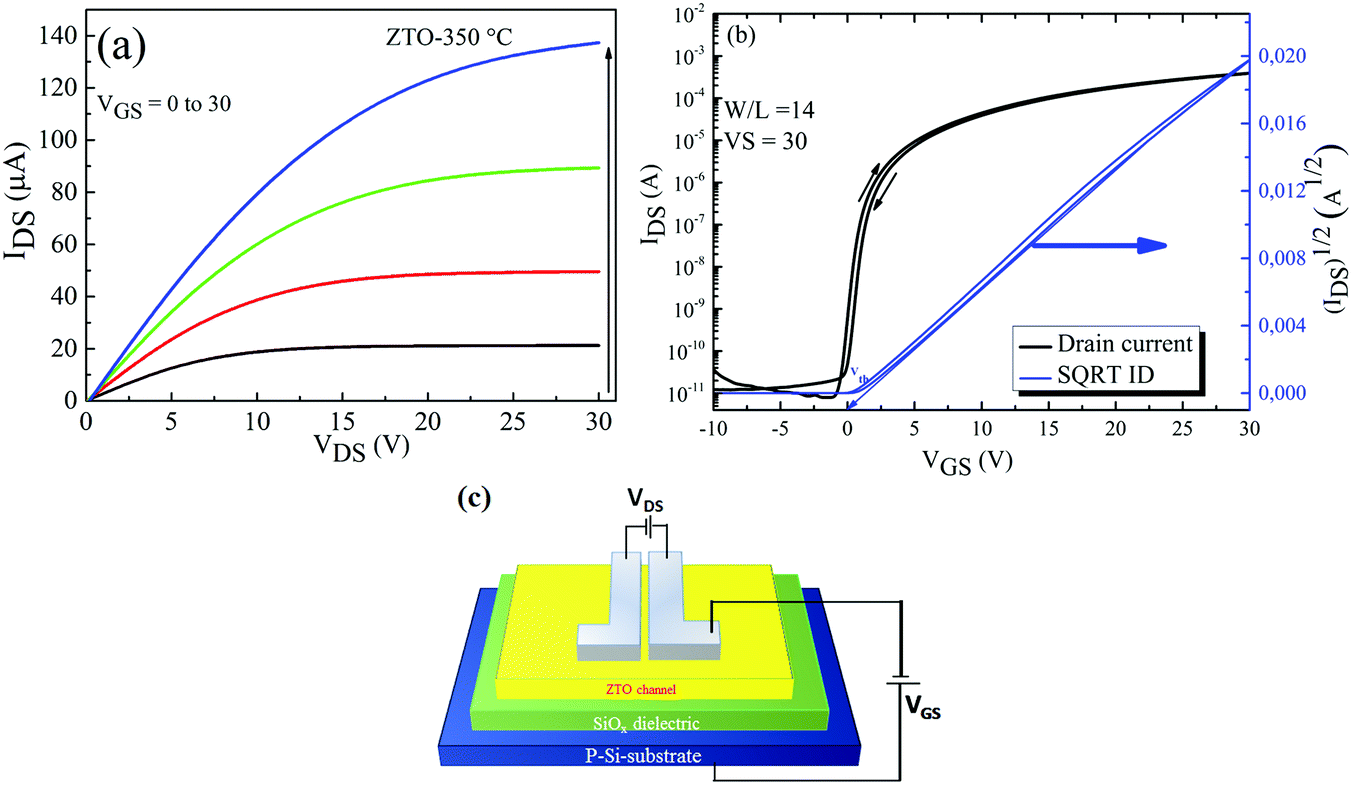 | ||
| Fig. 7 TFT characteristics of the ZTO-350/SiO2 device. (a) Output, and (b) transfer performance; while a schematic representation of the device structure is shown in (c). | ||
| Device | V on (V) | I on/Ioff | Sat. mob. (cm2 V−1 s−1) | V Th (V) | SS (V dec−1) | Hysteresis (V) | D it (cm−2) |
|---|---|---|---|---|---|---|---|
| ZTO-250/SiOx | 7.80 ± 0.2 | ∼104 | — | ∼8.45 | — | 1.71 ± 0.5 | — |
| ZTO-350/SiOx | −0.30 ± 0.5 | ∼108 | 0.47 ± 0.01 | 1.32 ± 0.08 | 0.76 ± 0.01 | −0.37 ± 0.08 | 1.1 × 10¹² |
| ZTO-350/ZrOx-400 | −0.94 ± 0.04 | ∼106 | 4.61 ± 0.06 | 0.03 ± 0.02 | 0.25 ± 0.01 | −0.18 ± 0.06 | 5.7 × 10¹² |
On the contrary, the behaviour of ZTO-TFT produced after annealing at 250 °C (see Fig. S6 in the ESI†) is of poor quality and the device exhibited a huge hysteresis voltage and high Vth of about 8 V, meaning that more power will be required to turn-on the device. This can be due to the low quality of the channel layer at a lower temperature because the ZTO semiconductor layer at 250 °C has more organic residue compared to that at 350 °C. This assumption is consistent with the observation from the TG analysis of the Zn(II) precursor compared with the Sn(II) precursor (see Fig. S1a and b in the ESI†). According to the study by Sanctis et al.,28 the degree of oxidation of the ZTO semiconducting layer plays a crucial role in the performance of ZTO-based TFTs because of the of oxygen defects arising from the highly defective SnO2 within the ZTO semiconductor layer.
3.5 Electrical properties of solution-processed TFT based on ZrOx gate dielectric
The electrical performance of the TFTs presented in the previous section proved that solution-processed ZTO can be adopted as the active layer in TFTs. Here, we demonstrate the applicability of the ZrOx dielectric as a likely replacement for the SiO2 dielectric layer in improving the performance of ZTO-based TFTs. To avoid the problem of charge trapping at the interface between the dielectric and channel layers, only the ZrOx thin film processed at 400 °C was tested, and to reduce the inaccuracy when calculating the mobility and SS since the devices are characterised in a quasi-static regime, the capacitance (C = 1.0 μF cm−2) of ZrOx was calculated at 50 Hz. The typical transfer and output characteristics of the as-fabricated TFTs and the corresponding device schematic are shown Fig. 8a–d. It can be seen in Fig. 8a that again, the device exhibited a clear distinction between the linear and saturation regimes and no current crowding was observed. Fig. 8b shows the typical transfer characteristics of the ZrOx-TFT device, and it can be seen that the off-state (Ioff) current increased with a decrease in the gate voltage. This observation is typical of most high-κ metal oxide derivatives, which has been reported to be caused by their relative narrow bandgap.10,11 Contrary to the ZTO/SiO2 TFTs, the ZTO/ZrOx TFT demonstrated a significant reduction in its operation voltage window (between −1 V and 3 V), higher saturation mobility of 4.6 cm2 V−1 s−1, Ion/Ioff ratio of 106, small SS value of 250 mV per decade, and a turn-on voltage of −0.9 V. The improvement in the transistor parameters is mainly due to the higher permittivity of the ZrOx thin film compared with that of the SiO2 dielectric. The ZrOx-based TFT dissipated a much lower power (0.3 mW) than TFT based on the SiO2 dielectric (30 mW).8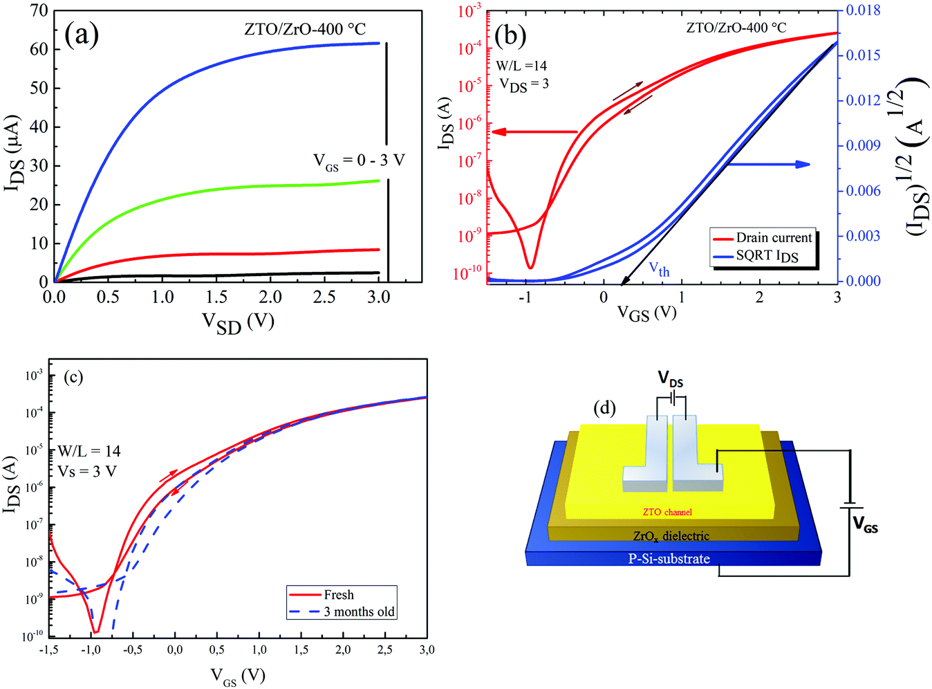 | ||
| Fig. 8 TFT characteristics of ZTO-350/ZrOx-400 devices. (a) Output, and (b) transfer performance; while (c) transfer characteristic of both the freshly made device and the performance after 3 months shelf-life, and the schematic representation of the device structure is shown in (d). | ||
In our case, the clockwise hysteresis was estimated to be −0.1 V, which means that electron trapping occurred during forward sweeping. During the reverse gate voltage sweeping, these states remain filled until the trapped electrons were thermally de-trapped.3 Moreover, Dit is very important for device stability and charge carrier mobility, which was estimated to be 5.7 × 1012 cm−2 for the ZTO/ZrOx TFT. These results show that we obtained a good interface between the ZrOx gate dielectric and the ZTO channel layer. Also, despite being larger than that using SiO2 as the dielectric, the Dit value is comparable to the reported values for solution-processed ZrOx TFTs (1 × 1012 cm−2),8,38 and much lower than that for sputtered TFT devices.40 The improved performance is believed to have originated from the thin and amorphous structure of the ZrOx gate dielectric, providing a smooth interface between the ZrOx dielectric and ZTO semiconductor layer.
The aging stability of the fabricated ZTO/ZrOx TFT device was accessed by re-measuring its performance after 3 months of storage without encapsulation or any specific storage conditions (Fig. 8c). The device showed excellent stability with time and no significant changes in its electrical performance was observed, indicating it demonstrates an effective performance towards cost-effective and low operation voltage solution-based oxide electronics. This may be as a result of the slow sensitivity of the active ZTO layer to native contaminants such as dust and moisture, which have a tendency of increasing the surface energy of semiconductor materials. Moreover, the degradation of the active layer of metal oxide-based TFTs is mostly due their sensitivity to surface adsorbates such as H2O molecules and humidity, which act as trap sites for mobile carriers, and therefore cause depletion of the active layer material.41 Another reason for the shelf-life stability of the device can be due to the in situ deposition of the ZTO layer at high temperature, which led to the formation of a ZTO film with less defects, surface adsorbed species, and organic contaminants. Riedl et al.41 demonstrated that in situ annealing can also be used to improve the stress stability of ALD-processed ZTO-based TFTs.
4. Conclusions
In summary, we successfully reported the solution processing of ZrOx thin films via a low-cost ultrasonic spray pyrolysis method and explored their applicability as a gate dielectric layer in TFTs. The fabricated ZrOx films were uniform, smooth, amorphous, and optically transparent with an Eg value of 5.35 eV. The ZrOx film exhibited a relative permittivity value of 22.7 (50 Hz) and leakage current of 3.56 × 10⁻⁶ A cm−2 at a bias of 1 V. The optimized ZTO/SiO2 TFTs annealed at 350 °C exhibited excellent electrical performances, including a saturation mobility of 0.5 cm2 V−1 s−1, a high Ion/Ioff value of 108, a threshold voltage of 1.32 V, and a small sub-threshold swing value of 0.76 V dec−1. The SiO2 gate dielectric was replaced by the sprayed-deposited ZrOx dielectric to achieve a cost-effective and fully solution-processed device. The ZTO/ZrOx TFTs exhibited a low operation voltage of 3 V with optimized performances, including a high saturation mobility of 4.6 cm2 V−1 s−1, a low threshold voltage of 0.03 V, appreciable Ion/Ioff current ratio of 106, and a small sub-threshold swing of 0.25 V dec−1. These results demonstrate that the use of a very simple technique, such as both ultrasonic spray pyrolysis and spin coating for the sequential deposition of high-κ gate dielectrics and metal oxide semiconductors represents a significant step towards the development of low-cost, large-area oxide TFTs.Conflicts of interest
There are no conflicts to declare.Acknowledgements
This study was financially supported by the Estonian Ministry of Education and Research project IUT194; and by Portuguese National Funds through FCT – Portuguese Foundation for Science and Technology, Reference UID/CTM/50025/2019 and FCT/MCTES; and by the European Union through the European Regional Development Fund project TK141 “Advanced materials and high-technology devices for energy recuperation systems”; and European Institute of Innovation and Technology (EIT RawMaterials, Horizon 2020) Supersmart, Scale-Up of Printed Electronics, Grant Agreement 17161. A. T. Oluwabi acknowledges Archimedes Foundation for financing the study mobility program, through the “DoRa Plus Action 1”, E. Carlos acknowledges FCT/MCTES for a doctoral grant (Grant SFRH/BD/116047/2016). Authors acknowledge Dr V. Mikli of Taltech for SEM measurement, J. V. Pinto, Ana Pimentel, and T. Sequeira of CENIMAT for the XRD, TG/DSC, and AFM measurements respectively.References
- G. X. Liu, A. Liu, F. K. Shan, Y. Meng, B. C. Shin, E. Fortunato and R. Martins, High-performance fully amorphous bilayer metal–oxide thin film transistors using ultra-thin solution-processed ZrOx dielectric, J. Appl. Phys. Lett., 2014, 105(11), 113509 CrossRef.
- P. Barquinha, R. Martins, L. Pereira and E. Fortunato, Transparent oxide electronics, United Kingdom, John Wiley and Sons, 2012 Search PubMed.
- L. Zhu, G. He, J. Lv, E. Fortunato and R. Martins, Fully solution-induced high-performance indium oxide thin film transistors with ZrOx high-κ gate dielectrics, RSC Adv., 2018, 8, 16788 RSC.
- Y. Duan, F. Sun, Y. Yang, P. Chen, D. Yang, Y. Duan and X. Wang, Thin-Film Barrier Performance of Zirconium Oxide Using the Low-Temperature Atomic Layer Deposition Method, ACS Appl. Mater. Interfaces, 2014, 6, 3799–3804 CrossRef CAS PubMed.
- A. Liu, G. X. Liu, H. H. Zhu, F. Xu, E. Fortunato, R. Martins and F. K. Shan, Eco-friendly, solution-processed In–W–O thin films and their applications in low-voltage, high-performance transistors, ACS Appl. Mater. Interfaces, 2014, 6, 17364 CrossRef CAS PubMed.
- M. Hirose, M. Koh, W. Mizubayashi, H. Murakami, K. Shibahara and S. Miyazaki, Fundamental limit of gate oxide thickness scaling in advanced MOSFETs, Semicond. Sci. Technol., 2000, 15, 485–490 CrossRef CAS.
- X. Donga, G. Xia, Q. Zhang, L. Li, H. Gong, J. Bi and S. Wang, Room-temperature UV-ozone assisted solution process for zirconium oxide films with high dielectric properties, Ceram. Int., 2017, 43, 15205–15213 CrossRef.
- C. Zhu, A. Liu, G. Liu, G. Jiang, Y. Meng, E. Fortunato, R. Martins and F. Shan, Low-temperature, nontoxic water-induced high-κ zirconium oxide dielectrics for low-voltage, high-performance oxide thin-film transistors, J. Mater. Chem. C, 2016, 4, 10715 RSC.
- G. Adamopoulos, S. Thomas, P. H. Wöbkenberg, D. D. C. Bradley, M. A. McLachlan and T. D. Anthopoulos, High-Mobility Low-Voltage ZnO and Li-Doped ZnO Transistors Based on ZrO2 High-k Dielectric Grown by Spray Pyrolysis in Ambient Air, Adv. Mater., 2011, 23, 1894–1898 CrossRef CAS PubMed.
- S. Clima, G. Pourtois, A. Hardy, S. Van Elshocht, M. K. Van Bael, S. De Gendt, D. J. Wouters, M. Heyns and J. A. Kittl, Dielectric Response of Ta2O5, Nb2O5, and NbTaO5 from first principles investigations, J. Electrochem. Soc., 2010, 157, G20–G25 CrossRef CAS.
- P. Barquinha, L. Pereira, G. Goncalves, R. Martins, D. Kuscer, M. Kosec and E. Fortunato, Performance and Stability of Low Temperature Transparent Thin-Film Transistors Using Amoorphous Multicomponent Dielectrics, J. Electrochem. Soc., 2009, 156(11), H824–H831 CrossRef CAS.
- J. Tardy, M. Erouel, A. L. Deman, A. Gagnaire, V. Teodorescu, M. G. Blanchin, B. Canut, A. Barau and M. Zaharescu, Organic Thin Film Transistors With HFO2 high-κ Gate Dielectric Grown By Anodic Oxidation Or Deposited By Sol–Gel, Microelectron. Reliab., 2007, vol. 47, 372–377 CrossRef.
- E. Carlos, R. Branquinho, A. Kiazadeh, J. Martins, P. Barquinha, R. Martins and E. Fortunato, Boosting Electrical Performance of high-κ Nanomultilayer Dielectrics and Electronic Devices by Combining Solution Combustion Synthesis and UV Irradiation, ACS Appl. Mater. Interfaces, 2017, 9, 40428–40437 CrossRef CAS PubMed.
- E. Carlos, R. Branquinho, A. Kiazadeh, P. Barquinha, R. Martins and E. Fortunato, UV-mediated photochemical treatment for low-temperature oxide based thin film transistor, ACS Appl. Mater. Interfaces, 2016, 8(45), 31100–31108 CrossRef CAS PubMed.
- D. Panda and T.-Y. Tseng, Growth, dielectric properties, and memory device applications applications of ZrO2 thin films, Thin Solid Films, 2013, 531, 1–20 CrossRef CAS.
- K. Kukli, M. Ritala and M. Leskelä, Low-temperature deposition of zirconium oxide based nanocrystalline films by alternate supply of Zr[OC(CH3)3]4 and H2O, Chem. Vap. Deposition, 2000, 6(6), 297–302 CrossRef CAS.
- A. T. Oluwabi, I. Oja Acik, A. Katerski, A. Mere and M. Krunks, Structural and electrical characterisation of high-κ ZrO2 thin films deposited by chemical spray pyrolysis method, Thin Solid Films, 2018, 662, 129–136 CrossRef CAS.
- A. Juma, I. Oja Acik, A. T. Oluwabi, A. Mere, V. Mikli, M. Danilson and M. Krunks, Zirconium doped TiO2 thin films deposited by chemical spray pyrolysis, Appl. Surf. Sci., 2016, 387, 539–545 CrossRef CAS.
- B. Wang, W. Huang, L. Chi, M. Al-Hashimi and T. J. Marks, high-κ Gate Dielectrics for Emerging Flexible and Stretchable Electronics, Chem. Rev., 2018, 118(11), 5690–5754 CrossRef CAS PubMed.
- A. T. Oluwabi, A. Juma, I. Oja-Acik, A. Katerski, A. Mere and M. Krunks, Effect of Zr doping on the structural and electrical properties of spray deposited TiO2 thin films, Proc. Est. Acad. Sci., 2018, 67(2), 147–157 CrossRef.
- A. Ortiz, J. C. Alonso and E. Haro-Poniatowsk, Spray deposition and characterization of zirconium–oxide, J. Electron. Mater., 2005, 34(2), 150–155 CrossRef CAS.
- B. Wang, X. Yu, P. Guo, W. Huang, L. Zeng, N. Zhou, L. Chi, M. J. Bedzyk, R. P. H. Chang, T. J. Marks and A. Facchetti, Solution-Processed All-Oxide Transparent High-Performance Transistors Fabricated by Spray-Combustion Synthesis, Adv. Electron. Mater., 2016, 2, 1500427 CrossRef.
- J. Robertson and B. Falabretti, Band Offsets of High K Gate Oxides on High Mobility Semiconductors, Mater. Sci. Eng., B, 2006, 135, 267–271 CrossRef CAS.
- H. J. Kwon, J. Jang and C. P. Grigoropoulos, Laser direct writing process for making electrodes and high-κ sol–gel ZrO2 for boosting performances of MoS2 transistors, ACS Appl. Mater. Interfaces, 2016, 8, 9314–9318 CrossRef CAS PubMed.
- W. He, W. Xu, Q. Peng, C. Liu, G. Zhou, S. Wu, M. Zeng, Z. Zhang, J. Gao and X. Gao, Surface modification on solution processable ZrO2 high-κ dielectrics for low voltage operations of organic thin film transistors, J. Phys. Chem. C, 2016, 120, 9949–9957 CrossRef CAS.
- S. J. Kim, D. H. Yoon, Y. S. Rim and H. J. Kim, Low-Temperature Solution-Processed ZrO2 Gate Insulators for Thin-Film Transistors Using High-Pressure Annealing, Electrochem. Solid-State Lett., 2011, 14(11), E35–E37 CrossRef CAS.
- K. Nomura, H. Ohta, A. Takagi, T. Kamiya, M. Hirano and H. Hosono, Room-temperature fabrication of transparent flexible thin-film transistors using amorphous oxide semiconductors, Nature, 2004, 432, 488–492 CrossRef CAS PubMed.
- S. Sanctis, N. Koslowski, R. Hoffmann, C. Guhl, E. Erdem, S. Weber and J. J. Schneider, Toward an Understanding of Thin-Film Transistor Performance in Solution-Processed Amorphous Zinc Tin Oxide (ZTO) Thin Films, ACS Appl. Mater. Interfaces, 2017, 9, 21328–21337 CrossRef CAS PubMed.
- P. K. Nayak, J. V. Pinto, G. Gonçalves, R. Martins and E. Fortunato, Environmental, optical, and electrical stability study of solution-processed zinc-tin-oxide thin film transistors, J. Disp. Technol., 2011, 7, 640 CAS.
- S. Jeong, Y. Jeong and J. Moon, Solution-processed zinc tin oxide semiconductor for thin-film transistors, J. Phys. Chem. C, 2008, 112, 11082–11085 CrossRef CAS.
- D. Salgueiro, A. Kiazadeh, R. Branquinho, L. Santos, P. Barquinha, R. Martins and E. Fortunato, Solution based zinc tin oxide TFTs: the dual role of the organic solvent, J. Phys. D: Appl. Phys., 2017, 50, 065106 CrossRef.
- G. Adamopoulos, A. Bashir, P. H. Wöbkenberg, D. D. Bradley and T. D. Anthopoulos, High-Mobility Low-Voltage ZnO and Li-Doped ZnO Transistors Based on ZrO2 High-k Dielectric Grown by Spray Pyrolysis in Ambient Air, Appl. Phys. Lett., 2009, 95, 133507 CrossRef.
- J. Jang, R. Kitsomboonloha, S. L. Swisher, E. S. Park, H. Kang and V. Subramanian, Transparent High-Performance Thin Film Transistors from Solution-Processed SnO2/ZrO2 Gel-like Precursors, Adv. Mater., 2013, 25, 1042–1047 CrossRef CAS PubMed.
- C.-G. Lee, S. Dutta and A. Dodabalapur, Solution-Processed ZTO TFTs With Recessed Gate and Low Operating Voltage, IEEE Electron Device Lett., 2010, 31(12), 1410–1412 CAS.
- I. Oja Acik, J. Madarász, M. Krunks, K. Tonsuaadu, G. Pokol and L. Niinistö, Titanium(IV) acetylacetonate xerogels for processing titania films: A thermoanalytical study, J. Therm. Anal. Calorim., 2009, 97(1), 39–45 CrossRef.
- M. Krunks, I. Oja Acik, K. Tõnsuaadu, M. Es-Souni, M. Gruselle and L. Niinistö, Thermonalitical study of acetylacetonate-modified titinium(IV) isopropoxide as a precursor for TiO2 films, J. Therm. Anal. Calorim., 2005, 80, 483–488 CrossRef CAS.
- J. I. Pankove, Optical Process in Semiconductors, Prentice-Hall, Englewood Cliffs, N.J., 1971, p. 422 Search PubMed.
- T.-J. Ha and A. Dodabalapur, Photo stability of solution-processed low-voltage high mobility zinc-tin-oxide/ZrO2 thin-film transistors for transparent display applications, Appl. Phys. Lett., 2013, 102, 123506 CrossRef.
- K. Okamura, B. Nasr, R. A. Brand and H. Hahn, Solution-processed oxide semiconductor SnO in p-channel thin-film transistors, J. Mater. Chem., 2012, 22, 4607–4610 RSC.
- J. Li, F. Zhou, H. P. Lin, W. Q. Zhu, J. H. Zhang, X. Y. Jiang and Z. L. Zhang, SiOx interlayer to enhance the performance of InGaZnO TFT with AlOx gate insulator, Curr. Appl. Phys., 2012, 12, 1288–1291 CrossRef.
- M. Fakhri, P. Görrn and T. Riedl, Stability and encapsulation of metal–oxide based TFTs, in Active-Matrix Flat panel Displays and Devices (AM-FPD), 2013.
Footnote |
| † Electronic supplementary information (ESI) available. See DOI: 10.1039/c9tc05127a |
| This journal is © The Royal Society of Chemistry 2020 |