Improved switching characteristics of p-type tin monoxide field-effect transistors through Schottky energy barrier engineering†
Received
8th August 2019
, Accepted 15th November 2019
First published on 15th November 2019
Abstract
A low on–off current modulation ratio (ION/OFF) in p-type tin monoxide (SnO) field-effect transistors (FETs) is a critical bottleneck hampering their widespread application to transparent complementary metal oxide semiconductors (CMOSs) or monolithic integrated devices. To solve this problem, this study focuses on the source/drain (S/D) contact region. Also, a new perspective on the origin of the high off-current in SnO FETs, an electron injection from the drain electrode into the channel by Fermi-level pinning (FLP) at the off-state, is suggested. In this work, a metal–interlayer–semiconductor (MIS) S/D contact structure is adopted to suppress this adverse electron injection. An ultrathin interlayer (IL) of MIS contact alleviates metal-induced gap state (MIGS) penetration which is a primary cause of the severe FLP. A considerable enhancement is achieved by using the MIS contact structure: the off-current value decreased by approximately 20-fold from 5.1 × 10⁻⁸ A to 2.4 × 10⁻⁹ A; the ION/OFF value increased 10-fold from 2.7 × 10² to 2.8 × 10³, which is interpreted by increased MIS contact-mediated electron SBH. This work presents a new approach that can be easily used alongside previously reported methods to suppress the off-current, providing enhanced switching capability of p-type SnO FETs using a simple method.
Introduction
Since the invention of n-type amorphous In–Ga–Zn–O (a-IGZO) semiconductors by Hosono and co-workers in 2004, a-IGZO field-effect transistors (FETs) have attracted a tremendous amount of attention because they possess several intriguing properties such as high field-effect mobility (μFE), extremely low off-current, and good visible light transparency despite being fabricated at room temperature.1 Based on these advantages, amorphous oxide semiconductor (AOS) FETs are used in high-end active-matrix liquid crystal displays (AMLCDs) and active-matrix organic light-emitting displays (AMOLEDs) with ultra-high-pixel density and low-power consumption as backplane electronics.2 However, application of AOS has been limited to n-type FETs because p-type oxide semiconductor-based FETs have comparatively inferior electrical properties.3,4
In p-type metal oxide semiconductors, the valence band (VB) edge acts as a hole conduction path, which is severely localized due to the O 2p orbitals that have anisotropic and small ionic radius. Therefore, the hole effective mass (mh*) increases, resulting in poor electrical characteristics and limiting the application of p-type oxide semiconductors.5 Owing to this issue, some limited p-type oxide semiconductors on the basis of copper, nickel, and tin have been mainly investigated as an active layer for p-channel FETs.6–16 Among them, tin monoxide (SnO) has been intensively researched because of its isotropic Sn 5s orbitals with large ionic radius that constitute the VB edge, which has a relatively high degree of delocalization allowing for a small mh* and promising p-type characteristics.17 Additionally, SnO has a large direct bandgap (Eg) of ∼2.9 eV, making it an excellent hole conducting candidate for transparent electronics.4,18 However, FETs with these p-type oxide semiconductors including SnO still show an inferior on–off current modulation ratio (ION/OFF) coming from high off-current, which hinders their widespread use as a complementary metal oxide semiconductor (CMOS) inverter for many emerging electronic systems such as hybrid digital/analogue and monolithic three-dimensional devices. Therefore, several researchers have aimed to improve the poor ION/OFF values of p-type SnO FETs through various approaches with the conjecture that the origin of high off-current is (1) existence of Sn4+ causing n-type characteristics,19 (2) segregation of excess Sn,20 and (3) defect states and hole carriers near the surface.21 However, there is still an issue with regard to the origin of the high off-current and low ION/OFF in p-type SnO FETs.
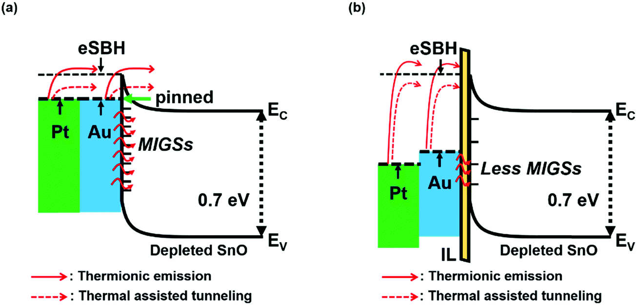
In this study, a novel approach using a metal–interlayer–semiconductor (MIS) contact scheme at the source/drain (S/D) region is proposed to reduce the off-current in SnO FETs. Insertion of an interlayer (IL) prevents the tail of the electron wave function of the metal electrode, which forms metal-induced gap states (MIGSs) in the semiconductor, from penetrating the semiconductor effectively.22 Fermi-level pinning (FLP) at metal/semiconductor interfaces is caused by several factors such as uncontrolled chemical reactions, native point defects, interface trap states (Dit), and MIGSs.23–26 Note that FLP mostly results from the MIGSs via the metal–semiconductor (MS) contact in semiconductors with narrow Eg.27 Therefore, this MIS contact scheme has been adopted in several material-based devices primarily characterized by narrow Eg semiconductors such as germanium metal–oxide–semiconductor field effect transistors (Ge MOSFETs)28–35 and two-dimensional dichalcogenides (TMDs).36–39 Likewise, MIGS-induced FLP is expected to be severe in SnO FETs due to its narrow indirect Eg of 0.7 eV, unlike other AOSs such as IGZO or zinc oxide (ZnO).4 Thus, it is clear that FLP can be mitigated using the MIS contact in SnO FETs, allowing for easier control of the Schottky barrier height (SBH). The design of this study is as follows. MIGS-induced FLP in FETs using the MS S/D contact permits the penetration of electrons from the drain electrode through either thermionic emission or thermally assisted tunneling in the off-state, as depicted in Fig. 1a. In contrast, insertion of a wide Eg insulator such as Al2O3 can reduce the effect of the MIGSs.40 Therefore, the insertion of an ultrathin Al2O3 IL mitigates FLP and effectively raises the eSBH, leading to a substantial decrease in the off-current (Fig. 1b). The present work verifies that such FLP is severe in SnO FETs using the MS contact and provides a new possible origin of the high off-current by adopting an MIS contact with Au (∼5.2 eV) and Pt (∼5.5 eV).
 |
| | Fig. 1 Energy band diagrams of a metal/depleted channel layer in the off-state: (a) FLP by MIGSs with high density, and electron injection from the Au or Pt electrode into SnO at the MS contact. (b) FLP alleviation and controllability of the SBH depending on the metal electrode through the MIS contact. | |
Experimental method
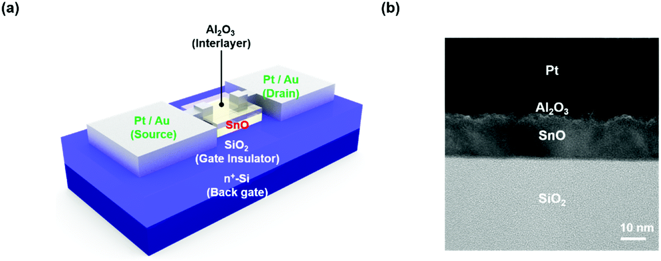
FETs with a 20 nm-thick SnO channel were fabricated with top contacted S/D electrodes on thermally oxidized SiO2 (100 nm)/heavily doped silicon substrates, where the conducting silicon substrate acts as a gate electrode. The SnO channel layer was deposited using reactive sputtering with a Sn target (99.999%). After deposition, the SnO thin-films were annealed at 200 °C for 3 hours in ambient air. Then, metal S/D electrodes were deposited using an evaporator. The channel and S/D patterning was performed using a metal shadow mask. The channel width (W) and length (L) of the fabricated FETs were 100 μm and 150 μm, respectively. In MIS FETs, before deposition of the metal electrodes, an ultrathin Al2O3 IL was deposited between the SnO channel layer and the S/D metal electrode using thermal atomic layer deposition (ALD) at 150 °C. A schematic of a three-dimensional device structure is shown in Fig. 2a. Fig. 2b shows a cross-sectional transmission electron microscopy (XTEM) image of the MIS contact, which clearly indicates the formation of a Pt(Au)/Al2O3/SnO stack under the S/D electrodes.
 |
| | Fig. 2 (a) 3-D structure of MIS FETs. (b) Cross-sectional transmission electron microscopy (XTEM) image at the MIS contact area. | |
Results and discussion
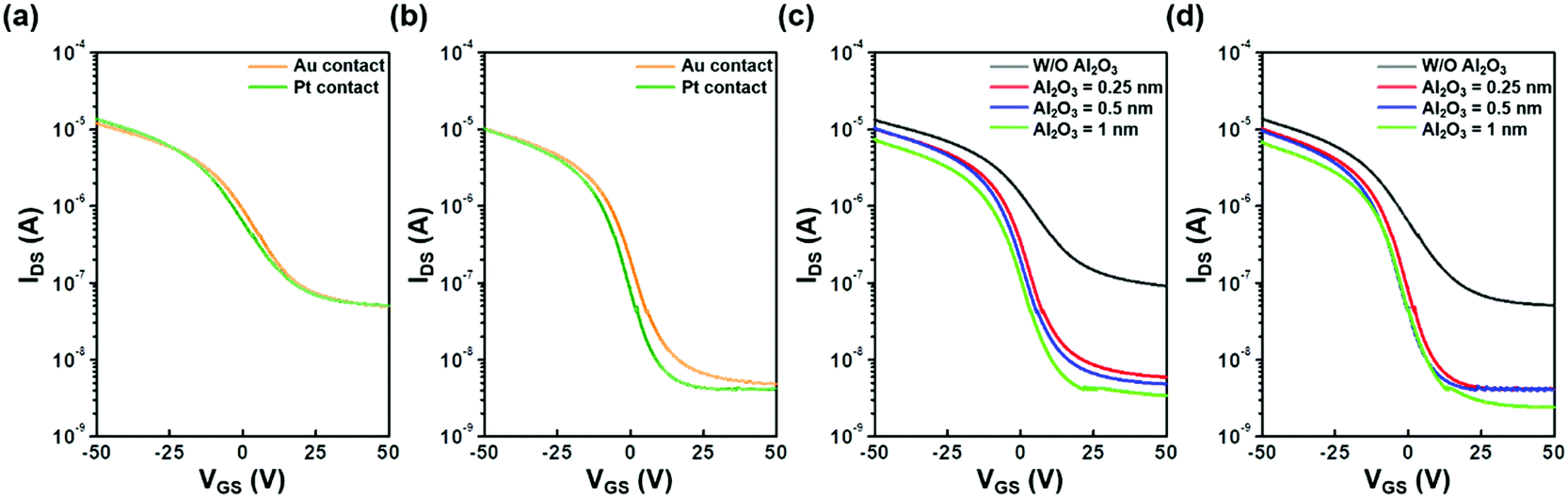
Fig. 3a shows the transfer characteristics of p-type SnO FETs without IL at the S/D contact region (referred to herein as MS FETs). It can be seen that the parasitic leakage current through the gate insulator for all devices is negligible compared to the off-current level of the corresponding transfer characteristics (Fig. S1, ESI†). Regardless of which metal S/D electrode was used, both FETs show almost the same device performances, demonstrating that severe FLP occurs in the MS FETs. This corresponds to the Bardeen limit where the contact energy barrier and carrier conduction are independent of S/D work function. However, in FETs with IL (referred to herein as MIS FETs), substantial reduction in the off-current level is observed for SnO FETs with metal S/D electrodes that have a higher work-function (Fig. 3b). Additionally, MIS FETs exhibit superior transfer characteristics compared to the MS FETs, as shown in Fig. 3a and b. In particular, the off-current of the MIS FETs with a Pt electrode is reduced significantly from 5.1 × 10⁻⁸ A to 2.4 × 10⁻⁹ A.
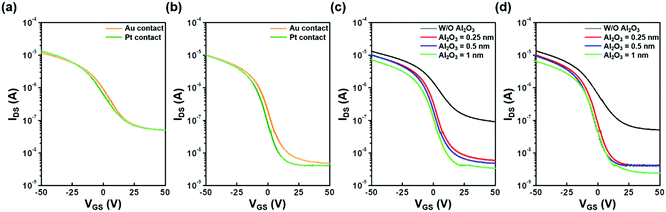 |
| | Fig. 3 Transfer characteristics at VDS = −5.1 V: (a) MS FETs and (b) MIS FETs with 0.5 nm-thick IL. Overall transfer characteristics depending on IL thickness using (c) Au S/D electrode, and (d) Pt S/D electrode. | |
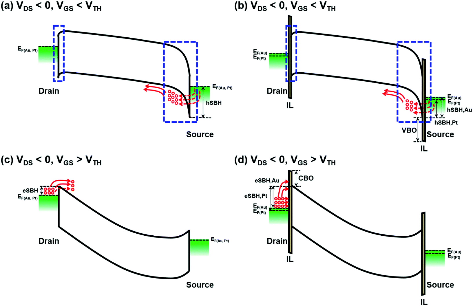
Fig. 3c and d show the transfer characteristics of the MIS SnO FETs with varying Al2O3 IL thickness. As the IL thickness increases, the on-current as well as the off-current for the given FETs are reduced independent of the metal electrode used. The lower positioning of the Fermi-level in the MIS FETs compared to that in MS FETs would favor the facile injection of hole carriers under the on-state conditions, which cannot explain this observation (Fig. 1). The formation of a high valence band offset (VBO, ∼5.4 eV) between the Al2O3 IL and SnO is partially responsible for its lower on-current because high VBO strongly retards the hole injection from the source contact (Fig. 4a and b). Moreover, the hole tunneling probability from the source electrode can decrease with increasing IL thickness (increasing energy barrier strength), thereby leading to the reduction of the on-current. The latter mechanism can be further confirmed by the IL-dependent output characteristics (Fig. 5).
 |
| | Fig. 4 Energy band diagrams representing carrier injection at the on/off state. On-state: (a) MS contact and (b) MIS contact. The blue box represents the hole depletion region at the S/D contact area. Off-state: (c) MS contact and (d) MIS contact. FLP in the MS contact and FLP alleviation in the MIS contact are also described by SBH deviation between the MS contact [(a) and (c)] and the MIS contact [(b) and (d)]. | |
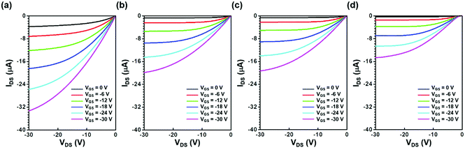 |
| | Fig. 5 Output characteristics of the p-type SnO FETs using a Pt S/D electrode depending on the IL thickness. (a) 0 nm. (b) 0.25 nm. (c) 0.5 nm. (d) 1 nm. | |
The drain current of SnO FETs decreases with increasing IL thickness under the identical VGS and VDS conditions. A quantitative interpretation is given by investigating the contact resistances (RC) of MS and MIS stacks using the circular transmission line method (CTLM) where the geometry of the CTLM pattern is depicted in Fig. S2 (ESI†). The RC values (0.12–0.13 MΩ) for MS stacks with Pt and Au electrodes are comparable to each other. In contrast, the RC values for MIS stacks with 0.5 nm-thick IL increased substantially to 0.47–0.66 MΩ, which is attributed to additional resistance from the Al2O3 IL. The corresponding RC values for the MS and MIS stacks are summarized in Table S1 (ESI†). The increasing RC value with increasing IL thickness adversely affects the output characteristics of the MIS FETs especially in the low VDS region, as shown in Fig. S3 (ESI†). Note that the linearity of VDSvs. IDS is broken as IL thickness increases, indicating that the current flow for the MIS FETs with thick IL is limited considerably by the S/D contact resistance as well as the channel resistance. It is assumed that the hole Schottky barrier height (hSBH) is lowered through insertion of the IL, which is confirmed later in detail. In light of this result, we expect the on-current to be improved by adopting another IL with a lower VBO than that of Al2O3, as shown in Fig. S4 (ESI†). Several studies on this MIS contact scheme have reported an enhanced device performance achieved by using an IL such as ZnO and titanium oxide (TiO2), which have no conduction band offset (CBO) between the n-type Ge and the IL.29,32,35,36,41
In the case of the off-current, the Fermi-level depinning via the MIS contact structure lowers the position of the Fermi-level, leading to an increased eSBH as shown in Fig. 4c and d. Therefore, the electron injected from the drain electrode to the channel at the off-state is reduced in the MIS SnO FETs. However, the off-current is heavily suppressed, unlike the on-current, resulting in an enhanced ION/OFF. This is due to the large CBO and increased eSBH (Fig. 4c and d). This interpretation is corroborated by the work function-dependent variations of the transfer characteristics: when a higher work function metal (Pt) S/D is used, the electron injection from the S/D electrode to the SnO channel layer decreases, i.e., the reduced off-current flows since the Fermi-level is located at a lower position (Fig. 1). The overall electrical parameters depending on IL thickness are summarized in Table 1.
Table 1 Electrical parameters and hSBHs of MS and MIS FETs with Au and Pt S/D electrodes. ION and IOFF values are defined as IDS at VGS = −50 V and +50 V, respectively, at VDS = −5.1 V
|
|
Au |
Pt |
|
μ
FET [cm2 V−1 s−1] |
I
ON/OFF
|
I
ON [A] |
I
OFF [A] |
hSBH [eV] |
μ
FET [cm2 V−1 s−1] |
I
ON/OFF
|
I
ON [A] |
I
OFF [A] |
hSBH [eV] |
| W/O IL |
2.04 |
2.44 × 10² |
1.34 × 10⁻⁵ |
9.04 × 10⁻⁸ |
0.57 |
2.23 |
2.71 × 10² |
1.36 × 10⁻⁵ |
5.08 × 10⁻⁸ |
0.57 |
| IL = 0.25 nm |
1.73 |
1.74 × 10³ |
1.03 × 10⁻⁵ |
5.85 × 10⁻⁹ |
0.50 |
1.84 |
2.48 × 10³ |
1.02 × 10⁻⁵ |
4.13 × 10⁻⁹ |
0.48 |
| IL = 0.5 nm |
1.71 |
2.16 × 10³ |
1.02 × 10⁻⁵ |
4.76 × 10⁻⁹ |
0.43 |
1.71 |
2.53 × 10³ |
1.02 × 10⁻⁵ |
4.02 × 10⁻⁹ |
0.40 |
| IL = 1 nm |
1.31 |
2.24 × 10³ |
7.62 × 10⁻⁶ |
3.40 × 10⁻⁹ |
0.25 |
1.23 |
2.82 × 10³ |
6.77 × 10⁻⁶ |
2.38 × 10⁻⁹ |
0.22 |
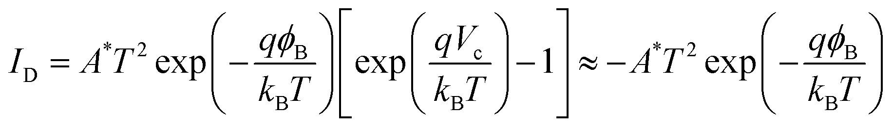
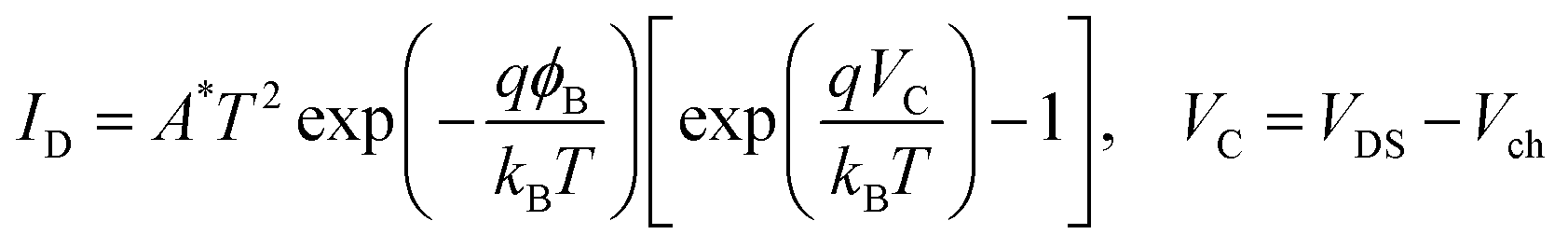
Using the I–V characteristics obtained in this device structure, the SBH values depending on the IL thickness are obtained, demonstrating severe FLP in the MS contact as well as depinning through the MIS contact.37–39,42 It was shown that the SBHs extracted by this method are highly reliable, comparable to those extracted by the Arrhenius plot and simulation.42 Since then, this extraction method has been widely adopted by many groups to extract the SBH value in both MS and MIS contact limited transistors.20–22 The thermionic emission in the MS contact can be generally described as follows:43
| | 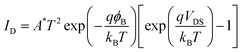 | (1) |
where
ID is the drain current,
A* is the effective Richardson constant,
T is the temperature,
q is the electronic charge,
kB is the Boltzmann constant,
ϕB is the effective SBH, and
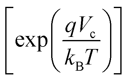
VDS is the drain to source bias. However, some portion of the
VDS is applied to the channel layer, resulting in the reduction of the voltage applied at the contacted S/D region. Thus,
eqn (1) should be modified by
eqn (2), which takes the voltage division along the S/D junction and channel area into consideration:
44| | 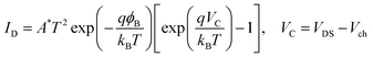 | (2) |
where
VC is the voltage biased on the contact area and
Vch is the voltage dropped off across the channel. Both the total resistance (
RT) and contact resistance (
RC) were calculated to estimate the
VDS portion into
VC and
Vch through the device structure. The
RT value at
VGS =
VFB was estimated by using the slope of the output curve, which was found to be ∼1.6 and ∼2.5 MΩ for the MS and 0.5 nm-thick MIS contact, respectively.
45 Also, the
RC values for the MS and MIS devices were calculated by CTLM, which are described in the ESI.
† The
RC values for the MS contacts (M = Pt and Au) were 0.13 MΩ and 0.12 MΩ, respectively, whereas those of the MIS contacts (M = Pt and Au) with a 0.5 nm-thick Al
2O
3 layer were 0.47 MΩ and 0.66 MΩ, respectively. Since the ratios of
RC to
RT are ∼0.08, and ∼0.25 for the MS and 0.5 nm-thick MIS contact, respectively, it can be known that the corresponding
VC values are approximately −0.42, and −1.29 V. It makes the exponential term

negligible because the absolute
VC value is much larger than
kBT/
q (∼0.0259 V) as shown in
eqn (3):
| | 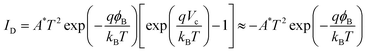 | (3) |
The obtained SBHs are hardly affected by the approximation because the voltage drop across the channel has a negligible effect on the extraction of the SBH.
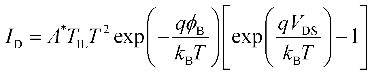
When evaluating thermionic emission in the MIS contact, unlike MS contact, tunneling probability through the IL should be considered as follows:43
| |  | (4) |
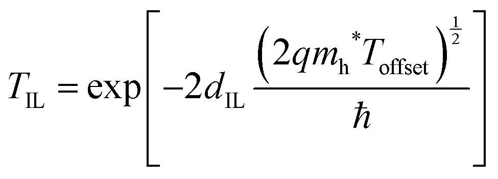
This equation assumes that the IL is so thin that the applied VDS in the IL is negligible. In eqn (4), TIL is the tunneling probability of the hole and is given by the following equation:43
| | 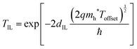 | (5) |
where
dIL is the thickness of the IL,
mh* is the hole effective mass,
ħ is Dirac's constant, and
Toffset is the value of the VBO. The variations in the SBH as a function of
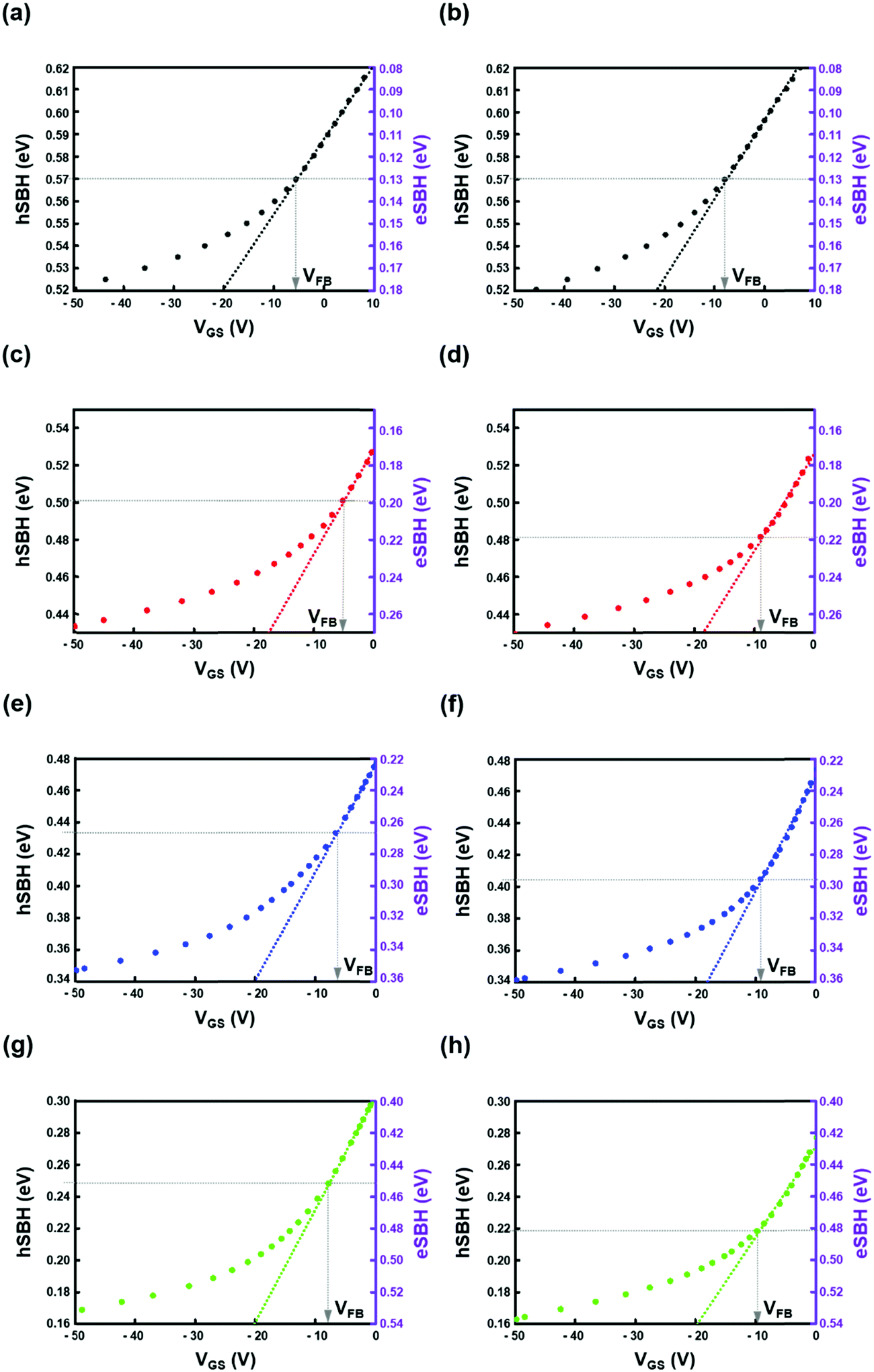
VGS for the MS and MIS devices can be seen in
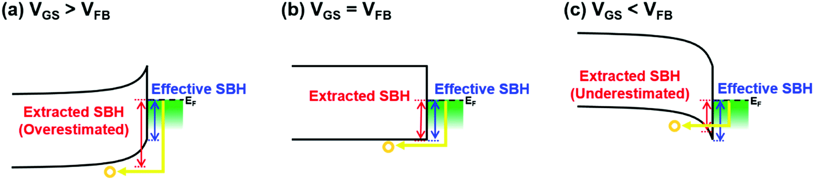
Fig. 6. This
VGS dependent hSBH behavior can be understood by considering the energy band diagram in
Fig. 7, which describes the existing current components including thermionic emission and thermally assisted tunneling under different three
VGS conditions: above flat band (
VFB), at
VFB, and below
VFB. When
VGS is higher than
VFB, the contribution of the tunneling current by the hole carrier to the overall current becomes negligible; this is because the
VGS-induced downward band bending prevents the holes from tunneling into the bandgap, as shown in
Fig. 7a. Thus, hole injection through the thermionic emission mechanism becomes predominant in the observed current flow. The linear relation between hSBH and
VGS in this region is anticipated because (i) the SBH value is extracted on the basis of the thermionic equation and (ii) any change in
VGS directly translates into a corresponding change in the hSBH. The analytical expression can be found in the ESI,
† which explains the linear relation between the
VGS and SBH under the gate voltage region:
VGS >
VFB. The decreasing
VGS causes the upward band bending but the obtained SBHs are overestimated at
VGS >
VFB for the given SnO transistor (
Fig. 7a). On the other hand, thermally assisted tunneling and thermionic emission contribute to the current flow with
VGS <
VFB, as depicted in
Fig. 7c. This leads to a deviation from linearity (see
Fig. 6) and underestimated hSBH, as shown in
Fig. 7c. Therefore, the hSBHs must be obtained at
VGS =
VFB (
Fig. 7b).
 |
| | Fig. 6 Hole/electron SBH dependence on VGS. (a) MS, (c) 0.25 nm-thick, (e) 0.5 nm-thick, and (g) 1 nm-thick MIS contact with a Au S/D electrode. (b) MS, (d) 0.25 nm-thick, (f) 0.5 nm-thick, and (h) MIS contact with a Pt S/D electrode. | |
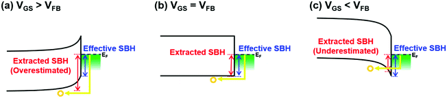 |
| | Fig. 7 Band diagram depending on VGS, and the schematic of the carrier injection and extracted SBH. (a) VGS > VFB. (b) VGS = VFB. (c) VGS < VFB. | |
The hSBHs are obtained as 0.57 eV in the MS FETs regardless of the metal electrode as shown in Fig. 6a and b, indicating that a pinning point, charge neutrality level (ECNL), in SnO is located ∼0.13 eV below the conduction band minimum (CBM). This result verifies the existence of a strong FLP phenomenon at the interface between metal electrodes (Au and Pt) and SnO. Note that the location of ECNL of SnO is identified in this study for the first time. Interestingly, the MIS contact has a smaller hSBH than the MS contact, where the hSBH decreases with increasing IL thickness. The hSBH for the MIS contact (1 nm-thick IL) with Au metal is reduced from 0.50 eV (0.25 nm-thick IL) to 0.25 eV, indicating Fermi-level depinning through the MIS contact. In addition, the hSBH is lower in the MIS FETs using the metal with a higher work function, as shown in Fig. 6c–h, indicating that the MIS FETs with a Pt S/D electrode have a larger eSBH. These results support that the off-current in the MIS FETs with Pt is lower than that with Au, as illustrated in Fig. 4d. The overall hSBH values are also summarized in Table 1. It should also be noted that the uncertainty in SBH values can arise for the MIS contact with the thickest (1 nm) Al2O3 IL because the portion of VDS applied in the IL can be significant. Thus, the fitting based on eqn (4) assuming negligible VDS in the IL becomes inaccurate. We observe the deviations in hSBHs (ΔhSBH) between Au and Pt electrodes at the same IL thickness: these differences (ΔhSBH) are ∼0.02 eV, 0.03 eV, and 0.03 eV for the samples with an IL thickness of 0.25 nm, 0.5 nm, and 1.0 nm, respectively. The observed deviations are also consistent with the alleviation of the FLP in the MIS contact scheme. Moreover, we infer that the SBH of the device with the 1 nm-thick IL is almost the same as that of the 0.5 nm-thick IL due to these deviations. This is because the numerical differences of ΔhSBH between 0.5 nm and 1 nm are the same (∼0.03 eV), which means that the amount of FLP alleviation for the two cases is the same. This SBH deviation is coherent with the enhanced electrical performance (high on–off ratio) when employing a Pt electrode rather than an Au electrode, as already discussed in Fig. 3b.
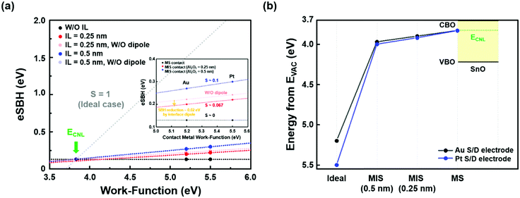
Fig. 8 summarizes the degree of FLP in both MS and MIS contacts. The SBHs of the MS and MIS contacts as a function of the work-function of metal electrodes are plotted in Fig. 8a. The S parameter (pinning factor), which is a measure of the FLP degree, is specified for each contact scheme; ‘S = 0’ and ‘S = 1’ indicate the Fermi-level to be completely pinned and unpinned, respectively.46 For the MS contact, the S parameter is almost zero, indicating strong FLP and uncontrollability of the SBH regardless of the metal work-function, which is well-known as the Bardeen limit. However, the S parameter is ∼0.067 for the MIS contact with a 0.25 nm-thick IL and increases to ∼0.1 for MIS contacts with 0.5 nm- and 1 nm-thick ILs. Here, the difference in areal oxygen density (AOD) between IL and SnO may result in the diffusion of oxygen atoms, which introduces the atomic-scale interfacial dipole.35 However, it was confirmed that the dipole-induced potential does not have a significant effect on the determination of SBHs in this work: the reduction in SBHs by the dipole-induced potential was ∼0.02 eV and ∼0 eV in MIS contacts with 0.25 and 0.5 nm-thick ILs, respectively. Extraction of the S parameter is explained in the ESI.† This result supports the fact that the strong FLP is partially alleviated by reduction of MIGSs at SnO interfaces. Fig. 8b displays the alignment of the Fermi-level location in both MS and MIS contacts with respect to the metal electrodes. As expected, there is a comparable difference between the alignment of the ideal case (S = 1) and that of the MIS contacts presented in this work. This hints that the FLP phenomenon comes from not only MIGSs but also the interfacial trap states even though the MIGS-induced FLP was mainly discussed in this work. Indeed, the SnO surface suffered from various defects such as Sn4+ ions, local vacancies and antisites, which also hinder perfect alleviation of FLP.47 Thus, it would be beneficial in FLP alleviation to use the chemically stable IL in order to avoid any deterioration of interface states by oxygen stoichiometry. Therefore, further investigation such as surface healing or passivation techniques in conjunction with the IL insertion is needed to achieve a more controllable SBH in the MIS contact scheme, which may be helpful to obtain acceptable electrical performance of the p-type SnO FET.
 |
| | Fig. 8 (a) Effective eSBH of MS and MIS contacts (0.25 nm, and 0.5 nm) for the different metal work-functions (Au and Pt). The slope of each line indicates the S parameter. The inset shows the magnified portion of (a) where metal work-function values range from 5.0 eV to 5.6 eV. (b) Band alignment of different metals (Au and Pt) in contact with SnO for the MS contact, MIS contacts (0.25 nm, 0.5 nm), and ideal contact. | |
Conclusions
In conclusion, the impact of FLP between the metal electrode and p-type semiconducting SnO channel on the device performance of SnO FETs was examined. The MS SnO FETs suffered from strong pinning of the Fermi-level at approximately 0.13 eV below the CB edge independent of the metal electrodes, which resulted in the low on/off modulation capability of the resulting MS SnO FET. This strong FLP phenomenon is effectively alleviated through the MIS contact scheme. Thus, the off-current of the MIS SnO FET is reduced from 5.1 × 10⁻⁸ A (MS device) to 2.4 × 10⁻⁹ A due to the increased eSBH, leading to an enhanced ION/OFF from 2.7 × 10² to 2.8 × 10³. A new insight exploiting the Fermi-level depinning via the MIS contact scheme can be implemented in conjunction with other off-current reduction methods. Also, the MIS contact structure can be adopted into other p-type oxide (Cu2O, NiO, etc.) FETs, enabling the use of a transparent CMOS device into versatile emerging devices such as monolithic three-dimensional devices and hybrid logic/memory devices.
Conflicts of interest
There are no conflicts to declare.
Acknowledgements
This work was supported by the Samsung Research Funding Center for Future Technology through Samsung Electronics.
Notes and references
- K. Nomura, H. Ohta, A. Takagi, T. Kamiya, M. Hirano and H. Hosono, Nature, 2004, 432, 488 CrossRef CAS.
- J. F. Wager and R. Hoffman, IEEE Spectrum, 2011, 48, 42 Search PubMed.
- E. Fortunato, R. Barros, P. Barquinha, V. Figueiredo, S.-H. K. Park, C.-S. Hwang and R. Martins, Appl. Phys. Lett., 2010, 97, 052105 CrossRef.
- Y. Ogo, H. Hiramatsu, K. Nomura, H. Yanagi, T. Kamiya, M. Hirano and H. Hosono, Appl. Phys. Lett., 2008, 93, 032113 CrossRef.
- H. Kawazoe, M. Yasukawa, H. Hyodo, M. Kurita, H. Yanagi and H. Hosono, Nature, 1997, 389, 939–942 CrossRef CAS.
- T. Mine, H. Yanagi, K. Nomura, T. Kamiya, M. Hirano and H. Hosono, Thin Solid Films, 2008, 516, 5790–5794 CrossRef CAS.
- S. Han and A. J. Flewitt, IEEE Electron Device Lett., 2017, 38, 1394–1397 CAS.
- S. J. Lee, Y. Jang, H. J. Kim, E. S. Hwang, S. M. Jeon, J. S. Kim, T. Moon, K.-T. Jang, Y.-C. Joo, D.-Y. Cho and C. S. Hwang, ACS Appl. Mater. Interfaces, 2018, 10, 3810–3821 CrossRef CAS.
- A. Liu, H. Zhu and Y.-Y. Noh, ACS Appl. Mater. Interfaces, 2019, 11, 33157–33164 CrossRef CAS.
- F. Shan, A. Liu, H. Zhu, W. Kong, J. Liu, B. Shin, E. Fortunato, R. Martins and G. Liu, J. Mater. Chem. C, 2016, 4, 9438–9444 RSC.
- T. Lin, X. Li and J. Jang, Appl. Phys. Lett., 2016, 108, 233503 CrossRef.
- J. Yang, B. Wang, Y. Zhang, X. Ding and J. Zhang, J. Mater. Chem. C, 2018, 6, 12584 RSC.
- S. J. Han, S. Kim, J. Ahn, J. K. Jeong, H. Yang and H. J. Kim, RSC Adv., 2016, 6, 71757–71766 RSC.
- A. Azmi, J. Lee, T. J. Gim, R. Choi and J. K. Jeong, IEEE Electron Device Lett., 2017, 38, 1543–1546 CAS.
- C. W. Shih, A. Chin, C. F. Lu and W. F. Su, Sci. Rep., 2018, 8, 889 CrossRef.
- T. Kim, B. Yoo, Y. Youn, M. Lee, A. Song, K.-B. Chung, S. Han and J. K. Jeong, ACS Appl. Mater. Interfaces, 2019, 11, 40214–40221 CrossRef CAS.
- A. Togo, F. Oba, I. Tanaka and K. Tatsumi, Phys. Rev. B: Condens. Matter Mater. Phys., 2006, 74, 195128 CrossRef.
- J. A. Caraveo-Frescas, P. K. Nayak, H. A. Al-Jawhari, D. B. Granato, U. Schwingenschlögl and H. N. Alshareef, ACS Nano, 2013, 7, 5160–5167 CrossRef CAS.
- M. P. Hung, J. Genoe, P. Heremans and S. Steudel, Appl. Phys. Lett., 2018, 112, 263502 CrossRef.
- J. B. Varley, A. Schleife, A. Janotti and C. G. Van de Walle, Appl. Phys. Lett., 2013, 103, 082118 CrossRef.
- S.-H. Kim, I. H. Baek, D. H. Kim, J. J. Pyeon, T. M. Chung, S. H. Baek, J.-S. Kim, J. H. Han and S. K. Kim, J. Mater. Chem. C, 2017, 5, 3139–3145 RSC.
- W. Mönch, Rep. Prog. Phys., 1990, 53, 221–278 CrossRef.
- L. J. Brillson, J. Vac. Sci. Technol., A, 2007, 25, 943 CrossRef CAS.
- L. J. Brillson, Y. Dong, F. Tuomisto, B. G. Svensson, A. Y. Kuznetsov, D. Doutt, H. L. Mosbacker, G. Cantwell, J. Zhang, J. J. Song, Z.-Q. Fang and D. C. Look, J. Vac. Sci. Technol., B, 2012, 30, 050801 CrossRef.
- A. Klein, J. Am. Ceram. Soc., 2016, 99, 369–387 CrossRef CAS.
- T. Schultz, S. Vogt, P. Schlupp, H. Wenckstern, N. Koch and M. Grundmann, Phys. Rev. Appl., 2018, 9, 064001 CrossRef CAS.
- T. Nishimura, K. Kita and A. Toriumi, Appl. Phys. Lett., 2007, 91, 123123 CrossRef.
- G.-S. Kim, J.-K. Kim, S.-H. Kim, J. Jo, C. Shin, J.-H. Park, K. C. Saraswat and H.-Y. Yu, IEEE Electron Device Lett., 2014, 35, 1076–1078 CAS.
- S. Dev, N. Remesh, Y. Rawal, P. P. Manik, B. Wood and S. Lodha, Appl. Phys. Lett., 2016, 108, 103507 CrossRef.
- B. Y. Tsui and M. H. Kao, Appl. Phys. Lett., 2013, 103, 032104 CrossRef.
- G.-S. Kim, S.-W. Kim, S.-H. Kim, J. Park, Y. Seo, B. J. Cho, C. Shin, J. H. Shim and H.-Y. Yu, ACS Appl. Mater. Interfaces, 2016, 8, 35419–35425 CrossRef CAS.
- J. Y. J. Lin, A. M. Roy and K. C. Saraswat, IEEE Electron Device Lett., 2012, 33(11), 1541–1543 CAS.
- A. Agrawal, N. Shukla, K. Ahmed and S. Datta, Appl. Phys. Lett., 2012, 101(4), 042108 CrossRef.
- S.-W. Kim, S.-H. Kim, G.-S. Kim, C.-H. Choi, R. Choi and H.-Y. Yu, ACS Appl. Mater. Interfaces, 2016, 8, 35614–35620 CrossRef CAS.
- G.-S. Kim, S.-W. Kim, S.-H. Kim, J. Park, Y. Seo, B. J. Cho, C. Shin, J. H. Shim and H.-Y. Yu, ACS Appl. Mater. Interfaces, 2016, 8, 35419–35425 CrossRef CAS.
- S. Das, H. Y. Chen, A. V. Penumatcha and J. Appenzeller, Nano Lett., 2013, 13, 100–105 CrossRef CAS.
- S. Lee, A. Tang, S. Aloni and H. S. P. Wong, Nano Lett., 2016, 16, 276–281 CrossRef CAS PubMed.
- G.-S. Kim, S.-H. Kim, J. Park, K. H. Han, J. Kim and H.-Y. Yu, ACS Nano, 2018, 12, 6292–6300 CrossRef CAS.
- S.-H. Kim, G.-S. Kim, J. Park, C. Lee, H. Kim, J. Kim, J. H. Shim and H.-Y. Yu, ACS Appl. Mater. Interfaces, 2018, 10, 26378–26386 CrossRef CAS PubMed.
- R. T. Tung, Appl. Phys. Rev., 2014, 1, 011304 Search PubMed.
- J.-K. Kim, G.-S. Kim, H. Nam, C. Shin, J.-H. Park, J.-K. Kim, B. J. Cho, K. C. Saraswat and H.-Y. Yu, IEEE Electron Device Lett., 2014, 35, 1185–1187 CAS.
- J. Appenzeller, M. Radosavljevic, J. Knoch and P. Avouris, Phys. Rev. Lett., 2004, 92, 048301 CrossRef CAS.
-
D. K. Schroder, Semiconductor Material and Device Characterization, John Wiley & Sons, 2006 Search PubMed.
-
S. D. Brotherton, Introduction to Thin Film Transistors, Springer, 2013 Search PubMed.
-
S. M. Sze and K. K. Ng, Physics of Semiconductor Devices, Wiley, 2006 Search PubMed.
- J. F. Wager and J. Robertson, J. Appl. Phys., 2011, 109, 094501 CrossRef.
- J.-K. Kim, S.-H. Kim, T. Kim and H.-Y. Yu, IEEE Trans. Electron Devices, 2018, 65(11), 4982–4987 CAS.
Footnotes |
| † Electronic supplementary information (ESI) available. See DOI: 10.1039/c9tc04345d |
| ‡ T. Kim and J.-K. Kim contributed to this work equally. |
|
| This journal is © The Royal Society of Chemistry 2020 |
Click here to see how this site uses Cookies. View our privacy policy here. 
 a,
Jeong-Kyu
Kim‡
a,
Jeong-Kyu
Kim‡

 negligible because the absolute VC value is much larger than kBT/q (∼0.0259 V) as shown in eqn (3):