
 Open Access Article
 This Open Access Article is licensed under a Creative Commons Attribution-Non Commercial 3.0 Unported Licence
Photocatalytic, structural and optical properties of mixed anion solid solutions Ba3Sc2−xInxO5Cu2S2 and Ba3In2O5Cu2S2−ySey†
Gregory J.
Limburn
a,
Matthew J. P.
Stephens
a,
Benjamin A. D.
Williamson
b,
Antonio
Iborra-Torres
a,
David O.
Scanlon
 cde and
Geoffrey
Hyett
*a
cde and
Geoffrey
Hyett
*a
aDepartment of Chemistry, University of Southampton, Southampton, SO17 1BJ, UK. E-mail: g.hyett@soton.ac.uk
bDepartment of Materials Science and Engineering, Norwegian University of Science and Technology (NTNU), Trondheim 7491, Norway
cDepartment of Chemistry, University College London, 20 Gordon Street, London, WC1H 0AJ, UK
dThomas Young Centre, University College London, Gower Street, London WC1E 6BT, UK
eDiamond Light Source Ltd., Diamond House, Harwell Science and Innovation Campus, Didcot, Oxfordshire OX11 0DE, UK
First published on 10th September 2020
Abstract
Nine members of two contiguous solid solutions, Ba3Sc2−xInxO5Cu2S2 and Ba3In2O5Cu2S2−ySey (x, y = 0, 0.5, 1, 1.5 and 2), were synthesised at temperatures between 800 °C and 900 °C by stoichiometric combination of binary precursors. Their structures were determined by Rietveld refinement of X-ray powder diffraction data and found to adopt the SmNi3Ge3 structure with I4/mmm symmetry. Approximate Vegard law relationships were found within each solution between the lattice parameters and composition, with an observed cell volume of 466.4 Å3 for Ba3Sc2O5Cu2S2 increasing to 481.0 Å3 for Ba3In2O5Cu2S2 and finally to 499.0 Å3 for Ba3In2O5Cu2Se2. In the first solid solution, this volume increase is driven by the replacement of scandium by the larger indium ion, generating increased strain in the copper chalcogenide layer. In the second solution the substitution into the structure of the larger selenium drives further volume expansion, while relieving the strain in the copper chalcogenide layer. Band gaps were estimated from reflectance spectroscopy and these were determined to be 3.3 eV, 1.8 eV, and 1.3 eV for the three end members Ba3Sc2O5Cu2S2, Ba3In2O5Cu2S2, and Ba3Sc2In2O5Cu2Se2, respectively. For the intermediate compositions a linear relationship between band gap size and composition was observed, driven in the first solution by the introduction of the more electronegative indium lowering the conduction band minimum and in the second solution by the substitution of the electropositive selenium raising the valance band maximum. Photocatalytic activity was observed in all samples under solar simulated light, based on a dye degradation test, with the exception of Ba3In2O5Cu2Se1.5S0.5. The most active sample was found to be Ba3Sc2O5Cu2S2, the material with the largest band gap.
Introduction
Layered mixed anion materials have attracted significant attention due to the identification of a number of examples with functional properties such as superconductivity,1–4 p-type conductivity,5–7 and photocatalysis.8–11 In these mixed anion materials oxygen is paired with a heavier anion such as sulphur or arsenic, leading to the adoption of structures with alternating layers due to the inability of the larger and more polarisable heavy anions to share crystallographic sites with the oxide anions. In phases where two or more cations are present, the layering is reinforced with separation of the metal ions based on hard–hard or soft–soft interactions leading to a preference to occupy either the oxide layers or heavier anion layers.12There has been specific interest in the use of oxysulfides, such as Sm2Ti2O5S2, as visible light photocatalysts for water splitting applications.13 The most widely studied metal oxide photocatalysts such as titanium dioxide have wide band gaps in excess of 3 eV,14 which can therefore only be activated by UV light. Interest in metal chalcogenides has been driven by their much smaller band gaps, which would allow more efficient use of solar radiation,15 but they have often been found to be unstable due to competing photocorrosion of the sulfide or selenide ions making them unsuitable for use in aqueous environments.16 The most recent work by Wang et al.,8 has demonstrated overall photocatalytic water splitting from Y2Ti2O5S2 with IrO2 and Rh/Cr2O3 co-catalysts and crucially they found this material to be stable with respect to photocorrosion of the sulfide ions. This work further highlights the potential of oxychalcogenide materials as visible light responsive photocatalysts, and opens up the possibility of using the structural and compositional diversity of the quinary oxychalcogenides to apply materials design to optimise a visible light active photocatalyst.
For a single junction water splitting photocatalyst the band gap is the principal materials criteria for efficacy. The ideal band gap value lies in the range 1.6 eV to 2.5 eV and is a compromise between the need to maximise the solar flux that can be absorbed and the need to drive the water splitting reactions with sufficient over potential.17 In addition to the principle criteria of band gap, a review by Inoue has identified, based on empirical observation, a number of additional materials criteria required to ensure sufficient kinetics for a viable photocatalyst. The two most important observations are that (1) active photocatalysts typically contain metal ions with d0 or d10 configurations, and (2) these cations have a distorted or asymmetric co-ordination environment.18 Inoue postulated that the closed shell configuration is necessary to minimise electron–hole recombination, as ions with d1–d9 configurations could act as charge carrier traps. Ions with a d10 configuration were also highlighted as being advantageous as materials containing these cations would have conduction bands consisting of highly dispersed s and p orbitals providing high mobility pathways for photoexcited electrons. The apparent requirement for an asymmetric co-ordination environment was explained as producing a localised dipole favouring electron–hole separation.
In this paper, we report the synthesis, structures, optical properties, and photocatalytic activity of two novel solid solutions series comprising nine samples: Ba3Sc2−xInxO5Cu2S2 and Ba3In2O5Cu2S2−ySey (x, y = 0, 0.5, 1, 1.5, 2). We have found that all these materials meet the primary and secondary prerequisite criteria required for effective solar photocatalysis outlined above. To the best of our knowledge all of these are novel, with the exception of the end member Ba3Sc2O5Cu2S2, which we have previously reported.19 These adopt the A3B2O5C2X2 structure, a variant of the SmNi3Ge3 structure type,20 where A, B and C are cations and X is a heavy anion. These structures can be considered as being composed of an [A3B2O5]2+ layer adopting a fragment of the perovskite structure, and a [C2X2]2− layer where the third cation is in tetrahedral co-ordination to the heavy anion, and can be considered as a fragment of the anti-litharge structure. The A3B2O5C2X2 structure has been adopted by materials containing a number of different [C2X2]2− heavy anion layers including copper sulfide,21,22 silver selenide,23 and iron arsenide compounds,24,25 and which can be considered as part of a larger family of mixed anion compounds which have previously been reviewed.12 In these materials, the properties are often dictated by the heavy anion layer. For example, in iron arsenide superconductors the heavy anion layer acts as the charge carrier layer,26 and similarly in p-type conducting copper sulphides the heavy anion layer is the transport layer.27
For the solid solutions Ba3Sc2−xInxO5Cu2S2 and Ba3In2O5Cu2S2−ySey we will show that the band gap can be controlled as a function of composition, spanning the useful range for photocatalysis of 1.32 eV to 3.27 eV. They also contain the d10 indium(III) ion in an asymmetric co-ordination environment, which can favour electron–hole separation, while the presence of copper chalcogenide layers are anticipated to act as effective hole conduction pathways.27 Finally, the photocatalytic ability of the materials under solar simulated radiation has been directly confirmed using a dye degradation test.
Experimental methods
Solid-state synthesis
Samples in the solid solutions Ba3Sc2−xInxO5Cu2S2 and Ba3In2O5Cu2S2−ySey, with x and y = 0, 0.5, 1, 1.5 and 2 were prepared on a 0.5 g scale by combining appropriate stoichiometric ratios of binary sulfide, selenide and oxide precursors in a nitrogen filled glove box. Samples were pelletised and placed in alumina crucibles, before being sealed under vacuum in silica ampoules. The alumina cubicles prevented the samples from contacting the silica tubes with which they could react at elevated temperatures. The sealed pellets of Ba3ScxIn2−xO5Cu2S2 (series 1) were heated for 12 hours at 800 °C while samples of Ba3In2O5Cu2SxSe2−x (series 2) were heated for 24 hours at 900 °C. The precursors used were Sc2O3, In2O3, Cu2S, Cu2O, BaS, BaO, and BaSe. Sc2O3 (Sigma-Aldrich, 99.9%), In2O3 (Sigma-Aldrich, 99.99%) Cu2S (Sigma-Aldrich, 99.99%) and Cu2O (Alfa Aesar, 99.9%) were purchased and used as provided. BaS was synthesized by the reaction of BaCO3 (Alfa Aesar 99.99%) with CS2 vapour (Fisher, 99.8%) in argon (BOC Pureshield), at 900 °C for 8 hours.28 BaO was synthesized by decomposition of BaCO3 under vacuum at 1000 °C for 14 hours. BaSe was produced in a two-stage process. In the first step, water insoluble barium selenite was prepared by precipitation upon mixing of two 200 ml aqueous solutions; one of 4.3 g of Na2SeO4 (Sigma-Aldrich, BioXtra) and the other of 6.0 g Ba(NO3)2 (Sigma-Aldrich, 99%), chilled to 0 °C over ice. This produced a white precipitate of BaSeO4 that was filtered and dried in air at 70 °C. The BaSeO4 was then reduced under an atmosphere of 5% H2 in N2 (BOC) at 500 °C for 4 hours, to yield BaSe. The purity of all synthesized precursors was confirmed by X-ray diffraction. All precursor storage and handling was carried out in a nitrogen-filled glove box. Once prepared, samples of Ba3Sc2−xInxO5Cu2S2 and Ba3In2O5Cu2S2−ySey were found to be air stable and stored under standard atmosphere.Materials characterisation
The layered copper chalcogenide samples were characterised using powder X-ray diffraction patterns collected on a Bruker D2 diffractometer, equipped with a copper Kα X-ray source. Patterns were collected in the range 10°< 2θ < 100° two theta, with a step size of 0.02° and a collection time of at least 3 hours. Patterns were analysed by the Rietveld refinement method carried out using the GSAS-II software suite.29 An additional diffraction pattern was collected on a sample LaB6 and this was used as the crystalline standard to provide a pseudo-voigt peak profile function to account for instrumental broadening, and used in each of the subsequent refinements. The compounds were also analysed using EDX spectroscopy, with data collected using a JOEL JSM5910 scanning electron microscope with a 10 keV acceleration voltage, and the Oxford INCA 300 EDS system.Diffuse reflectance spectra were collected on the powder samples using a Perkin Elmer Lambda 750S spectrometer, equipped with an integrating sphere. Data were collected in the range of 300 nm to 2500 nm, and the Kubelka–Munk relationship used to estimate sample absorption.30 Band gaps for the samples were determined using the Tauc method from this spectroscopic data.31
Photocatalysis tests
An assessment was made of the photocatalytic potential of the materials. For this, the samples were decorated with a cobalt oxide co-catalyst, using a procedure modified from the literature.32 25 mg of each chalcogenide powder sample was impregnated with 2 ml of a 8.59 × 10⁻⁴ mol dm−3 solution of Co(NO3)2·6H2O (Sigma Aldrich, 98+%) in acetone, and then left exposed to air to allow the solvent to evaporate overnight. The resulting powder samples were heated to 700 °C under nitrogen (flow rate: 250 ml min−1) for 60 min, decomposing the cobalt nitrate to presumed metallic cobalt nanoparticles. The active CoOx co-catalyst was obtained on the powder surface by mild oxidation of the cobalt loaded powders in air at 200 °C for 1 h.The photocatalytic test used was the degradation of a blue dye, dichloroindophenol (DCIP, Acros 98+%), in the presence of a glycerol as a sacrificial oxidant (Fisher, reagent grade).33 The test solution was made up in dichloromethane (DCM, Fisher, reagent grade) with a concentration of DCIP of 5.5 × 10⁻⁵ mol dm−3 and a concentration of glycerol of 5.5 × 10⁻³ mol dm−3. In each experiment, a 5 mg sample of the cobalt loaded oxychalcogenide powder was placed in the test solution and agitated by a magnetic stirrer. The slurry was exposed to a 5-sun solar simulator (LS0104 150 W Xenon lamp) with a measured intensity of 509 mW cm−2 for 3 hours, and then a centrifuge was used to separate the powder from the dye solution. The solution was then transferred to a cuvette and a visible absorption spectrum recorded in the range 400 nm to 800 nm, using a PE750S spectrometer. Changes in dye concentration caused by photocatalytic degradation were determined assuming a Beer–Lambert law relationship between absorption and concentration.
Computational methodology
Computational calculations were carried out using density functional theory (DFT) within the Vienna Ab initio Simulation Package (VASP).34–37 The hybrid functional HSE06 (ref. 38) (α = 25%) was used to accurately describe the nature of the electronic structure of each end member compound relative to experiment and has been shown to accurately describe Sr3Sc2O5Cu2S2 and Ba3Sc2O5Cu2S2 in previous work.19,27 To describe the interaction between the core and valence electrons, the projector augmented wave (PAW) method was employed.39 The computational workflow involved a geometric optimisation of each compound, Ba3Sc2O5Cu2S2, Ba3In2O5Cu2S2 and Ba3In2O5Cu2Se2 using a Γ-centred 6 × 6 × 2 k-point grid and a plane-wave energy cut-off of 500 eV where convergence was deemed complete when the maximum force on any atom was less than 0.01 eV Å−1.Density of states (DOS), band structure and optical absorption calculations were carried using the relaxed cells and plotted using the open source python package: sumo.40 The optical absorption spectra were calculated using the real and imaginary parts of the dielectric constant calculated through a Kramers–Kronig transformation and a summation over the unoccupied bands respectively using a method by Furthmüller and co-workers.41 Within this formalism however, intra-band and indirect absorptions are ignored and only the direct valence to conduction band transitions are considered.41,42
The effective masses of charge carriers  can be calculated using the relationship:
Calculation of the phonon spectra was performed using the finite-displacement method within the Phonopy43 code using the PBEsol functional44,45 (with a + U value of 5.17 eV applied to the copper atoms) known for accurately describing the structural parameters and bond lengths necessary for accurate phonon calculations.27 Initially each compound was relaxed to a tight electronic convergence criterion of 1 × 10⁻⁸ eV Å−1 and force convergence of 1 × 10⁻³ eV Å−1 such that the residual forces on all the atoms was minimal.
Results and discussion
All targeted members of the two solid solutions, Ba3Sc2−xInxO5Cu2S2 (series 1) and Ba3In2O5Cu2S2−ySey (series 2), were successfully made with a minimum 95% purity, and an average 97.7% purity as determined by XRD and supported by EDX measurements. The powder X-ray diffraction patterns of the target compounds were refined from a starting model based on the previously reported Sr3Sc2O5Cu2S2 structure,6 but with appropriate ion substitutions to match the assumed composition. In each refinement the background, lattice parameters and atomic positions were refined. Uniaxial size and strain parameters were refined to account for peak broadening beyond the instrumental broadening determined from modelling data collected on a LaB6 high crystallinity sample. Constraints were applied to make the thermal ellipsoids of identical atoms equal. The positions of the Sc/In mixed cation sites in series 1 and the S/Se mixed anion sites in series 2 were also constrained to be identical. Initially the isotropic thermal ellipsoid parameters of the atoms were refined, but these were found to be too strongly correlated to the atomic site positions, preventing both from being be refined simultaneously while still producing meaningful results. To overcome this, fixed values for the thermal displacement for each atom type were used (for example 0.02 Å2 for all barium atoms, full list in ESI Tables S1 and S2†) allowing the atomic site positions to be refined so that meaningful comparisons of bond distances and angles could be made between samples. The values for these fixed thermal displacements were derived by taking the average values from the nine initial refinements. Additional peaks were also observed in each diffraction pattern, which could not be assigned to the main phase. These were due to impurity phases, variously BaCO3, BaCu2S2 and Sc2O3. These were modelled using the standard structures from the ICSD and literature,46–48 allowing for the phase fractions to be refined. Lattice parameters and particle size broadening parameters were also refined for these impurity phases where sufficient peaks could be observed.Using this methodology, good fits to the data were found for all models based on the expected compositions, with wRp values ranging from 3.16% to 4.55%, confirming the successful formation of the target phases. The diffraction patterns and their model Rietveld fits can be found in the ESI Fig. S1 to S3,† with an example given in Fig. 1 of the refined fit to the diffraction data collected on Ba3In2O5Cu2S2. The purity of the samples was found to be high, with the principal phase comprising between 95.6 wt% to 98.7 wt% in each case. A summary of the refinement results for the series 1 samples can be found in Table 1, and the series 2 samples in Table 2. Full details of the structural refinements can be found in the ESI in Tables S1 and S2,† including the refined atomic site positions, thermal ellipsoid values used, and impurity concentrations.
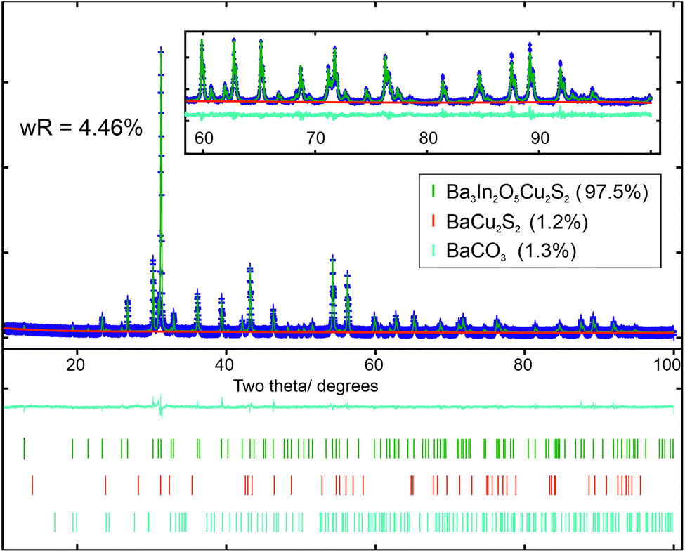 | ||
| Fig. 1 Rietveld refinement of I4/mmm structure of Ba3In2O5Cu2S2 to diffraction data, with lattice parameters a = 4.1862 Å and c = 27.444 Å. Upper section: diffraction data is in blue, model is in green and background in red. Inset shows the high angle region from 60° to 100° 2θ. Lower section shows the difference curve (cyan) and tick marks indicating the positions of the peaks of, in descending order: Ba3In2O5Cu2S2 (green), BaCu2S2 (red) and BaCO3 (cyan). | ||
| Ba3Sc2O5Cu2S2 | Ba3Sc1.5In0.5O5Cu2S | Ba3ScInO5Cu2S2 | Ba3Sc0.5In1.5O5Cu2S | Ba3In2O5Cu2S2 | |
|---|---|---|---|---|---|
| Lattice parameter a/Å | 4.1458(2) | 4.1577(2) | 4.1680(3) | 4.1772(2) | 4.1862(1) |
| 4.15 | 4.19 | ||||
| Lattice parameter c/Å | 27.136(2) | 27.218(2) | 27.317(4) | 27.401(2) | 27.444(1) |
| 27.38 | 27.73 | ||||
| Volume/Å3 | 466.42(6) | 470.50(5) | 474.55(8) | 478.12(6) | 480.95(2) |
| 471.48 | 487.91 | ||||
| Data points | 4444 | 4444 | 4444 | 4444 | 4345 |
| Reflections (main phase) | 100 | 101 | 101 | 102 | 98 |
| Parameters | 34 | 29 | 24 | 30 | 23 |
| Purity | 95.6% | 96.1% | 98.7% | 97.9% | 97.5% |
| wRp | 3.72% | 3.43% | 3.99% | 3.16% | 4.46% |
| RF2 | 3.32% | 2.18% | 3.48% | 2.28% | 3.12% |
| Chi2 | 2.04 | 1.98 | 2.38 | 1.96 | 1.93 |
| Ba3In2O5Cu2S2* | Ba3In2O5Cu2S1.5Se0.5 | Ba3In2O5Cu2SSe | Ba3In2O5CuS0.5Se1.5 | Ba3In2O5Cu2Se2 | |
|---|---|---|---|---|---|
| Lattice parameter a/Å | 4.1862(1) | 4.1958(2) | 4.2060(2) | 4.2138(2) | 4.2225(1) |
| 4.19 | 4.22 | ||||
| Lattice parameter c/Å | 27.444(1) | 27.576(2) | 27.716(2) | 27.841(2) | 27.985(1) |
| 27.73 | 28.03 | ||||
| Volume/Å3 | 480.95(2) | 485.47(5) | 490.31(5) | 494.35(6) | 498.95(4) |
| 487.91 | 499.67 | ||||
| Data points | 4345 | 4444 | 4444 | 4148 | 4444 |
| Reflections (main phase) | 98 | 106 | 108 | 98 | 111 |
| Parameters | 23 | 30 | 30 | 30 | 32 |
| Purity | 97.5% | 98.7% | 98.6% | 98.5% | 97.8% |
| wRp | 4.46% | 3.87% | 4.11% | 4.55% | 4.28% |
| RF2 | 3.12% | 3.55% | 3.85% | 4.74% | 3.30% |
| Chi2 | 1.93 | 1.72 | 1.93 | 3.50 | 2.19 |
The results of the analysis of the diffraction data were supported by energy dispersive X-ray spectroscopy (EDX). For each sample, EDX data were collected on 5 different particles chosen at random, and the elemental composition quantified based on the expected heavy elements, with oxygen excluded from the analysis due to presence of environmental contaminants containing oxygen preventing reliable estimation of the amount of this element in the sample. The average elemental composition for each sample resulting from this analysis is shown graphically in Fig. 2, alongside the values expected from the targeted stoichiometry as a guide. These show a good match between the experimental and expected values, so that we can conclude that both the XRD and EDX data confirm that the target phases have been made as intended. The end member Ba3Sc2O5Cu2S2 has been previously reported,19 however to the best of our knowledge the solid solution end members Ba3In2O5Cu2S2 and Ba3In2O5Cu2Se2, alongside all the intermediate phases, are reported in this work for the first time.
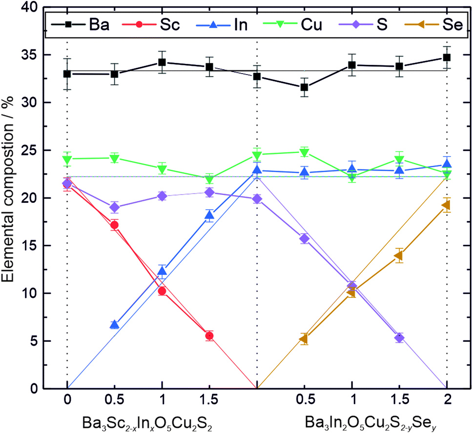 | ||
| Fig. 2 Plot of elemental composition as determined by EDX excluding oxygen, for the two solid solutions: Ba3Sc2−xInxO5Cu2S2 and Ba3In2O5Cu2S2−ySey. Thin solid lines represent the percentage of each element expected based on the target composition. | ||
Lattice parameters for the layered oxychalcogenides derived from the Rietveld refined structural models, as a function of composition, are displayed in Fig. 3. These show a good approximation to Vegard's law for both solid solutions. In series 1 the replacement of the smaller scandium ion (radius of 0.75 Å) with the larger indium ion (0.80 Å) leads to a steady increase in both the a and c lattice parameters, with an increase of approximately 1% in both a and c once full replacement by indium is achieved. In series 2, where sulphur (1.84 Å) is replaced with selenium (1.98 Å) in Ba3In2O5Cu2S2, we observe a similar increase in both a and c lattice parameters. Coincidently, the increase in a in series 2 occurs at a similar rate as a function of the fraction of substitution as in series 1, although that of the c parameter is greater. Overall in series 2 there is an increase of 0.9% in a in series 2 for the full substitution of selenium, but an expansion of approximately 2% in the c parameter.
 | ||
| Fig. 3 Plot of lattice parameters for the Ba3Sc2−xInxO5Cu2S2 and Ba3In2O5Cu2S2−ySey solid solutions (x, y = 0, 0.5, 1, 1.5 2) as a function of composition. The a lattice parameter scale is to the left and values are shown as black squares. The c lattice parameter scale is to the right, and values are shown with hollow triangles. Error bars are smaller than the symbols used, and the dashed lines are guides for the eye, and indicative of the Vegard law relationship between lattice dimensions and composition. | ||
The results of the refinement of the atomic site positions within the unit cell models provides bond lengths and angles, and therefore insight into the changes in the structures across the solid solutions that drive the overall expansion of the unit cells. The limitations of laboratory X-ray diffraction equipment mean that the position of the light oxygen atoms can only be ascertained with limited confidence. However, it is still possible to draw conclusions regarding the general trends, and with greater confidence for the heavier atoms. Fig. 4 shows variations in key bond lengths and angles across the structures as a function of composition. These values can be found tabulated in the ESI in Table S3.†
 | ||
| Fig. 4 Left: Schematic diagram of the unit cell of the Ba3MO5Cu2Ch2 structures, where M = Sc, In and Ch = S, Se. Centre and Right: Plots of the key angles (triangles) and bond lengths (squares) of the oxide and chalcogenide blocks respectively as a function of composition, including the variation in overall block height for each (circles). Where they are not shown, error bars are smaller than the symbols used. | ||
The general unit cell diagram for these samples is shown in Fig. 4, and highlights that the structure can be considered as layered blocks of [Ba3M2O5]2+ and [Cu2Ch2]2−, where M = Sc or In and Ch = S or Se. The nature of this layering means that any change in one of the blocks that expands it parallel to the [100] direction must be matched by an expansion in that direction in the other block in order to maintain a commensurate a lattice parameter. For example, an expansion of the oxide block in the [100] direction due to a substitution would inevitably force a change in the bonding or geometry to the chalcogenide layer even if it remains compositionally unchanged. In contrast changes to the dimensions of a block parallel to the [001] direction can occur independently, without necessarily affecting the structure of the other layer. Thus changes to the structure that lead to changes in the a lattice parameter are dependent upon both oxide and chalcogenide blocks, whereas changes in the c direction can occur due to either variations in the height of the oxide block, the chalcogenide layer, or the interlayer spacing, and these can be independent of each other.
In series 1 there is steady overall increase in the value of both the a and c lattice parameters of approximately 1% from Ba3Sc2O5Cu2S2 to Ba3In2O5Cu2S2. The key structural change is the substitution of the larger indium into the oxide block which drives the 1% expansion of the cell in the a direction. The geometry of the Sc/In site is pyramidal, and the equatorial metal oxygen bond increases in length by ∼0.7% across the series, accounting for the majority of the expansion in the a lattice parameter, the rest of the expansion coming from a small change in the geometry with a decrease in the Oax–M–Oeq (M = Sc/In) bond angle from 97.8(5)° to 96.7(4)° as the average metal site position moves towards the sulfur. The most significant bond length change is the increase in the axial M–O bond length from 1.98(1) Å to 2.062(3) Å, an increase of ∼4%. It is this increase which drives the overall expansion of the cell in the c direction. The response of the compositionally constant copper sulphide layer to the expansion in the a lattice parameter is a reduction in the block height parallel to the [001] direction, counter to the overall expansion of the c lattice parameter. As might be expected the Cu–S bond length remains approximately constant, with the change in the height of the copper containing layer instead being driven by a distortion in the copper geometry, observed by the increase in the S–Cu–S angle from 113.7(5)° to ∼115.8(4)°. Therefore, the decrease in the sulfide block height with expansion in the [001] direction is driven by changes in the oxide block, but the overall size of the unit cell increases in the c direction because of the larger increase in the height of the [Ba3M2O5]2+ layer.
This accordion-like scissoring of the copper sulfide block with an inverse relationship between the block height and the a lattice parameter due to distortions in the copper sulfur bond angles follows the trend observed in the oxysulfides, and accounts for the compatibly of the copper chalcogenide layers with a diversity of metal oxide layers of differing dimensions. Prior works on related materials have found examples of copper sulfide layers that can accommodate values of a lattice parameter as low as 3.83 Å in Ca4Fe2O6Cu2S2 and as high as 4.08 Å in Sr3Sc2O5Cu2S2,22,49 or up to 4.12 Å if the fluoride layered BaFCuS is considered.50 The values of a lattice parameter we have identified for the Ba3Sc2−xInxO5Cu2S2 solid solution of 4.146 Å to 4.186 Å significantly extends the range of feasible dimensions for layered copper sulfides, and to our knowledge are the largest values yet reported. The end member Ba3In2O5Cu2S2 may well be reaching the limit of what is possible for a stable [Cu2S2]2− layer, with a S–Cu–S angle of approximately 116° showing significantly higher distortion away from tetrahedral geometry than any prior example.
In series 2, Ba3In2O5Cu2S2−ySey, the expansion of the lattice parameters is driven by changes in the chalcogenide layer, in contrast to series 1 where it occurs in the oxide layer. With the substitution of the larger selenium for sulphur we see the expected increase in the copper chalcogenide bond length, of 2.7% across the series. Simultaneously we observe a relaxation of the copper environment back towards a more ideal tetrahedral geometry, with the Ch–Cu–Ch bond angle decreasing to 112.5(1)° indicating that the larger copper selenide layer is a better, less strained match for the [Ba3In2O5]2+ layer than the copper sulfide layer. The combined effect of these changes is an expansion of the a lattice parameter of ∼0.9%, and also a very significant increase in the height of the chalcogenide block in the [001] direction across the series of 7%. The response of the now compositionally unchanging [Ba3In2O5]2+ layer to the increase in the a lattice parameter is a compensatory decrease in height parallel to the [001] direction, although the effect is smaller than the similar compensation effect observed in the chalcogenide layer in series 1. The equatorial In–O bond length increases slightly, by 0.5% across the series, while the apical In–O length remains approximately constant. The key effect of the changing dimensions of the oxide block is a change in the geometry of the indium ion with the O–In–O bond angle decreasing in order to accommodate the increase in the [100] direction, and this is the cause of the overall decrease in the height of the oxide block.
The results of the computational modelling of the structures of the end member compositions using the HSE06 functional and PBEsol functional are provided the ESI in Tables S4 and S5,† including the lattice parameters, bond lengths and bond angles. Each of the end member compounds displayed the same I4/mmm symmetry after geometric relaxation to within 0.01 Å−1. Each of the calculated lattice parameters are within 2% of the experimental values owing to the efficacy of both HSE06 and PBEsol in describing the structural properties of this family of layered oxychalcogenide.19,27 As finite temperatures are typically neglected from DFT, these results indicate that there is minimal thermal expansion and change to the structural properties between 0 K and RTP and thus it is unlikely that the calculated electronic properties will deviate from those observed through experiment. As expected, the substitution of S for Se increases the a and c parameters and increases all of the bond lengths respectively whilst the Cu–Ch–Cu (Ch = S, Se) bond angle decreases. This results in a contraction of the [Cu2Ch2]2− layers shown by the Ba–Ba interlayer distances, or ‘block height’ also seen in the experimental values. In terms of bond lengths, the layers typically remain independent, i.e. between Ba3Sc2O5Cu2S2 and Ba3In2O5Cu2S2 the Cu–Ch and Cu–Cu distances show minimal changes, yet within the [Ba3M2O5]2+ layer, the Ba–O and M–O distances undergo a larger change than between Ba3In2O5Cu2S2 and Ba3In2O5Cu2Se2. As mentioned in previous work, the influence of structure as well as composition plays a distinct role in the tunability of these layered oxychalcogenide semiconductors.19
In order to estimate the band gaps for the materials, diffuse reflection spectra were recorded on each of the powder samples and the reflectance data were modelled using the Kubelka–Munk function, f(R). Tauc plots of [f(R)hυ]2 against photon energy (hυ) were used to estimate the direct band gap by extrapolation of a tangent from the point of inflection to the abscissa, and can be found in ESI Fig. S4.† This analysis gave band gap values of 3.27(5) eV for Ba3Sc2O5Cu2S2, 1.77(5) eV for Ba3In3O5Cu2S2, and 1.32(5) eV for Ba3In3O5Cu2Se2, the end members of the solid solutions. For the intermediate compositions, there is an approximately linear relationship between the composition and the experimentally determined band gap, as shown in Fig. 5(a), although with a slight deviation for the series 1 solution, Ba3Sc2−xInxO5Cu2S2.
 | ||
| Fig. 5 (a): Experimentally determined band gap values as a function of composition for the solid solutions Ba3Sc2−xInxO5Cu2S2 and Ba3In2O5Cu2S2−ySey. Dotted lines represent linear relationship between end members, and are shown as a guide for the eye. (b–d): Band structures for Ba3Sc2O5Cu2S2, and Ba3Sc2O5Cu2S2, and Ba3Sc2O5Cu2S2 respectively. In each panel the valence and conduction bands are coloured blue and orange respectively and the valance band maximum is set to 0 eV. (e–g): Calculated density of states diagrams for the three end member compounds. In each panel the valence band maximum (VBM) is set to 0 eV. For the two In-containing compounds, (f) and (g), a scaled view of the CBM is inset. | ||
The band structures of the three end members were computationally modelled, to help understand the changes in band gap, and can be seen in Fig. 5(b)–(d), with the density of states diagrams in Fig. 5(e)–(g). For each compound the valence band maxima (VBM) is composed approximately of 50![[thin space (1/6-em)]](https://www.rsc.org/images/entities/char_2009.gif) :50 Cu 3d:Ch p states meaning that the [Cu2Ch2]2− layer dominates the p-type conductivity in these systems and has been noted previously.19,27 The full break down of states at the VBM and conduction band minimum (CBM) are given in the ESI in Table S6.† The majority of the O 2p states lie around −6 eV to −2 eV for each compound, owing to the electronegativity of oxygen and the reason why typically in metal oxide photocatalysts such as TiO2 the VBM lies deep compared to the redox potentials of water.51 It is expected that a better bulk band alignment will exist for each of these compounds due to the VBM moving towards the vacuum due to the overlap between Cu 3d and Ch p. This has the added effect of increasing dispersion at the VBM giving rise to lower effective masses. For Ba3Sc2O5Cu2S2, Ba3In2O5Cu2S2 and Ba3In2O5Cu2Se2, the direct fundamental band gaps are modelled as 3.04 eV, 1.37 eV and 1.09 eV respectively and are direct (at Γ) with the exception of Ba3Sc2O5Cu2S2 where the VBM occurs at Γ and the CBM at the X point. The energy difference between the indirect and direct band gap (at Γ) is <2 meV, however it is well known that this type of behaviour gives rise to enhanced exciton lifetimes such as seen in anatase TiO2 or BiOX (X = Cl, Br, I) photocatalysts.52,53 In all three end member compounds there exists two degenerate bands at the VBM resulting in heavy and light hole effective masses. The full results of the effective mass modelling are given in the ESI in Table S7,† however herein the light effective masses will be documented, as the path of least resistance will likely be taken. The hole effective masses in the [Cu2Ch2]2− plane can be found at Γ–N and Γ–Z whilst the direction corresponding to the interplanar direction is given by Γ–X. The Γ–X direction results in highly flat bands as expected with (light) hole effective masses of ∼42 me, ∼84 me and ∼41 me respectively. For Ba3Sc2O5Cu2S2, Ba3In2O5Cu2S2 and Ba3In2O5Cu2Se2 the light effective masses in the Γ–N and Γ–Z direction are 0.44 me and 0.65 me, 0.38 me and 0.51 me, and 0.26 me and 0.36 me respectively. It is clear then, that both the increase in a lattice parameter as well as the exchange of sulfur for selenium results in a lowering of the valence band effective mass.
:50 Cu 3d:Ch p states meaning that the [Cu2Ch2]2− layer dominates the p-type conductivity in these systems and has been noted previously.19,27 The full break down of states at the VBM and conduction band minimum (CBM) are given in the ESI in Table S6.† The majority of the O 2p states lie around −6 eV to −2 eV for each compound, owing to the electronegativity of oxygen and the reason why typically in metal oxide photocatalysts such as TiO2 the VBM lies deep compared to the redox potentials of water.51 It is expected that a better bulk band alignment will exist for each of these compounds due to the VBM moving towards the vacuum due to the overlap between Cu 3d and Ch p. This has the added effect of increasing dispersion at the VBM giving rise to lower effective masses. For Ba3Sc2O5Cu2S2, Ba3In2O5Cu2S2 and Ba3In2O5Cu2Se2, the direct fundamental band gaps are modelled as 3.04 eV, 1.37 eV and 1.09 eV respectively and are direct (at Γ) with the exception of Ba3Sc2O5Cu2S2 where the VBM occurs at Γ and the CBM at the X point. The energy difference between the indirect and direct band gap (at Γ) is <2 meV, however it is well known that this type of behaviour gives rise to enhanced exciton lifetimes such as seen in anatase TiO2 or BiOX (X = Cl, Br, I) photocatalysts.52,53 In all three end member compounds there exists two degenerate bands at the VBM resulting in heavy and light hole effective masses. The full results of the effective mass modelling are given in the ESI in Table S7,† however herein the light effective masses will be documented, as the path of least resistance will likely be taken. The hole effective masses in the [Cu2Ch2]2− plane can be found at Γ–N and Γ–Z whilst the direction corresponding to the interplanar direction is given by Γ–X. The Γ–X direction results in highly flat bands as expected with (light) hole effective masses of ∼42 me, ∼84 me and ∼41 me respectively. For Ba3Sc2O5Cu2S2, Ba3In2O5Cu2S2 and Ba3In2O5Cu2Se2 the light effective masses in the Γ–N and Γ–Z direction are 0.44 me and 0.65 me, 0.38 me and 0.51 me, and 0.26 me and 0.36 me respectively. It is clear then, that both the increase in a lattice parameter as well as the exchange of sulfur for selenium results in a lowering of the valence band effective mass.
The composition of the CBM is largely determined by the [Ba3M2O5]2+ layer. In the case of Ba3In2O5Cu2S2 and Ba3In2O5Cu2S2, the CBM is dominated by In 5s states mixed with O 2s states with negligible contributions from Cu 4s, Ch ns states and Ba 6s states. This is in contrast with Ba3Sc2O5Cu2S2 where scandium states do not play a role and instead the CBM is made up of Ba 5d states mixed with Cu 3s + d and negligible O 2s + p states. The reasoning for this is due to the lower lying In s states compared to the Ba d states which results in lower band gaps despite the larger a lattice parameter from Ba3Sc2O5Cu2S2 to Ba3In2O5Cu2S2. The CBM dispersion difference between Ba3Sc2O5Cu2S2 and the In-containing compounds is distinctly noticeable in the band structures in Fig. 5, whereby the In 5s states form highly dispersive bands with effective masses of 0.95 me, 0.21 me and 0.19 me respectively. Parallels can be made with the flagship n-type conducting transparent conducting oxide: In2O3 which also show the same low CBM effective masses of ∼0.22 me.54 In practice this means that Ba3In2O5Cu2S2 and Ba3In2O5Cu2Se2 will possess high electron mobility which will aid transport of photoexcited electrons to the surface of the material to perform catalysis.55 The In-based systems may also be bipolar semiconductors, a property which has been shown to exist in delafossite CuInO2.56,57
The modelled band structures provide insight into the observed experimental trends in the band gap. In series 1 the change in the composition of the CBM moves it lower in energy towards the valance band with increasing indium content, while the VBM itself remains undisturbed. The other key effect of the exchange of indium for scandium in the first series, as observed in analysis of the X-ray diffraction data, is in the expansion of the lattice parameters and an increase in the Cu–Cu distance. This has been previously shown to lead to a small increase in band gap due to decreased dispersion of the valence and conduction bands under the influence of the Cu–Cu interactions.12 The effect is expected to be approximately only +0.04 eV for the increase in Cu–Cu distance in the Ba3Sc2−xInxO5Cu2S2 solution, however it may account for the small deviation from trend observed for the latter members of the solution, as shown in the first half of Fig. 5(a). In the second solid solution the exchange of sulphur in Ba3In2O5Cu2S2 leads to a shift in the valance band maximum towards the vacuum and giving an overall decrease in the band gap. The effect across the whole of the solution is a decrease of the band gap by 0.45 eV. This is comparable to similar observed differences in band gap energy for pairs of layered oxychalcogenides where both the oxysulfide and oxyselenide are known, for example, Sr3Sc2O5Cu2Ch2 with band gaps of 3.10 eV for Ch = S and 2.90 eV when Ch = Se,6,58 and LaOCuCh with band gaps 3.14 eV (Ch = S) and 2.82 eV (Ch = Se).59
The optical absorption coefficients were also simulated and can be found in the ESI in Fig. S5,† as a function of photon energy. The optical band gaps for Ba3Sc2O5Cu2S2, Ba3In2O5Cu2S2 and Ba3In2O5Cu2Se2, are calculated to be 3.24 eV, 1.84 eV and 1.48 eV respectively. This corresponds well with those gained in experiment (3.27 eV, 1.77 eV and 1.32 eV respectively). A strong (steep) absorption corresponds to an increased likelihood of photoexcited charge carriers and therefore a greater potential for photocatalytic activity. Each end member compound has a relatively steep absorption, particularly Ba3Sc2O5Cu2S2, however for the series 2 compounds the onset is more gradual. For Ba3In2O5Cu2S2 and Ba3In2O5Cu2Se2 the difference in optical band gaps is not as large as compared to Ba3In2O5Cu2S2 and Ba3Sc2O5Cu2S2. Thus solid solutions of Ba3In2O5Cu2S2−ySey will not largely affect the optical properties but will affect the electronic properties by raising the VBM and increasing VBM curvature for more mobile holes evident from the band structures and effective masses.
Photocatalytic testing was carried out using degradation of the blue dye DCIP in the presence of glycerol as a sacrificial oxidant, using an unfiltered solar simulator as the light source. 5 mg samples of oxychalcogenide powders were loaded with cobalt oxide oxidation co-catalyst, at approximately 0.4 wt% in order to enhance the observable rates.60,61 The powder samples were continuously stirred to ensure homogeneous dispersion in the test solution across the 3 hour test time, after which the solution was separated from the powder using a centrifuge and the change in dye concentration determined. A control experiment where the dye solution was exposed to the solar simulator for 3 hours without any powder sample present found that no degradation occurs within the error of the measurement. The majority of the co-catalyst loaded oxychalcogenide samples were found to be active photocatalysts, except for Ba3In2O5Cu2S0.5Se1.5. This data can be seen in Table 3. The most active samples were the two with the largest band gaps, Ba3Sc2O5Cu2S2 and Ba3Sc1.5In0.5Cu2S2 where 27% and 23% of the dye was found to have degraded, respectively. The percentages of the dye degraded for all the samples are shown in Fig. 6, where the remaining active samples have degradation fractions over 3 hours of between 5% and 15%. Across both solid solutions there is an inverse correlation between the extent of photocatalytic dye degradation and the band gap size. DCIP dye degradation is an indicative test, and the greater rates observed for the materials with the larger band gaps is likely to be due to the increased over potential for the photocatalytic reaction. However, the results of dye degradation tests need to be considered with caution, as although they can indicate photocatalytic activity, they cannot be used as a guarantee that the catalyst will be active for the more challenging water splitting reaction. Dye degradation can also depend on the surface area, the spectral absorption overlap with the dye, and the photocatalyst surface charge.62 For our solid solutions the samples are sufficiently similar that these factors should not prevent a relative comparison of photocatalytic activity, but further research will be necessary to confirm if they are capable of total organic carbon removal, or water splitting.
| Ba3Sc2−xInxO5Cu2S2 | Ba3In2O5Cu2S2−ySey | |||||||||
|---|---|---|---|---|---|---|---|---|---|---|
| x/y | 0 | 0.5 | 1 | 1.5 | 2 | 0 | 0.5 | 1 | 1.5 | 2 |
| Band gap/eV | 3.27(5) | 2.80(5) | 2.41(5) | 2.09(5) | 1.77(5) | 1.77(5) | 1.65(5) | 1.55(5) | 1.44(5) | 1.32(5) |
| DCIP degradation | 27.0% | 22.9% | 14.8% | 15.4% | 14.5% | 14.5% | 5.9% | 3.8% | 0.3% | 5.5% |
 | ||
| Fig. 6 Plot of fraction of DCIP dye degraded after 3 hours exposure to a solar simulator in the presence of a sample of each of the oxychalcogenide powders, and a control with no sample present. | ||
Conclusions
We have demonstrated the synthesis of two new solid solutions, Ba3Sc2−xInxO5Cu2S2 and Ba3In2O5Cu2S2−ySey, and shown that almost all of these display photocatalytic activity. The shared end member Ba3In2O5Cu2S2 has a basal lattice parameter of 4.1861 Å, which is the largest yet reported for a layered oxysulfide containing anti-litharge structured copper sulphide layer. This therefore expands the upper range for the use of the [Cu2S2]2− structural unit when considering a building block approach to materials design.Spectroscopic analysis has shown that the with the two solid solutions it is possible to select, through appropriate choice of composition, a photocatalytic material with any band gap ranging from 3.30 eV to 1.32 eV. This spans the visible spectrum from the near UV to the near IR, although the driving force behind the change in band gap differs for the two solid solutions. From Ba3Sc2O5Cu2S2 to Ba3In2O5Cu2S2 the conduction band minimum decreases, while from Ba3In2O5Cu2S2 to Ba3In2O5Cu2S2 the valence band maximum increases. The ability to tune the band gap and band edge positions through composition in the two solid solutions is a key feature that could be used in the future in the optimisation of the absorber in a water splitting photocatalyst system.
Data availability
All data supporting this study are openly available from the University of Southampton repository at DOI: 10.5258/SOTON/D1457.Conflicts of interest
There are no conflicts of interest.Acknowledgements
GH would like to acknowledge the financial support of the EPSRC through the grant EP/T011793/1. BADW and DOS would like to acknowledge support from the European Research Council, ERC, (Grant 758345). This work made use of the ARCHER UK National Supercomputing Service (http://www.archer.ac.uk) via our membership of the UK's HEC Materials Chemistry Consortium, which is also funded by the EPSRC (EP/L000202). The UCL Legion and Grace HPC Facilities (Legion@UCL and Grace@UCL) were also used in the completion of this work. Finally BADW would like to acknowledge support from the Research Council of Norway (Project no. 275810).References
- D. Johrendt and R. Pottgen, Angew. Chem., Int. Ed., 2008, 47, 4782–4784 CrossRef CAS.
- X. Zhu, F. Han, G. Mu, P. Cheng, B. Shen, B. Zeng and H.-H. Wen, Phys. Rev. B: Condens. Matter Mater. Phys., 2009, 79, 220512 CrossRef.
- H. Ogino, Y. Matsumura, Y. Katsura, K. Ushiyama, S. Horii, K. Kishio and J.-i. Shimoyama, Supercond. Sci. Technol., 2009, 22, 075008 CrossRef.
- X. Zhu, F. Han, G. Mu, B. Zeng, P. Cheng, B. Shen and H.-H. Wen, Phys. Rev. B: Condens. Matter Mater. Phys., 2009, 79, 024516 CrossRef.
- H. Hiramatsu, K. Ueda, H. Ohta, M. Hirano, M. Kikuchi, H. Yanagi, T. Kamiya and H. Hosono, Appl. Phys. Lett., 2007, 91, 012104 CrossRef.
- M.-L. Liu, L.-B. Wu, F.-Q. Huang, L.-D. Chen and I.-W. Chen, J. Appl. Phys., 2007, 102, 116108 CrossRef.
- S. Jin, X. Chen, J. Guo, M. Lei, J. Lin, J. Xi, W. Wang and W. Wang, Inorg. Chem., 2012, 51, 10185–10192 CrossRef CAS.
- Q. Wang, M. Nakabayashi, T. Hisatomi, S. Sun, S. Akiyama, Z. Wang, Z. Pan, X. Xiao, T. Watanabe, T. Yamada, N. Shibata, T. Takata and K. Domen, Nat. Mater., 2019, 18, 827–832 CrossRef CAS.
- M. Yashima, K. Ogisu and K. Domen, Acta Crystallogr., Sect. B: Struct. Sci., 2008, 64, 291–298 CrossRef CAS.
- A. Ishikawa, T. Takata, T. Matsumura, J. N. Kondo, M. Hara, H. Kobayashi and K. Domen, J. Phys. Chem. B, 2004, 108, 2637–2642 CrossRef CAS.
- A. Ishikawa, T. Takata, J. N. Kondo, M. Hara, H. Kobayashi and K. Domen, J. Am. Chem. Soc., 2002, 124, 13547–13553 CrossRef CAS.
- S. J. Clarke, P. Adamson, S. J. C. Herkelrath, O. J. Rutt, D. R. Parker, M. J. Pitcher and C. F. Smura, Inorg. Chem., 2008, 47, 8473–8486 CrossRef CAS.
- A. Ishikawa, Y. Yamada, T. Takata, J. N. Kondo, M. Hara, H. Kobayashi and K. Domen, Chem. Mater., 2003, 15, 4442–4446 CrossRef CAS.
- F. E. Osterloh, Chem. Mater., 2008, 20, 35–54 CrossRef CAS.
- K. Maeda and K. Domen, J. Phys. Chem. C, 2007, 111, 7851–7861 CrossRef CAS.
- A. B. Ellis, S. W. Kaiser, J. M. Bolts and M. S. Wrighton, J. Am. Chem. Soc., 1977, 99, 2839–2848 CrossRef CAS.
- J. R. Bolton, S. J. Strickler and J. S. Connolly, Nature, 1985, 316, 495–500 CrossRef CAS.
- Y. Inoue, Energy Environ. Sci., 2009, 2, 364–386 RSC.
- B. A. D. Williamson, G. J. Limburn, G. W. Watson, G. Hyett and D. O. Scanlon, Matter, 2020, 3, 759–781 CrossRef.
- O. Y. Mruz, V. K. Pecharsky, A. N. Sobolev and O. I. Bodak, Kristallografiya, 1990, 35, 202–204 CAS.
- W. J. Zhu and P. H. Hor, J. Solid State Chem., 1997, 134, 128–131 CrossRef CAS.
- K. Otzschi, H. Ogino, J. Shimoyama and K. Kishio, J. Low Temp. Phys., 1999, 117, 729–733 CrossRef CAS.
- H. Ogino, Y. Katagi, J.-i. Shimoyama, K. Yamanoi, M. Tsuboi, T. Shimizu, N. Sarukura and K. Kishio, Opt. Mater., 2014, 36, 1978–1981 CrossRef CAS.
- F. Hummel, M. Tegel, B. Gerke, R. Pöttgen and D. Johrendt, Zeitschrift für Naturforschung B, 2015, 70, 671–676 CAS.
- G. F. Chen, T. L. Xia, H. X. Yang, J. Q. Li, P. Zheng, J. L. Luo and N. L. Wang, Supercond. Sci. Technol., 2009, 22, 072001 CrossRef.
- D. Johrendt, H. Hosono, R. D. Hoffmann and R. Pottgen, Z. Kristallogr.–Cryst. Mater., 2011, 226, 435–446 CAS.
- D. O. Scanlon and G. W. Watson, Chem. Mater., 2009, 21, 5435–5442 CrossRef CAS.
- G. Hyett, Z. A. Gal, C. F. Smura and S. J. Clarke, Chem. Mater., 2008, 20, 559–566 CrossRef CAS.
- B. H. Toby and R. B. Von Dreele, J. Appl. Crystallogr., 2013, 46, 544–549 CrossRef CAS.
- P. Kubelka, J. Opt. Soc. Am., 1948, 38, 448–457 CrossRef CAS.
- J. Tauc, Mater. Res. Bull., 1968, 3, 37–46 CrossRef CAS.
- A. E. Maegli, S. Pokrant, T. Hisatomi, M. Trottmann, K. Domen and A. Weidenkaff, J. Phys. Chem. C, 2014, 118, 16344–16351 CrossRef CAS.
- A. Mills and M. McGrady, J. Photochem. Photobiol., A, 2008, 193, 228–236 CrossRef CAS.
- G. Kresse and J. Furthmuller, Comput. Mater. Sci., 1996, 6, 15–50 CrossRef CAS.
- G. Kresse and J. Furthmuller, Phys. Rev. B: Condens. Matter Mater. Phys., 1996, 54, 11169–11186 CrossRef CAS.
- G. Kresse and J. Hafner, Phys. Rev. B: Condens. Matter Mater. Phys., 1993, 47, 558–561 CrossRef CAS.
- G. Kresse and J. Hafner, Phys. Rev. B: Condens. Matter Mater. Phys., 1994, 49, 14251–14269 CrossRef CAS.
- A. V. Krukau, O. A. Vydrov, A. F. Izmaylov and G. E. Scuseria, J. Chem. Phys., 2006, 125(22), 223106 CrossRef.
- P. E. Blochl, Phys. Rev. B: Condens. Matter Mater. Phys., 1994, 50, 17953–17979 CrossRef.
- A. M. Ganose, A. J. Jackson and D. O. Scanlon, Journal of Open Source Software, 2018, 3, 717–719 CrossRef.
- B. Adolph, J. Furthmüller and F. Bechstedt, Phys. Rev. B: Condens. Matter Mater. Phys., 2001, 63, 125108 CrossRef.
- M. Gajdos, K. Hummer, G. Kresse, J. Furthmuller and F. Bechstedt, Phys. Rev. B: Condens. Matter Mater. Phys., 2006, 73, 045112 CrossRef.
- A. Togo and I. Tanaka, Scr. Mater., 2015, 108, 1–5 CrossRef CAS.
- G. I. Csonka, J. P. Perdew, A. Ruzsinszky, P. H. T. Philipsen, S. Lebegue, J. Paier, O. A. Vydrov and J. G. Angyan, Phys. Rev. B: Condens. Matter Mater. Phys., 2009, 79, 155107 CrossRef.
- J. P. Perdew, A. Ruzsinszky, G. I. Csonka, O. A. Vydrov, G. E. Scuseria, L. A. Constantin, X. L. Zhou and K. Burke, Phys. Rev. Lett., 2008, 100, 136406 CrossRef.
- J. P. Devilliers, Am. Mineral., 1971, 56, 758–767 CAS.
- J. E. Iglesias, K. E. Pachali and H. Steinfink, J. Solid State Chem., 1974, 9, 6–14 CrossRef CAS.
- W. O. Milligan, L. W. Vernon, H. A. Levy and S. W. Peterson, J. Phys. Chem., 1953, 57, 535–537 CrossRef CAS.
- D. O. Charkin, A. V. Sadakov, O. E. Omel’yanovskii and S. M. Kazakov, Mater. Res. Bull., 2010, 45, 2012–2016 CrossRef CAS.
- H. Yanagi, S. Park, A. D. Draeseke, D. A. Keszler and J. Tate, J. Solid State Chem., 2003, 175, 34–38 CrossRef CAS.
- B. A. D. Williamson, J. Buckeridge, N. P. Chadwick, S. Sathasivam, C. J. Carmalt, I. P. Parkin and D. O. Scanlon, Chem. Mater., 2019, 31, 2577–2589 CrossRef CAS.
- A. M. Ganose, M. Cuff, K. T. Butler, A. Walsh and D. O. Scanlon, Chem. Mater., 2016, 28, 1980–1984 CrossRef CAS.
- A. M. Alotaibi, B. A. D. Williamson, S. Sathasivam, A. Kafizas, M. Alqahtani, C. Sotelo-Vazquez, J. Buckeridge, J. Wu, S. P. Nair, D. O. Scanlon and I. P. Parkin, ACS Appl. Mater. Interfaces, 2020, 12, 15348–15361 CrossRef CAS.
- J. E. N. Swallow, B. A. D. Williamson, S. Sathasivam, M. Birkett, T. J. Featherstone, P. A. E. Murgatroyd, H. J. Edwards, Z. W. Lebens-Higgins, D. A. Duncan, M. Farnworth, P. Warren, N. H. Peng, T. L. Lee, L. F. J. Piper, A. Regoutz, C. J. Carmalt, I. P. Parkin, V. R. Dhanak, D. O. Scanlon and T. D. Veal, Mater. Horiz., 2020, 7, 236–243 RSC.
- X. Zhou and H. Dong, ChemCatChem, 2019, 11, 3686–3713 Search PubMed.
- K. G. Godinho, B. J. Morgan, J. P. Allen, D. O. Scanlon and G. W. Watson, J. Phys.: Condens. Matter, 2011, 23, 334201 CrossRef CAS.
- M. Sasaki and M. Shimode, J. Phys. Chem. Solids, 2003, 64, 1675–1679 CrossRef CAS.
- Y. Iwasa, H. Ogino, D. Song, K. Yamanoi, T. Shimizu, J. Ueda, S. Tanabe and N. Sarukura, Opt. Mater., 2018, 84, 205–208 CrossRef CAS.
- K. Ueda and H. Hosono, J. Appl. Phys., 2002, 91, 4768–4770 CrossRef CAS.
- F. Oehler and S. G. Ebbinghaus, Solid State Sci., 2016, 54, 43–48 CrossRef CAS.
- F. Oehler, R. Naumann, R. Köferstein, D. Hesse and S. G. Ebbinghaus, Mater. Res. Bull., 2016, 73, 276–283 CrossRef CAS.
- S. Bae, S. Kim, S. Lee and W. Choi, Catal. Today, 2014, 224, 21–28 CrossRef CAS.
Footnote |
| † Electronic supplementary information (ESI) available: Fig. S1, S2 and S3: Rietveld refinements of X-ray diffraction patterns. Fig. S4: Tauc plots derived from experimental spectra, Fig. S5: calculated optical absorption data and Fig. S6: calculated phonon dispersion data. The ESI also includes tables S1 and S2: details of the refined structural model and table S3: the refined bond lengths and angles. Tables S4 and S5: structural details of the computational derived models, Table S6: data on the calculated VBM and CBM composition, and table S7: the calculated effective electron and hole masses. Fig. S7 Model and recorded IR spectra, S8 Position of Principle IR peaks. Table S8: tabulated IR data. See DOI: 10.1039/d0ta06629j |
| This journal is © The Royal Society of Chemistry 2020 |