 Open Access Article
Mechanisms of the cyclic (de)lithiation of RuO2†
Lin
Xu
 and
Carl V.
Thompson
 *
*
Department of Materials Science and Engineering, Massachusetts Institute of Technology, Cambridge, Massachusetts 02139, USA. E-mail: cthomp@mit.edu
First published on 10th October 2020
Abstract
RuO2 films can serve as high-performance electrodes for thin film lithium-ion batteries due to their large volumetric charge capacity, low rate sensitivity and excellent cyclability. Unlike other electrode materials, RuO2 films also do not require high temperature processing, making them suitable for integration with low-power CMOS circuits and for fabrication on flexible membranes. To determine the mechanisms through which Li is reversibly stored in RuO2 films, detailed characterization studies of sputtered thin films were carried out; galvanostatic and potentiostatic intermittent titration and cyclic voltammetry studies were coupled with ex situ selected area electron diffraction, X-ray photoelectron and Raman spectroscopy, optical and scanning electron microscopy, energy-dispersive X-ray spectroscopy and in situ electrochemical impedance spectroscopy. During lithiation, amorphous RuO2 is transformed to amorphous LixRuO2 through an alloying reaction and this is followed by a reversible side reaction to form an SEI layer. LixRuO2 then undergoes a conversion reaction to form a mixture of nanosized Ru and Li2O crystals, and finally at low voltages Li is inserted into the Ru/Li2O mixture. These reactions occur in a different sequence during delithiation and a large overpotential is required to reverse the conversion reaction, leading to a large energy loss during cycling. It is argued that this hysteretic behavior is associated with slow diffusive processes required for the conversion reactions. The methodology developed in this study can also be applied to other candidate thin film electrode materials and learnings from studies of thin films can be applied to more complex powder-based electrodes used in bulk batteries.
1. Introduction
While the use of lithium ion batteries (LIBs) is already pervasive, the range of applications for LIBs continues to rapidly grow, especially in association with the development of new Internet of Things (IoT) technologies.1 The broad extent and diversity of applications of LIBs drive studies for continuous improvements in the performance of known electrode materials and development of new materials. Electrode materials that store lithium through phase transitions and conversion reactions are attractive candidates for LIB electrodes due to their large capacities compared to intercalation materials.2–11 For metal oxides, a conversion reaction plays a particularly important role in providing high storage capacity. This reaction has the form:| MaXb + (bn)Li ↔ aM + bLinX. |
Recently, Perego et al.12 demonstrated that one conversion-reaction-based material, RuO2, had excellent performance as a potential cathode material for thin film LIBs for microsystems, for which full-cell voltages as low as 1 V are usable. RF-sputtered RuO2 thin films showed five times greater volumetric energy than RF-sputtered LiCoO2 thin films. Moreover, unlike other electrode materials, RuO2 films do not require high temperature processing, making them suitable for integration with low-power CMOS circuits and for fabrication on flexible membranes. The mechanical behavior during the lithiation/delithiation cycling of RuO2 thin films has been studied by Zhu et al.13,14 However, lithiation and delithiation mechanisms for multiply-cycled RuO2 are poorly understood due to the poor cyclability of powder-based electrodes,15 and an improved understanding is required for optimization of battery performance and yield of thin film electrodes.
The lithiation of RuO2 was first studied by Ohzuku et al.,16 and the mechanisms for Li storage have subsequently been studied in various ways, especially during the first discharge of single crystal particles. David et al. studied the shallow lithiation of RuO2, before the occurrence of conversion reaction.17 Balaya et al.15,18 used X-ray diffraction (XRD), Raman spectroscopy, high resolution transmission electron microscopy (HRTEM) and selected area electron diffraction (SAED) to show that crystalline RuO2 could form crystalline Ru and Li2O during the first lithiation and returned to nanocrystalline or amorphous RuO2 after the first delithiation. Gregorczyk et al.19 used in situ TEM and found that an intermediate phase LixRuO2 formed before the formation of Ru during the first lithiation. They also reported that during further cycles of a nanowire, the reaction between amorphous RuO2 and Ru/Li2O was only partially reversible. The existence of the intermediate phase LixRuO2 was also confirmed by Mao et al.20 using in situ TEM. Hassan et al.21 used first-principles calculations to investigate the first lithiation of RuO2 and argued that additional Li could reside at interfaces between Ru and Li2O. Hu et al.22 used XRD, XAS (X-ray absorption spectroscopy) and NMR (nuclear magnetic resonance) to demonstrate that the formation of Li2O and LiH from LiOH on the surface was responsible for the additional capacity of RuO2 during the late stage of the first lithiation, while based on TEM, XPS and GITT (Galvanostatic Intermittent Titration Techniques) experiments, Kim et al.23 argued that Li storage at interfaces between newly formed nanosized Ru metal and Li2O phases was responsible for the additional capacity. Emilie et al. reached the same conclusion using 6Li magic-angle spinning nuclear magnetic resonance.24
So far, most studies of the mechanisms of lithiation and delithiation of RuO2 have focused only on the first lithiation process starting from crystalline RuO2 powders in composite electrodes with binders. This might be partially due to the poor cyclability of these electrodes.15 However, an in situ TEM study19 using RuO2 nanowires has shown that after the first delithiation cycle, the RuO2 was in an amorphous form rather than a crystalline form. This indicates that the previous conclusions reached from studies of the first cycle do not necessarily apply during further cycles. Electrochemical data such as cyclic voltammetry (CV) curves were not provided for cycles after the first cycle. In addition, conversion-type LIB electrodes are often found to have a large voltage hysteresis, meaning that the voltage of charging (delithiation) is significantly higher than the voltage of discharging (lithiation).9,10,25–29 The voltage hysteresis for conversion-type LIB electrodes is generally larger than for intercalation30 and alloying31 electrodes. We found that RuO2 also has a large voltage hysteresis (Fig. S1†).
As a good candidate for thin-film electrode materials as well as an example of a conversion-reaction-based electrode material with complex reaction mechanisms, it is important that a more complete understanding of the mechanisms and kinetics of reversible storage of Li in RuO2 be developed, not only in the first cycles, but also during subsequent cycles. In many ways, thin films also provide an ideal form for mechanistic studies. Therefore, while studies of thin film electrodes serve to guide optimization for use in thin film batteries, they also provide a guide for development of conversion-reaction powder electrodes with improved cyclability and reduced hysteretic effects.
In this work, we performed detailed electrochemical and physical characterization of multiply-cycled sputtered thin film RuO2 samples. Individual reactions occurring in different voltage regimes were identified through a set of GITT and CV measurements designed for this purpose. Samples were then characterized in different states of charge using ex situ Selected Area Electron Diffraction (SAED), X-ray Photoelectron Spectroscopy (XPS), Raman spectroscopy, Optical Microscopy (OM), Scanning Electron Microscopy (SEM), Energy-dispersive X-ray Spectroscopy (EDS) and in situ Electrochemical Impedance Spectroscopy (EIS). The Potentiostatic Intermittent Titration Technique (PITT) and CV measurements on RuO2 thin films with different thicknesses were also performed to determine the rate limiting kinetic process that leads to the voltage hysteresis.
2. Experimental
Double-side polished aluminum oxide (99.6%, Al2O3, 250 μm thick, Stellar Ceramics) was used as the substrate for RuO2 thin film deposition. The aluminum oxide was cleaved into 5 mm by 8 mm pieces and was subsequently ultrasonicated for 5 min in acetone, isopropyl alcohol and deionized water to remove surface contaminants. After this step, the substrates were rinsed again in deionized water and dried using nitrogen. A 10 nm-thick titanium film was deposited on the alumina to serve as an adhesion layer and a 100 nm-thick palladium film was then deposited to serve as a current collector. RuO2 thin films were sputtered (CMS-18 Kurt J. Lesker) onto the Pd layer under 3 mTorr of pure O2 (99.994%, Airgas) and at a 60 W RF power at room temperature.To prepare half cells, samples were assembled into customized cells (Tomcell, Japan). Metallic Li was used as the counter electrode. The liquid electrolyte was standard LP30 electrolyte (1 M LiPF6 in 1![[thin space (1/6-em)]](https://www.rsc.org/images/entities/char_2009.gif) :
:![[thin space (1/6-em)]](https://www.rsc.org/images/entities/char_2009.gif) 1 ethylene carbonate and dimethyl carbonate mixture by volume, Gotion). Electrodes were separated using a porous polymer separator (Celgard). Electrochemical experiments (GITT/CV/EIS/PITT) were performed using a Solartron 1470 E potentiostat. After samples were cycled 10 times and the CV curves became stable, in situ EIS was performed before disassembly of the cells.
1 ethylene carbonate and dimethyl carbonate mixture by volume, Gotion). Electrodes were separated using a porous polymer separator (Celgard). Electrochemical experiments (GITT/CV/EIS/PITT) were performed using a Solartron 1470 E potentiostat. After samples were cycled 10 times and the CV curves became stable, in situ EIS was performed before disassembly of the cells.
The cells were disassembled and the cycled thin film samples were rinsed in dehydrated dimethyl carbonate (DMC) to remove residual electrolyte on the surface, and then dried using flowing ultrapure Ar, while still in a glovebox. The clean samples were placed in an air-tight container that was evacuated in the glove box and transferred to a dual-beam SEM/FIB system (Helios Nanolab 600, FEI), with approximately a one-minute exposure to ambient during loading. SEM/EDS results were then collected, and cross sectional TEM samples were prepared. The TEM samples were then transferred to a 200 kV TEM (JEOL 2010), during which they were again exposed to ambient for approximately one minute. SAED patterns were collected in the TEM.
The remaining portions of the thin film samples from which TEM samples were prepared were transferred back to the glovebox (approximately a three-minute ambient exposure) and subsequently to a chamber for characterization using XPS (Versaprobe II, PHI) under vacuum, with another five-minute exposure to ambient during sample loading. After XPS measurements, Raman spectroscopy (InVia Reflex Micro Raman, Renishaw) was performed in ambient.
3. Results and discussion
3.1. GITT and CV scans
As discussed above, in previous studies CV scans have only been reported for very early cycles of initially crystalline RuO2 electrodes. Here we first report the stable CV curves of thin film RuO2/LiPF6/Li half-cells after over 10 cycles. These RuO2 films were deposited using RF magnetron sputtering at room temperature and experiments were carried out on films in the as-deposited state, which was found to initially be nanocrystalline. The CV curves display different behaviors in the 1st cycle compared to later cycles, but after 10 cycles the shapes and magnitudes of peaks become highly repeatable (Fig. S2†). A typical stable CV curve for RuO2 is shown in Fig. 1. As can be seen in this figure, during discharge (lithiation), two clear reaction peaks and a shoulder are present, which indicates the existence of at least three different reactions. On the other hand, four peaks can be seen during charge (delithiation), indicating at least four different reactions. This implies that overlapping peaks appear as one peak during lithiation. For convenience in later discussions, the CV peaks are labeled as shown in Fig. 1 so that the mechanisms identified with individual peaks can be described more compactly.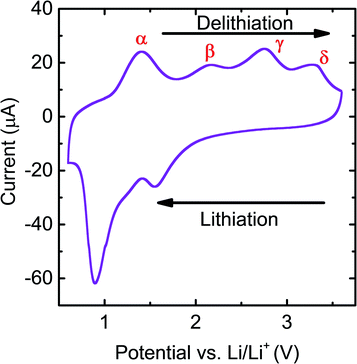 | ||
| Fig. 1 Cyclic voltammogram for an RuO2/LiPF6/Li cell obtained at a scan rate of 0.5 mV s−1 between 0.6 V and 3.6 V. The rationale for the peak labels is explained in the main text. | ||
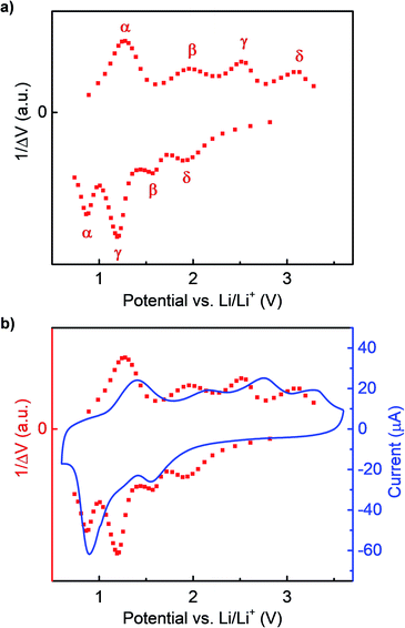
In Fig. 1, the shoulder on the main lithiation peak was tentatively identified as corresponding to an independent reaction β. To confirm this, GITT tests were carried out. During GITT tests, the equilibrium voltages of materials at specific states of charge can be obtained after long relaxation steps, minimizing the influence of kinetic effects. When the differences in the state of charge Δx between two consecutive steps are kept the same, a small change in the corresponding equilibrium voltage ΔV indicates that a reaction has occurred. Peaks in plots of 1/ΔV vs. V are therefore related to peaks seen in CV curves. However, because relaxation is allowed in GITT tests, kinetic effects that can cause overlap of peaks in CV curves are reduced.
The 1/ΔV vs. voltage curves extracted from GITT tests in a Li/RuO2 cell are shown in Fig. 2a, and a direct comparison with a CV curve is shown in Fig. 2b. Here it can be clearly seen that the same four delithiation peaks appear in both the GITT and CV plots. However, the GITT results clearly show four peaks during lithiation rather than three in the CV plot, confirming that the shoulder labeled β in the CV plot results from a distinct reaction seen at about 1.6 V in the GITT plot and that the large peak at about 0.8 V in the CV plot is composed of two overlapping peaks that can be clearly distinguished in the GITT plot, at about 0.9 V and 1.3 V.
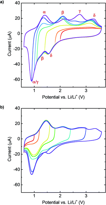
Having confirmed that the same number of reactions occur during lithiation and delithiation, we now use CV curves to associate the lithiation peaks seen in the lithiation curve with the corresponding peaks in the delithiation curve. We performed CV scans with the same upper cutoff voltage (3.6 V) but with different lower cutoff voltages (Fig. 3a). We also performed CV scans with the same lower cutoff voltage (0.6 V) but with different upper cutoff voltages (Fig. 3b). The results are summarized in Fig. 3a and b, respectively.
As seen in Fig. 3a, when the lower cutoff voltage is 2.0 V (red) and 1.8 V (orange), before the first lithiation peak at around 1.6 V, no obvious delithiation peak exists. When the lower cutoff voltage is further decreased to 1.4 V, which is between the first lithiation peak and the shoulder at around 1.3 V, a delithiation peak appears at around 3.2 V. This shows that the lithiation peak at 1.6 V and the delithiation peak at 3.2 V correspond to the same reaction. When the lower cutoff voltage is further decreased to 1.1 V (green), after the shoulder β, a second delithiation peak appears at around 2.0 V, which indicates that these peaks correspond to the same reaction. Finally, when the lower cutoff voltage was decreased to 1.0 V (azure), 0.9 V (blue) and 0.6 V (violet), we observe the appearance of two delithiation peaks at around 1.4 V and around 2.75 V. That two delithiation peaks appear for this range of cutoff voltages is consistent with the fact that the lithiation peak at around 0.8 V in the CV curve was found to correspond to two peaks in the GITT curves.
These relationships are confirmed using CV scans with different upper cutoff voltages, shown in Fig. 3b. The lithiation peak at 0.8 V did not appear until the upper cutoff voltage was increased to 1.6 V (yellow), and thus this peak was identified as associated with reaction α. The lithiation peak at 1.4 V appeared only after the upper cutoff voltage was increased to 2.4 V (cyan), and thus this peak was identified as associated with reaction β. Then, when the upper cutoff voltage was set at 3.0 V (blue), the intensity of the lithiation peak at 0.8 V increased significantly, indicating that this peak is also associated with reaction γ. Finally, for the fully delithiated sample (purple), the lithiation peak at around 1.6 V appeared, which implies that this peak is associated with reaction δ.
To distinguish between the two overlapping low-voltage lithiation peaks, GITT scans with different lower cutoff voltages were performed, and the corresponding 1/ΔV vs. voltage curves are shown in Fig. S9.† These results show that during lithiation, the reaction corresponding to γ occurs at a higher voltage than that of reaction α.
In summary, using GITT scans and CV scans with different lower cutoff and upper cutoff voltages, we confirmed that the lithiation CV peak at around 1.6 V corresponds to the delithiation peak at around 3.2 V, and the lithiation shoulder at around 1.3 V corresponds to the delithiation peak at around 2.0 V. The lithiation CV peak at around 0.8 V is a combination of two reaction peaks corresponding to the delithiation peaks at 1.4 V and 2.75 V. When the kinetic effects that cause overlapping peaks associated with the α and γ during lithiation were eliminated in GITT experiments, the lithiation reaction corresponding to the delithiation peak at 2.75 V is found to occur at a higher voltage than the reaction corresponding to the delithiation peak at 1.4 V. These relationships between the delithiation and lithiation peaks have been indicated by the labels in Fig. 2a and 3a.
In addition, it can be concluded from GITT cycle curves (Fig. S1†) and the 1/ΔV vs. voltage curve (Fig. 2a) that reaction γ contributed the most to the large voltage hysteresis of RuO2 during cycling. The hysteresis reached a magnitude of about 1.2 V, even when a relaxation time of 1.5 hours was used between steps.
3.2. Cross sectional transmission electron diffraction
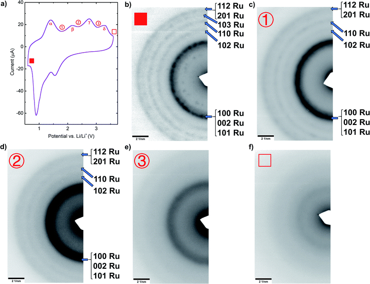
After determining the correspondence between lithiation and delithiation reactions shown in CV curves and deconvolving kinetic effects that lead to overlapping peaks using both GITT and CV experiments, ex situ characterizations using SAED, XPS and Raman spectroscopy on cycled thin film RuO2 samples were carried out. All samples were cycled at 0.5 mV s−1 until their cyclic voltammograms became stable. Different samples were then cycled at the same rate and stopped between different reaction peaks during the delithiation process, at the voltages ①, ② and ③ shown in Fig. 4a.Electron diffraction patterns (EDPs) were obtained from samples that were lithiated to the same lower cutoff voltage 0.6 V and then delithiated to the different voltages indicated in Fig. 4a, 1.8 V, 2.3 V, 3.0 V, and 3.6 V, corresponding to ①, ②, ③, and □, respectively. The radial average intensity functions for each case can be found in Fig. S4.† Diffraction rings that can be indexed to Ru are observed in the fully lithiated sample (■), as shown in Fig. 4b, and the fully delithiated RuO2 (□) is amorphous, as indicated by the broad halo seen in Fig. 4f. These results are consistent with previous in situ TEM studies.19 However, the (111) ring for Li2O was missing for the lithiated sample (■). This could be due to the high reactivity of Li2O as the fabrication of ex situ TEM samples inevitably included exposure to ambient, during which Li2O was likely to quickly degrade. For the sample delithiated to the intermediate state ①, after the first delithiation reaction α, all Ru rings are still present (Fig. 4c and S4†), though with fewer detectable individual diffraction spots and with more diffuse rings, suggesting that the Ru grain size has decreased.32 After delithiation to state ②, a voltage higher than required for the second delithiation reaction β, Ru rings still exist (Fig. 4d and S4†). Finally, after delithiation to a voltage above the delithiation peak γ, all Ru rings are missing except for a very weak remnant of the Ru (200) ring (Fig. 4e and S4†). These results show that metallic Ru forms in films lithiated to 0.6 V and remains present during delithiation to voltages higher than those of the α and β peaks, and is substantially reduced only at voltages above those associated with the γ reaction. Metallic Ru is presumably consumed in the conversion reaction to form RuO2. At a voltage above that associated with the reaction δ, the fourth delithiation peak, the film is amorphous and is presumably fully converted to RuO2.
3.3. X-ray photoelectron spectroscopy
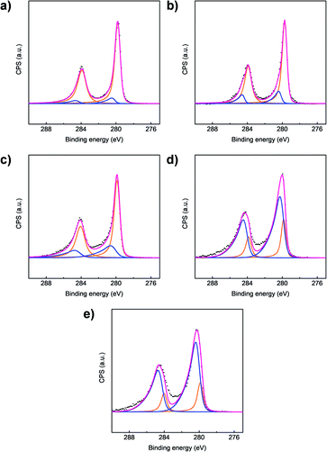
To support our findings from the EDPs, ex situ X-ray photoelectron spectra of Ru 3d orbitals for all samples were acquired and are shown in Fig. 5, with curves fitted for a mixture of metallic Ru metal and RuO2.33 At the beginning, when the film was fully lithiated at 0.6 V (Fig. 5a), the spectrum is dominated by metallic Ru, with only a small fraction of the Ru involved in bonding with O. This shows that during lithiation, RuO2 is converted to Ru metal, presumably through a reaction to form Li2O. Metallic Ru continues to be the dominant form of Ru through the first and second delithiation peaks (Fig. 5b and c). It is only after the third delithiation reaction γ (Fig. 5d), that RuO2 begins to dominate. This change suggests that the third delithiation peak γ is associated with the reaction of metallic Ru with Li2O to form RuO2. These findings are consistent with the EDP results. In addition, the RuO2/Ru metal ratio after peak δ was slightly higher than that before peak δ, which implies that there is a change of oxidation state during peak δ.3.4. Raman spectroscopy
Raman spectroscopy was also carried out to investigate the reactions that occur during delithiation, and by inference, lithiation. Data are shown in Fig. 6a, with the lowest curve corresponding to a sample in the fully lithiated state (0.6 V), and the ascending sequence of curves corresponding to samples that were delithiated to increasing voltages (as indicated in Fig. 4a). A peak is observed at about 240 cm−1 for all samples. The origin of this peak is unclear but it appears to minimally change at different stages of delithiation. This peak was therefore used as a reference peak for comparisons of the intensity of other peaks for samples delithiated to different voltages.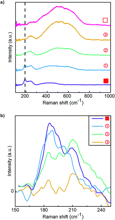 | ||
| Fig. 6 (a) Raman spectra for samples lithiated to 0.6 V, lower curve, and delithiated to different states (see Fig. 4a). (b) Raman spectra of samples at different lithiated states (■, ①, ② and ③), between 150 cm−1 and 250 cm−1, after subtraction of the Raman spectrum of the fully delithiated sample (□). | ||
The peak at a Raman shift of around 191 cm−1 is associated with metallic Ru.34 To confirm this, we obtained a separate Raman spectrum for a 10 nm-thick single crystal Ru film, Fig. S5,† for which a very strong peak at 191 cm−1 was seen. To focus on the intensity of this peak as a function of the degree of delithiation, the contribution from the peak at 240 cm−1 was minimized by subtracting the Raman spectrum of a fully delithiated sample (□), in which no metallic Ru exists, from the spectra of samples delithiated to different extents (■, ①, ② and ③). The results between 150 cm−1 and 250 cm−1 are shown in Fig. 6b. As the sputtered RuO2 films were delithiated, the peak at 191 cm−1 remained sharp after the first delithiation peak α (①). This peak became a bit weaker but broader after the second delithiation peak β (②), which indicates that the average grain size of the metallic Ru was smaller.35 After the third delithiation peak γ (③), the Raman peak at about 191 cm−1 mostly disappears, showing that the amount of metallic Ru decreased significantly during the reaction γ.
As the degree of delithiation is increased, a collection of peaks develop between 400 cm−1 and 700 cm−1, which are thought to be associated with amorphous RuO2,36 as the Raman spectrum of single crystal RuO2 consists of three peaks at 528, 646 and 716 cm−1. The relative intensity of these Raman peaks increased most significantly in association with CV peak γ (going from ② to ③), which suggests that the amount of RuO2 significantly increases during this reaction. These findings are consistent with the conclusions drawn based on EDP and XPS results.
3.5. Surface morphology and chemistry
In addition to the above characterizations, SEM and optical microscope images were captured and are shown in the ESI section as Fig. S6 and S7.† The surface of the electrode was observed to be covered by a layer before the delithiation peak β (for samples ■ and ①) but this layer was mostly removed after peak β (for samples ②, ③ and □). These results suggest that during delithiation, reaction β involves the decomposition of a surface layer.Ex situ energy dispersive X-ray spectroscopy (EDS) analysis also supports this hypothesis. Atomic percentages calculated using spectra collected from surfaces of the samples are listed in Table 1 (carbon not included). Before reaction β (samples ■ and ①), a large amount of F was found on the surface. After reaction β (samples ②, ③ and □), the concentration of F decreased substantially. F cannot originate from the pristine RuO2 films, ambient air or moisture, and any residual salt on the sample surface was rinsed off using solvent before observations were made. However, F is commonly found within SEI films for electrolytes containing LiPF6.15,41,42 These results suggest that the decomposed surface layer was an SEI layer on RuO2.
| Sample | Ru | O | F | P |
|---|---|---|---|---|
| ■ | 10.8 | 34.8 | 41.1 | 2.1 |
| ① | 17.8 | 15.1 | 59.8 | 1.9 |
| ② | 30.8 | 47.2 | 15.6 | 0 |
| ③ | 27.2 | 72.8 | 0 | 0 |
| □ | 23.3 | 66.00 | 4.8 | 0 |
3.6. In situ EIS
To further test this hypothesis, in situ EIS measurements were carried out and the results are summarized in Fig. 7. All the EIS measurements were carried out on freshly deposited thin-film RuO2 samples after ten CV cycles. From Fig. 7, it is seen that before the second delithiation peak β (samples ■ and ①), an extra arc exists in the high-frequency range (>50 Hz, small Re(Z)). This arc disappeared after peak β, (samples ②, ③ and □).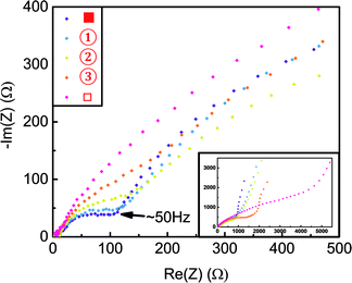 | ||
| Fig. 7 Nyquist plots of the potentiostatic impedance of different delithiated samples. The inset shows the entire dataset. | ||
This also suggests that the second delithiation peak β is related to the decomposition of the observed surface layer. As previous studies have revealed that a high-frequency (>30 Hz) arc is often associated with SEI layers on the surfaces of other electrode materials,37–40 this in situ result further supports the hypothesis that the delithiation peak β can be attributed to the decomposition of an surface layer.
3.7. PITT tests
PITT tests were performed within the voltage range of the conversion reaction γ (2–3 V) to study its kinetic behavior. Part of the PITT data is shown in Fig. 8 and the complete data from 2 V to 2.95 V can be found in Fig. S10.† The black curves show the current as a function of time after each voltage step, and the blue lines show the applied voltages during each step. As can be seen in Fig. 8, the current during each step decreases monotonically without a local maximum. This not only applies to the data shown in the figure, but also to data collected for various step sizes, holding times and voltage ranges.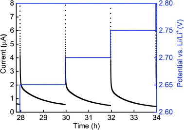 | ||
| Fig. 8 Current and voltage as a function of time during PITT test of a RuO2/LiPF6/Li cell. The steps shown are 2.65 V, 2.70 V and 2.75 V. | ||
PITT data can be used to distinguish between diffusion-limited reactions and phase-transition-limited reactions.43–45 When the reaction is diffusion-limited, the current decays monotonically during each voltage step. In contrast, when the reaction is phase-transition-limited, the current first decays, then increases and reaches a maximum, and finally decays again.
The monotonic decay observed during PITT measurements of RuO2 in the voltage range associated with the CV peak for γ suggests that the conversion reaction is diffusion-limited, not limited by the phase-transition. To characterize the length scale over which these diffusive processes occurred, CV scans of samples with different thicknesses were also performed (Fig. S3†). The positions of all four lithiation and delithiation peaks did not shift significantly even when the thickness was doubled, suggesting that the rate-limiting diffusive processes operate at length-scales that are small compared to the film thickness, and that they occur uniformly through the film thickness.
3.8. Discussion
During delithiation, reaction α happens first. Ru metal was found both before and after this reaction. Previous studies of the reactions that occurred during the first lithiation of pristine crystalline RuO2 have indicated that during the late stages of lithiation, excess Li can be stored between nanosized Ru and Li2O phases.21,23,24 Thus, we propose that reaction α is:| Excess Li in Ru/Li2O mixture → Li (counter electrode) + Ru/Li2O mixture. |
This is consistent with the smaller overpotential shown in the CV curve, as the desorption of Li doesn't involve chemical reactions and is kinetically easier.
The nature of the second delithiation reaction β is not as clear as that of the other reactions. As discussed above, ex situ microscopy shows clear evidence of a surface layer when films are lithiated to voltages below the β peak, and that this layer is not present on films that have been delithiated beyond the β peak. This surface layer might be the result of air exposure. However, in situ EIS measurements also show evidence for reversible formation of a surface layer in the voltage ranges associated with the β reaction. Also, EDS analysis of the layers shows a high level of F. These results suggest that reaction β might be associated with reversible formation of an SEI layer. If this is the case, reaction β would be:
| SEI (Li) → Li (counter electrode) + electrolyte |
This is consistent with the GITT/CV results, in which the sequence of lithiation reactions (α → γ → β → δ) is different from the sequence of delithiation reactions (α → β → γ → δ), which implies that the delithiation reaction β was independent of the other reactions.
As Ru metal was present before the third delithiation reaction γ but not after, we propose that the reaction corresponding to this peak involves the oxidation of Ru metal:
| 2Li2O + Ru → LixRuO2 + (4 − x)Li (counter electrode). |
This can also account for the fact that reaction α follows reaction γ during lithiation, as the small clusters of Ru and Li2O only form when the conversion reaction γ happens, during which excess Li can diffuse and reside between these phases.
Finally, given earlier studies of shallow lithiation of powder-based amorphous RuO2,17,18 we suggest that the change in oxidation state indicated by the slight shift of Ru 3d peaks in XPS spectra is associated with reaction peak δ. That is, Li alloys with amorphous RuO2 and forms an amorphous LixRuO2 phase, so that the reaction leading to the fourth delithiation peak δ would be:
| LixRuO2 → RuO2 + xLi (counter electrode). |
Given the correspondence between lithiation and delithiation reactions that was determined from CV/GITT tests, the sequence of reactions during lithiation (from high to low voltages) would therefore be:
| RuO2 + xLi (counter electrode) → LixRuO2 | (1) |
| Li (counter electrode) + electrolyte → SEI (Li) | (2) |
| LixRuO2 + (4 − x) Li (counter electrode) → 2Li2O + Ru | (3) |
| Li (counter electrode) + Ru/Li2O mixture → excess Li in Ru/Li2O mixture | (3′) |
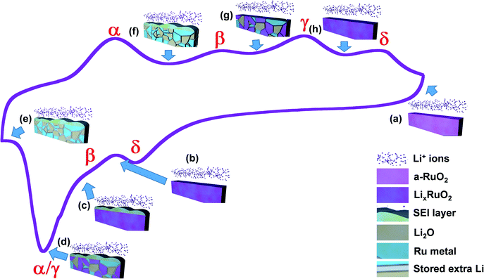
The proposed sequence for phase evolution during both lithiation and delithiation of RuO2 is summarized in Fig. 9.
By determining the reactions that occur during lithiation and delithiation of amorphous RuO2 thin films, it is concluded that the large voltage hysteresis of the conversion reaction contributes the most to the overall large voltage hysteresis, which significantly reduces the cycling energy efficiency. The conversion reaction during delithiation involves three kinetic sub-steps: nucleation of a new phase, LixRuO2, at the interfaces between Ru and Li2O clusters, local diffusion of O or Ru during growth of the new phase, and long-range diffusion of Li through the thin film. PITT results suggest that the nucleation and growth of the new phase is not the rate-limiting step. Moreover, the CV curves of RuO2 samples with different thicknesses (Fig. S3†) show no significant shift of reaction peak γ, although the thickness was more than doubled (from 160 nm to 400 nm). This implies that long-range diffusion of Li through the film is not the cause of the large voltage hysteresis. Consequently, the large voltage hysteresis of the conversion reaction is most likely due to local diffusion of O or Ru atoms.
4. Conclusions
Using a range of electrochemical and structural characterizations of multiply-cycled RuO2 films, we show that four reactions occur during lithiation: formation of amorphous LixRuO2 by insertion of Li into amorphous RuO2, formation of an SEI layer, a conversion reaction to form Li2O and Ru metal from LixRuO2, and insertion of metallic Li between nanosized Ru and Li2O particles. The same four reactions occur during delithiation, but not simply in reverse order. First Li is removed from between Ru and Li2O particles, the SEI layer that was formed during lithiation then reversibly dissociates, Ru and Li2O are then converted to LixRuO2 and Li is removed from LixRuO2 to form RuO2.The largest portion of the Li capacity of RuO2 electrodes is associated with the conversion reaction, and the potentials at which Li2O and Ru form from LixRuO2 during lithiation and at which the reverse reaction occurs during delithiation are separated by about 1.2 V in galvanostatic intermittent titrations. This leads to a hysteretic effect that causes poor cycling efficiency for RuO2, and by analogy, likely for other conversion electrode materials. We suggest that the high overpotentials required for these reactions are due to kinetic limitations associated with short range diffusion.
The methodologies used here for analysis of reactions that lead to high capacities in thin film electrodes, especially conversion-reaction electrodes, provide useful complements to analyses of powder-based materials. These studies also provide an important background for ongoing efforts to improve performance of RuO2 electrodes for thin film batteries.
Conflicts of interest
There are no conflicts to declare.Acknowledgements
This research was supported by the Skoltech Center for Electrochemical Energy Storage as part of the Skoltech-MIT program. It was also supported by the National Research Foundation, Prime Minister's Office, Singapore, under its Campus for Research Excellence and Technological Enterprise (CREATE) program, through the Singapore-MIT Alliance for Research and Technology (SMART), Low Energy Electronic Systems (LEES) Interdisciplinary Research Group (IRG). We thank S. Ezzat and K. S. Coffey of the University of Central Florida for single-crystal Ru films. We are also grateful for helpful discussions with J. Miao, B. Wang, M. J. Chon and A. Weathers. This work made use of the MRL MRSEC Shared Experimental Facilities at MIT, supported by the National Science Foundation under award number DMR-1419807.Notes and references
- S. Ornes, Proc. Natl. Acad. Sci. U. S. A., 2016, 113, 11059–11060 CrossRef CAS.
- V. Aravindan, Y.-S. Lee and S. Madhavi, Adv. Energy Mater., 2015, 5, 1402225 CrossRef.
- M. H. Oh, T. Yu, S.-H. Yu, B. Lim, K.-T. Ko, M.-G. Willinger, D.-H. Seo, B. H. Kim, M. G. Cho, J.-H. Park, K. Kang, Y.-E. Sung, N. Pinna and T. Hyeon, Science, 2013, 340, 964–968 CrossRef CAS.
- J. Jiang, Y. Li, J. Liu, X. Huang, C. Yuan and X. W. D. Lou, Adv. Mater., 2012, 24, 5166–5180 CrossRef CAS.
- S. M. Yuan, J. X. Li, L. T. Yang, L. W. Su, L. Liu and Z. Zhou, ACS Appl. Mater. Interfaces, 2011, 3, 705–709 CrossRef CAS.
- S. H. Yu, S. H. Lee, D. J. Lee, Y. E. Sung and T. Hyeon, Small, 2016, 12, 2146–2172 CrossRef CAS.
- A. S. Hassan, K. Moyer, B. R. Ramachandran and C. D. Wick, J. Phys. Chem. C, 2016, 120, 2036–2046 CrossRef CAS.
- M. A. Lowe, J. Gao and H. D. Abruña, J. Mater. Chem. A, 2013, 1, 2094–2103 RSC.
- P. G. Bruce, B. Scrosati and J. M. Tarascon, Angew. Chem., Int. Ed., 2008, 47, 2930–2946 CrossRef CAS.
- F. Wu and G. Yushin, Energy Environ. Sci., 2017, 10, 435–459 RSC.
- M. Keppeler and M. Srinivasan, ChemElectroChem, 2017, 4, 2727–2754 CrossRef CAS.
- D. Perego, J. S. T. Heng, X. Wang, Y. Shao-Horn and C. V. Thompson, Electrochim. Acta, 2018, 283, 228–233 CrossRef CAS.
- J. Zhu, K. B. Yeap, K. Zeng and L. Lu, Thin Solid Films, 2011, 519, 1914–1922 CrossRef CAS.
- J. Zhu, K. Zeng and L. Lu, Metall. Mater. Trans. A, 2013, 44, 26–34 CrossRef CAS.
- P. Balaya, H. Li, L. Kienle and J. Maier, Adv. Funct. Mater., 2003, 13, 621–625 CrossRef CAS.
- T. Ohzuku, J. Electrochem. Soc., 1990, 137, 3004 CrossRef CAS.
- D. Muñoz-Rojas, M. Casas-Cabanas and E. Baudrin, Solid State Ionics, 2010, 181, 536–544 CrossRef.
- O. Delmer, P. Balaya, L. Kienle and J. Maier, Adv. Mater., 2008, 20, 501–505 CrossRef CAS.
- K. E. Gregorczyk, Y. Liu, J. P. Sullivan and G. W. Rubloff, ACS Nano, 2013, 7, 6354–6360 CrossRef CAS.
- M. Mao, A. Nie, J. Liu, H. Wang, S. X. Mao, Q. Wang, K. Li and X.-X. Zhang, Nanotechnology, 2015, 26, 125404 CrossRef.
- A. S. Hassan, A. Navulla, L. Meda, B. R. Ramachandran and C. D. Wick, J. Phys. Chem. C, 2015, 119, 9705–9713 CrossRef CAS.
- Y. Y. Hu, Z. Liu, K. W. Nam, O. J. Borkiewicz, J. Cheng, X. Hua, M. T. Dunstan, X. Yu, K. M. Wiaderek, L. S. Du, K. W. Chapman, P. J. Chupas, X. Q. Yang and C. P. Grey, Nat. Mater., 2013, 12, 1130–1136 CrossRef CAS.
- Y. Kim, S. Muhammad, H. Kim, Y. H. Cho, H. Kim, J. M. Kim and W. S. Yoon, ChemSusChem, 2015, 8, 2378–2384 CrossRef CAS.
- E. Bekaert, P. Balaya, S. Murugavel, J. Maier and M. Ménétrier, Chem. Mater., 2009, 21, 856–861 CrossRef CAS.
- J. Cabana, L. Monconduit, D. Larcher and M. R. Palacín, Adv. Mater., 2010, 22, 170–192 CrossRef.
- Y. Oumellal, A. Rougier, G. A. Nazri, J. M. Tarascon and L. Aymard, Nat. Mater., 2008, 7, 916–921 CrossRef CAS.
- F. Wang, R. Robert, N. A. Chernova, N. Pereira, F. Omenya, F. Badway, X. Hua, M. Ruotolo, R. Zhang, L. Wu, V. Volkov, D. Su, B. Key, M. Stanley Whittingham, C. P. Grey, G. G. Amatucci, Y. Zhu and J. Graetz, J. Am. Chem. Soc., 2011, 133, 18828–18836 CrossRef CAS.
- L. Li, R. Jacobs, P. Gao, L. Gan, F. Wang, D. Morgan and S. Jin, J. Am. Chem. Soc., 2016, 138, 2838–2848 CrossRef CAS.
- I. Ullah, Y. Xu, W. ur Rehman, Y. Zhang, C. Wang and L. Li, J. Alloys Compd., 2019, 802, 591–599 CrossRef CAS.
- W. Dreyer, J. Jamnik, C. Guhlke, R. Huth, J. Moškon and M. Gaberšček, Nat. Mater., 2010, 9, 448–453 CrossRef CAS.
- V. A. Sethuraman, V. Srinivasan and J. Newman, J. Electrochem. Soc., 2013, 160, A394–A403 CrossRef CAS.
- A. L. Patterson, Phys. Rev., 1939, 56, 978–982 CrossRef CAS.
- D. J. Morgan, Surf. Interface Anal., 2015, 47, 1072–1079 CrossRef CAS.
- M. Lewandowski, B. Scheibe, T. Vasileiadis, N. Michalak, Z. Miłosz, R. Ranecki, S. Mielcarek, T. Luciński and S. Jurga, Surf. Coat. Technol., 2015, 271, 87–91 CrossRef CAS.
- I. H. Campbell and P. M. Fauchet, Solid State Commun., 1986, 58, 739–741 CrossRef CAS.
- S. Y. Mar, C. S. Chen, Y. S. Huang and K. K. Tiong, Appl. Surf. Sci., 1995, 90, 497–504 CrossRef CAS.
- S. S. Zhang, K. Xu and T. R. Jow, Electrochim. Acta, 2006, 51, 1636–1640 CrossRef CAS.
- L. Wang, J. Zhao, X. He, J. Gao, J. Li, C. Wan and C. Jiang, Int. J. Electrochem. Sci., 2012, 7, 345–353 CAS.
- M. D. Levi, J. Electrochem. Soc., 1999, 146, 1279 CrossRef CAS.
- R. Yazami and D. Guérard, J. Power Sources, 1993, 43, 39–46 CrossRef CAS.
- A. Wang, S. Kadam, H. Li, S. Shi and Y. Qi, npj Comput. Mater., 2018, 4, 15 CrossRef.
- N. Takenaka, Y. Suzuki, H. Sakai and M. Nagaoka, J. Phys. Chem. C, 2014, 118, 10874–10882 CrossRef CAS.
- J. Miao, B. Wang and C. V. Thompson, Phys. Rev. Mater., 2020, 4, 1–10 Search PubMed.
- N. Meethong, Y. H. Kao, W. C. Carter and Y. M. Chiang, Chem. Mater., 2010, 22, 1088–1097 CrossRef CAS.
- F. Y. Fan, W. C. Carter and Y. M. Chiang, Adv. Mater., 2015, 27, 5203–5209 CrossRef CAS.
Footnote |
| † Electronic supplementary information (ESI) available. See DOI: 10.1039/d0ta06428a |
| This journal is © The Royal Society of Chemistry 2020 |

