
 Open Access Article
 This Open Access Article is licensed under a
 Creative Commons Attribution 3.0 Unported Licence
α-Bi2Sn2O7: a potential room temperature n-type oxide thermoelectric†
Warda
Rahim
 *ab,
Jonathan M.
Skelton
c and
David O.
Scanlon
abd
*ab,
Jonathan M.
Skelton
c and
David O.
Scanlon
abd
aDepartment of Chemistry, University College London, 20 Gordon Street, London, WC1H 0AJ, UK. E-mail: warda.rahim.18@ucl.ac.uk; d.scanlon@ucl.ac.uk
bThomas Young Centre, University College London, Gower Street, London, WC1E 6BT, UK
cDepartment of Chemistry, University of Manchester, Oxford Road, Manchester, M13 9PL, UK
dDiamond Light Source Ltd., Diamond House, Harwell Science and Innovation Campus, Didcot, Oxfordshire OX11 0DE, UK
First published on 22nd July 2020
Abstract
Interest in oxide thermoelectrics has been building due to their high thermal stability and earth-abundant constituent elements. However, the thermoelectric efficiency of flagship oxide materials remains comparatively low, and most materials only reach the maximum figure of merit, ZT, at very high temperatures, above those where the majority of low-grade industrial heat is emitted. It is important to identify thermoelectrics with high conversion efficiency closer to room temperature, particularly for lower-temperature applications such as in domestic heating, consumer electronics and electric vehicles. One of the main factors limiting the efficiency of oxide thermoelectrics is their large lattice thermal conductivities, which has inspired research into more structurally complex materials. In this study, we apply first-principles modelling to assess the low-temperature polymorph of Bi2Sn2O7 (α-Bi2Sn2O7) as a potential thermoelectric material, due to its complex crystal structure, which should suppress phonon transport, and the presence of Bi p and Sn s states in the conduction band, which should yield high electrical conductivity when donor (n) doped. Lattice-dynamics calculations using third-order perturbation theory predict an ultralow room-temperature lattice thermal conductivity of 0.4 W m−1 K−1, the lowest ever predicted for an oxide material, and suggest that nanostructuring to a grain size of 5 nm could further decrease this to 0.28 W m−1 K−1. The ultralow lattice thermal conductivity gives α-Bi2Sn2O7 a maximum ZT of 0.36 at 385 K (0.46 with nanostructuring), which is the highest low-temperature value predicted for an oxide thermoelectric. Most importantly, our analysis highlights the relationship between the structural complexity, the chemical nature of the cation, and the short phonon lifetimes, and thus provides guidelines for identifying other novel high-performance oxide thermoelectrics.
1 Introduction
The growing global demand for renewable energy sources and the major environmental challenges posed by continued greenhouse gas emissions have made it vital to find new means to improve the efficiency of energy-intensive processes. Some 60% of global energy is wasted as heat, and thermoelectric power provides a means to recover this waste as useful electrical energy. Thermoelectrics can be used either for active cooling, consuming electrical energy to transport heat against a temperature gradient, or for power generation by extracting electrical energy from a temperature gradient.1 At present, large-scale thermoelectric power generation is not feasible due to the scarcity of the constituent elements in flagship materials such as Bi2Te3 and the limited efficiency of more sustainable alternatives. Despite huge investment and research into the development of new thermoelectrics, the field has not made a large amount of progress in the last 50 years.2The efficiency of a thermoelectric device is determined by the dimensionless figure of merit, ZT, defined as:
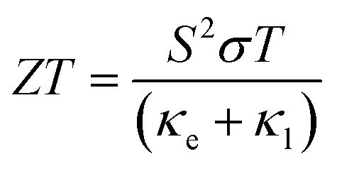 | (1) |
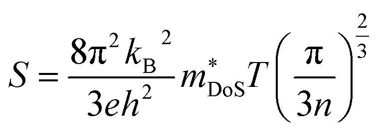
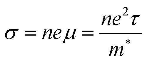
The properties in the ZT equation are intricately linked, which makes optimising ZT a difficult task. Maximising ZT requires the thermopower S2σ to be maximised and the total thermal conductivity κ from both the charge carriers and the lattice vibrations (phonons) to be minimised. A high Seebeck coefficient S results from a high density of states effective mass,  , and low carrier concentration as shown in eqn (2).
 | (2) |
 | (3) |
| κe = LσT | (4) |
Recently, SnSe rose to the forefront of thermoelectric research due to its ultralow high-temperature lattice thermal conductivity of <0.5 W m−1 K−1 along the layering direction,5 highlighting the importance of low lattice thermal conductivity in achieving high ZT values. There has thus been a surge in studying complex ternary and quaternary structures for thermoelectric applications. Mass contrast due to multiple constituent elements, as well as the inevitable higher structural complexity, favours increased phonon scattering and leads to lower lattice thermal conductivity. Building upon this, several ternary and quaternary compounds with complex structures and incorporating heavy elements have been identified that have lower κl values compared to the industry standard Bi2Te3.6–10 Such complex structures often also have higher effective masses and thus high Seebeck coefficients.
For a material to be used in a thermoelectric module, where several TE materials are joined together in a couple, it is also important that the constituent elements are earth abundant and non-toxic. This provides another compelling reason to investigate oxide thermoelectrics, as they consist of chemically-inert and earth-abundant elements.11 For a practical TE device, the thermoelectric materials should ideally meet a target ZT of >1. Although the ZT values of some of oxide thermoelectrics exceed this threshold at high temperature, figures of merit at room temperature (300 K) are often <0.1. Materials with layered structures comprising two different layers stacked along one crystallographic axis have emerged as the most promising candidates for p-type oxide thermoelectrics. Some of the best-performing examples include NaxCoO2−δ, Ca3Co4O9 and Bi2Sr2Co2Oy, which have room-temperature ZT values of 0.036, 0.07, and 0.06 to 0.09, respectively.12–15 Among the n-type oxides, materials with the perovskite structure generally perform better than other structure types. This class includes SrTiO3 and CaMnO3, which upon doping have managed to attain maximum room temperature ZT values around 0.03 (ref. 16) and 0.05 (ref. 17–19) respectively. One of the main contributors to the low ZT values of these structures is their high thermal conductivity,20 which has also been established as a limiting factor in the thermoelectric performance of transparent conducting oxides.21 Various attempts at alloying, substitution and nanostructuring have been made to reduce κ within these structures,22,23 but have not been fruitful, with κ remaining larger than 1 W m−1 K−1 at room temperature.
In addition to good electronic and thermal transport properties, the “dopability”, refers to the carrier concentration limits which can be reached in a semiconductor,24 also plays a significant role in predicting device performance. In this work, we study the thermoelectric properties of α-Bi2Sn2O7, a complex ternary oxide with a pyrochlore-based structure, and a quantitative and accurate study of its dopability is important to fully gauge its potential as a good thermoelectric material. In principle, this can be achieved using first-principles defect calculations which may form part of future work.
Bi2Sn2O7 exists in three different polymorphic forms. The room temperature α form undergoes a first-order phase transition to a β structure at about 390 K, followed by a second-order phase transition to the γ polymorph above 900 K.25 The structure of the high-temperature γ polymorph is undisputed and is the standard cubic Fd![[3 with combining macron]](https://www.rsc.org/images/entities/char_0033_0304.gif) m pyrochlore structure, but there has been debate around the structures of the intermediate and room-temperature polymorphs. Lewis et al. resolved this controversy using an exhaustive and automated symmetry mode analysis approach wherein they generated a complete set of candidate structures between the parent γ-Bi2Sn2O7 and a lower symmetry P1 structure and refined each against combined neutron and high-resolution X-ray diffraction (XRD) data.26 Based on this, they suggested the first reliable structural model for the β phase, belonging to the Aba2 space group (41) with 176 atoms per unit cell, and a simplified model for the α phase belonging to the Cc spacegroup (9) with 88 atoms in the unit cell (Fig. 1). This is in contrast to the previous structural model of α-Bi2Sn2O7, which was in the Pc spacegroup (7) and has 352 atoms in the unit cell.27 Recently, using a theoretically-rigorous phonon mode-mapping approach, we elucidated the lowest energy polymorph of Bi2Sn2O7,28 and found it to be the new structural model of α (Cc) suggested by Lewis et al.26
m pyrochlore structure, but there has been debate around the structures of the intermediate and room-temperature polymorphs. Lewis et al. resolved this controversy using an exhaustive and automated symmetry mode analysis approach wherein they generated a complete set of candidate structures between the parent γ-Bi2Sn2O7 and a lower symmetry P1 structure and refined each against combined neutron and high-resolution X-ray diffraction (XRD) data.26 Based on this, they suggested the first reliable structural model for the β phase, belonging to the Aba2 space group (41) with 176 atoms per unit cell, and a simplified model for the α phase belonging to the Cc spacegroup (9) with 88 atoms in the unit cell (Fig. 1). This is in contrast to the previous structural model of α-Bi2Sn2O7, which was in the Pc spacegroup (7) and has 352 atoms in the unit cell.27 Recently, using a theoretically-rigorous phonon mode-mapping approach, we elucidated the lowest energy polymorph of Bi2Sn2O7,28 and found it to be the new structural model of α (Cc) suggested by Lewis et al.26
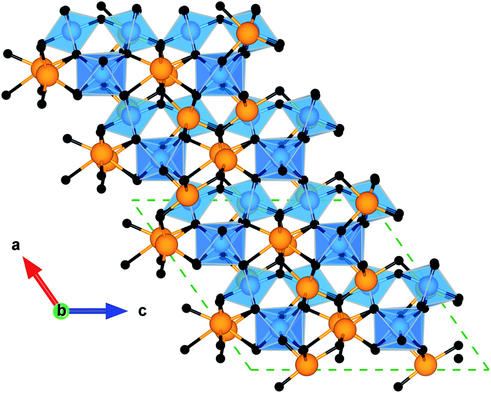 | ||
| Fig. 1 Crystal structure of α-Bi2Sn2O7. The view along the [010] plane is aligned along the SnO6 octahedra and highlights the disorder in the Bi atomic chains along the b axis. The atoms are coloured as follows: Bi – orange, Sn – blue, O and O′ – black. These images were generated using the VESTA software.29 | ||
The complex structure of α-Bi2Sn2O7 results from distortions of the high-symmetry γ polymorph. The pyrochlore structure comprises two oxide sublattices consisting of corner-sharing SnO6 octahedra and Bi4O′ tetrahedra. The interpenetration of these two sublattices results in a hexagonal bipyramidal BiO6O2′ coordination around the Bi atoms with six long equatorial Bi–O bonds and two short axial Bi–O′ bonds. As the temperature is reduced, γ-Bi2Sn2O7 changes progressively to the lower symmetry α structure, which involves minimal internal distortion of SnO6 octahedra and large correlated displacements of the Bi atoms.26,30 The distortion is driven by the 6s2 lone pair of electrons on Bi3+ ions and their tendency to prefer non-centrosymmetric coordination environments. In contrast to the eight-coordinate Bi atoms in the standard pyrochlore structure, this results in each Bi atom in α-Bi2Sn2O7 coordinating to five oxygen atoms, with the lone pair occupying its own distinct position. The lone pair effect results in this polymorph being the most thermodynamically stable form of Bi2Sn2O7.31
The recent structural solution of the room-temperature polymorph of Bi2Sn2O7 motivated us to study its thermoelectric properties. We anticipated, on the basis of its complex structure, the large number of atoms in the unit cell, and the presence of the stereochemically active lone pair, that it would likely have a low lattice thermal conductivity. The lone pair in SnSe was recently shown to introduce significant anharmonicity into the lattice dynamics,5 while the complex structure and large number of atoms should lead to a dense phonon dispersion and allow for multiple phonon scattering pathways, aided by the large mass contrast between the heavier Bi/Sn cations and lighter O anions. Furthermore, Bi2Sn2O7 should possess conduction band minimum (CBM) features consistent with many excellent conducting oxides containing post transition metal cations in their highest oxidation state, including ZnO,32 SnO2,33–36 In2O3,37 CdO38 and BaSnO3.39 In particular the presence of disperse Sn s states at the CBM is indicative of good carrier mobility, if effective donor doping can be achieved.
In this study, we show using first-principles calculations that the room temperature polymorph of Bi2Sn2O7 has an ultralow lattice thermal conductivity due to the presence of heavy metal cations, a complex structure, and the active Bi3+ lone pair. With suitable n-type doping, we predict it to have a high room-temperature ZT relative to other oxide thermoelectrics, highlighting how this strategy may serve as a new route to obtaining high ZT values in oxide materials.
2 Computational modelling
2.1 First-principles calculations
Calculations were performed using pseudopotential plane-wave density functional theory (DFT)40 as implemented in the Vienna Ab initio Simulation Package (VASP).41–44 The PBEsol functional,45 a variation of the Perdew–Burke–Ernzerhof (PBE) generalised-gradient approximation (GGA) functional46 revised for solids, was used, as this functional has consistently been shown to give structural properties and phonon frequencies in good agreement with experiment.47–51 The projector augmented-wave (PAW) method52 was used to represent the core electrons, treating Bi 5d106s26p3, Sn 4d105s25p2 and O 2s22p4 as valence states. Convergence testing using the primitive cell of α-Bi2Sn2O7 (44 atoms) suggested that a Γ-centered 3 × 3 × 2 k-point mesh and 500 eV plane-wave kinetic-energy cutoff were sufficient to converge the total energy to within 1 meV per atom and 3 meV per atom respectively (Fig. S1†). For the geometry optimisations the cutoff energy was increased to 650 eV to avoid Pulay stress,53 and the optimisation was deemed converged when the residual Hellmann–Feynman forces acting on the atoms were less than 10−4 eV Å−1.2.2 Electronic-structure and transport calculations
To calculate the electronic band structure and density of states, the screened Heyd–Scuseria–Ernzerhof hybrid functional (HSE06)54 was employed, as HSE06 is known to give band gaps in better agreement with experiment compared to PBEsol.55,56 HSE06 splits the exchange interaction into short range (SR) and long range (LR) components, and 25% of the PBE exchange energy is replaced with the exact Hartree–Fock exchange at short-range. Relativistic effects were modelled by explicit treatment of spin–orbit coupling (SOC) effects.57 The electronic band structure and density of states plots were produced using the open source Python package sumo.58Electronic transport properties were calculated using the semi-classical Boltzmann transport theory59,60 as implemented in the BoltzTraP code.61 BoltzTraP calculates transport coefficients using the constant relaxation time approximation (RTA), where the electron relaxation time τ is set to a single, isotropic value of 1 × 10⁻¹⁴ s. This method was chosen since calculating electronic relaxation times from first principles requires an explicit treatment of electron–phonon coupling; while this has been implemented in codes such as AMSET, it is computationally very demanding and thus not practical for low-symmetry structures with large unit cells. The code has previously been tested on a variety of systems and found to give results in good agreement with experiment.62–64 It uses a smoothed Fourier expansion to obtain an analytical expression for the band energies, based on the charge carriers responsible for transport being present within a narrow energy range due to a delta function-like Fermi broadening. The interpolated bands pass exactly through the calculated band energies, but outside of these points the derivatives at band crossings cannot be evaluated accurately. These calculations therefore require a dense k-point mesh to keep such errors localised so as not to significantly impact the calculated transport properties, and because the predicted transport properties are obtained as a summation over many Fermi surfaces. We therefore used a denser k-point mesh with 12 × 12 × 7 subdivisions, containing 285 k-points in the irreducible Brillouin zone, for these calculations. Using BoltzTraP, we obtain the electronic conductivity σ/τ, the Seebeck coefficient S, electronic thermal conductivity κe/τ, and the electronic power factor S2σ/τ as a function of temperature and carrier concentration. The ab initio predicted dimensionless figure of merit ZT is then predicted using these calculated electrical properties and calculated lattice thermal conductivity obtained as described below.
2.3 Lattice-dynamics calculations
Phonon dispersions, density-of-states (DoS) curves and other harmonic quantities were obtained from supercell finite-displacement phonon calculations using the Phonopy package65,66 with VASP as the force calculator. These were combined with third-order force constants to calculate phonon lifetimes perturbatively within the single-mode relaxation time approximation (SM-RTA) using the Phono3py package.67 The SM-RTA provides a closed-form solution to the linearised phonon Boltzmann transport equation (LBTE) which relates the macroscopic κl to a sum of contributions from individual phonon modes λ (eqn (5)):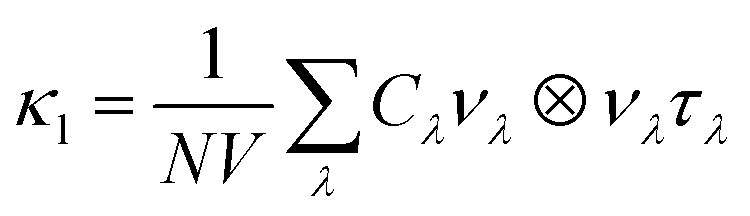 | (5) |
C λ and νλ are calculated within the harmonic approximation and assumed to be temperature independent. τλ are computed from the phonon linewidths Γλ as τλ = 1/(2Γλ). Γλ are computed from the imaginary part of the phonon self-energy, which is computed perturbatively based on the strengths of energy- and momentum-conserving three-phonon scattering processes.67
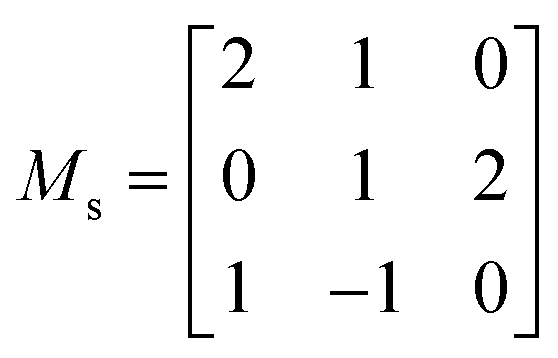
For the calculation of both the second- and third-order IFCs, we used the supercell finite-displacement method.68,69 To obtain the second-order IFCs, the 264 symmetry-inequivalent displacements were performed in a 264-atom cubic supercell expansion of the primitive cell, obtained using the supercell transformation matrix (Ms) shown below:
 | (6) |
This was found to be sufficient to converge the computed phonon dispersion (see Fig. S3†). Evaluation of the third-order IFCs requires pairwise atomic displacements to be performed in a chosen supercell, the number of which scales with the supercell size. As a compromise between accuracy and computational cost, the IFCs were calculated in the 88-atom conventional cell of α-Bi2Sn2O7, requiring a total of 69![[thin space (1/6-em)]](https://www.rsc.org/images/entities/char_2009.gif) 828 single-point calculations.
828 single-point calculations.
PBEsol was used for force calculations, as it has been shown to give a good description of lattice dynamics in semiconductors.47,48 The 650 eV kinetic-energy cutoff used for the geometry optimisations was also used for the force calculations, but we did not include an explicit treatment of SOC effects as in the electronic-structure calculations, as these are unlikely to affect the calculated phonon frequencies but would significantly increase the computational cost.70 The Γ-centred 3 × 3 × 2 k-point mesh used for the geometry optimisations was scaled appropriately for the supercell force calculations.
The phonon DoS was calculated by interpolating frequencies onto a uniform Γ-centered q-point mesh with 12 × 12 × 6 subdivisions. The phonon dispersion was evaluated by interpolating the frequencies to strings of q-points on a set of paths between the high-symmetry wavevectors in the phonon Brillouin zone.
Modal properties were evaluated in the reciprocal space of the conventional unit cell on a Γ-centered q-point mesh with 6 × 9 × 6 subdivisions, chosen based on explicit convergence tests (Fig. S4†), and the Brillouin zone integration was performed using the linear tetrahedron method.71–73
We also evaluated the pairwise contributions of other modes to the overall linewidths of each phonon mode. Due to the volume of data generated, this was performed using a smaller Γ-centered q-point mesh with 4 × 6 × 4 subdivisions, which yields κl values within 5–7% of the denser mesh used in the evaluation of other modal properties (Fig. S4†). Finally, to further investigate the microscopic origin of the phonon lifetimes, we calculated the averaged three-phonon interaction strengths and the two-phonon joint DoS describing the density of energy- and momentum-conserving scattering events as a function of frequency. As the former are very expensive to compute, they were therefore evaluated on a smaller Γ-centered mesh with 2 × 3 × 2 subdivisions, while the JDoS functions were evaluated using the same mesh used to calculate the other properties.
3 Results and discussion
3.1 Equilibrium geometry and electronic structure
The calculated equilibrium lattice constants for the primitive cell are listed along with experimental values in Table 1. We obtain excellent agreement between the theoretical and experimental geometries, with typical deviations of <1%.| a (Å) | b (Å) | c (Å) | α | β | γ | |
|---|---|---|---|---|---|---|
| PBEsol | 7.566 | 7.566 | 13.115 | 73.1° | 106.9° | 120.1° |
| Expt.26 | 7.582 | 7.582 | 13.144 | 72.7° | 107.3° | 120.4° |
| % Error | −0.2% | −0.2% | −0.2% | +0.6% | −0.4% | −0.2% |
The calculated electronic density of states (EDoS) is shown together with an expanded view of valence and conduction band edges in Fig. 2. The valence band maximum (VBM) is dominated by O 2p and Bi 6s states, with small contributions from Bi 6p and Bi 5d states. Between −1 and −4 eV below the VBM, the DoS mainly comprises O 2p, Sn 4d, Sn 5p and Bi 6p states, while between −4 and −6 eV the valence band is dominated by O 2p, Bi 6p, Sn 5s and Sn 5p states. The feature from −6 to around −8 eV consists of O 2p and Sn 5s states, while the feature at lower energies around −10 eV is formed of O 2p and Bi 6s states. The Bi 6s states undergo a bonding interaction with O 2p states at the bottom of the VB and an antibonding interaction at the top. These antibonding states are filled and thus form the VBM. In the distorted polymorph of Bi2Sn2O7, these states couple to Bi 6p and lead to the formation of an asymmetric electron density around the Bi atoms due to their stereochemically active 6s2 lone pair. This is consistent with the presence of Bi 6p states in the VBM, and a similar phenomenon arises in other post-transition metal oxides from the interaction of the metal s and p states mediated by the anion p states.74,75 On the other hand, the conduction band edge predominantly consists of Bi 6p and O 2p states, while in the rest of the conduction band we observe dominant contributions from Bi 6p, O 2p and Sn 5s states. The conduction band minimum (CBM) also contains small amounts of Sn 5s states, which would mix with Bi 6p and O 2p states to yield low electron effective masses at the Γ-point.
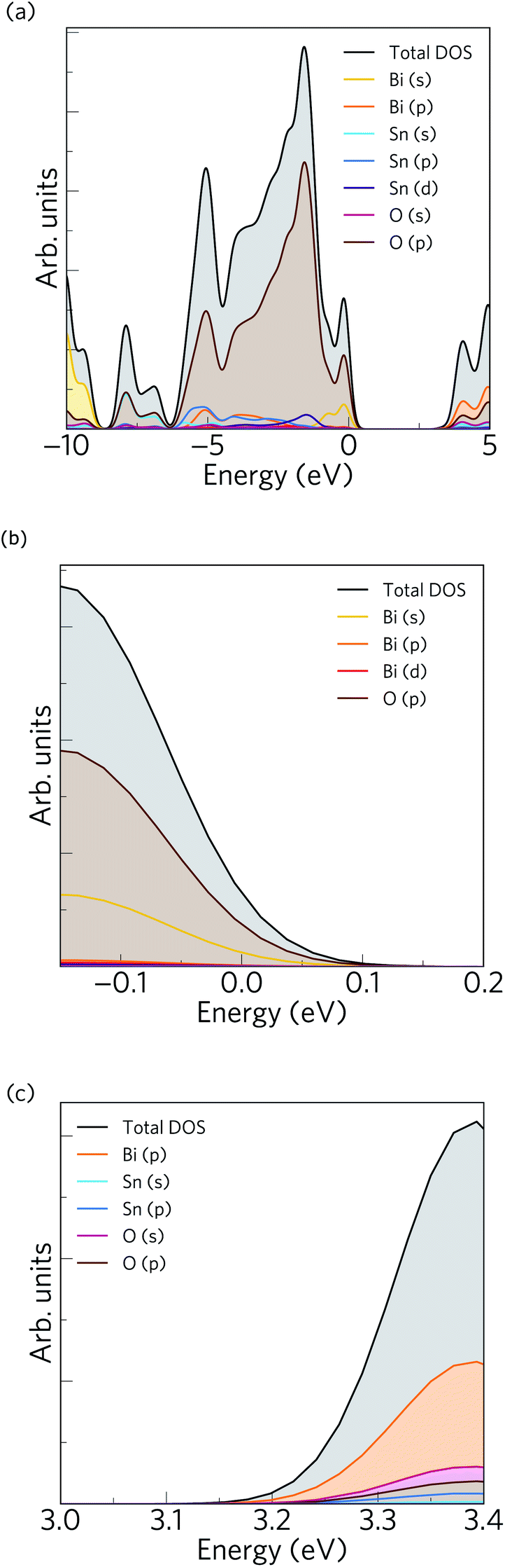 | ||
| Fig. 2 Electronic structure of α-Bi2Sn2O7. (a) Calculated total and projected electronic density of states obtained using HSE06 + SOC with the valence band maximum (VBM) at E = 0 eV. (b)/(c) Expanded views of the VBM and conduction band minimum (CBM). | ||
To validate our calculated electronic structure against experiment, we compared against the experimental valence band (VB) X-ray photoemission spectrum (XPS spectrum).75 The GALORE software package76 was used to simulate a VB photoelectron spectrum from our calculated electronic density of states. The photoionization cross section depends on the probe radiation, the orbital shapes and their energies, and to account for this GALORE uses the Gelius method77 to apply weightings to the atom-projected EDoS using the photoionization cross-sections formulated by Yeh and Lindau.78 For heavy elements, however, the valence s and p orbitals show relativistic effects, which are not taken into account in these calculated cross-sections, and which is thus likely to result in some deviation in the simulated and measured spectra. Nevertheless, overlaying the calculated and measured spectra (Fig. 3) shows excellent correspondence between the positions of features in the EDoS obtained from our optimised structure using hybrid DFT and the measured VB XPS spectrum.
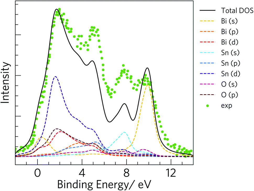 | ||
| Fig. 3 Simulated valence band (VB) X-ray photoelectron spectrum (XPS spectrum) obtained from the electronic density of states calculated using the HSE06 hybrid functional with spin–orbit corrections. The green markers show the experimental VB XPS spectrum for comparison.75 | ||
The electronic band structure of α-Bi2Sn2O7 in Fig. 4 indicates an indirect fundamental band gap of 3.47 eV and a direct gap of 3.51 eV. The interaction with Bi 6p states at the top of VB stabilises the s – p antibonding orbitals, resulting in an increased band gap compared to the high-temperature γ-Bi2Sn2O7 polymorph.31
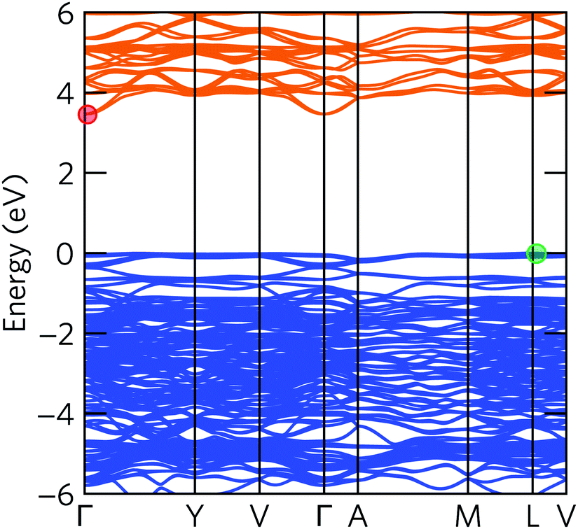 | ||
| Fig. 4 Electronic band structure of α-Bi2Sn2O7 calculated using the HSE06 hybrid functional with spin–orbit coupling. The valence and conduction bands are coloured blue and orange, respectively, and the valence-band maximum (VBM) is set to E = 0 eV. The VBM between L and V and the conduction-band minimum (CBM) between Γ and Y are marked with green and red circles, respectively. | ||
In our calculations, including explicit treatment of spin–orbit coupling (SOC) resulted in a band gap renormalisation of about 0.3 eV, which was mainly due to a lowering in energy of the CBM (Fig. S2†). This is due to the presence of Bi 6p states in the CBM and the scaling of the SOC correction as approximately Z4. Moreover, including SOC shifts the VBM from the high-symmetry point L to a point between L and V, and shifts the CBM from the zone centre Γ to a point between Γ and Y.
Within the parabolic band approximation, the effective masses m* are proportional to the second derivative of the band energy with respect to the electron wave-vector:79
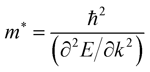 | (7) |
The band structure displays much larger dispersion around the CBM than the VBM, indicating low electron effective masses (∼0.39me in the CBM-Y direction) and high hole effective masses (∼7.34me in the VBM-V direction). Presuming the system is dopable, the low effective masses would result in greater electron mobility compared to hole mobility and therefore higher electrical conductivity for n-type doping. The low effective masses would, however, also lead to a reduced Seebeck coefficient, due to S being directly proportional to the density of states effective mass  (eqn (2)).
3.2 Electronic transport properties
Materials with valence bands dominated by O 2p states are not normally p-type dopable. The O 2p states are deep in energy with respect to the vacuum level, with large ionisation potentials, and the formation of localised oxygen hole polarons is therefore highly favoured in such materials.80 On the other hand, Sn(IV) compounds typically are n-type dopable.81–83 We therefore modelled the electrical properties of n-type doped α-Bi2Sn2O7, based on the HSE06 + SOC electronic structure, and up to the limit of 390 K at which the first phase transition takes place (Fig. 5).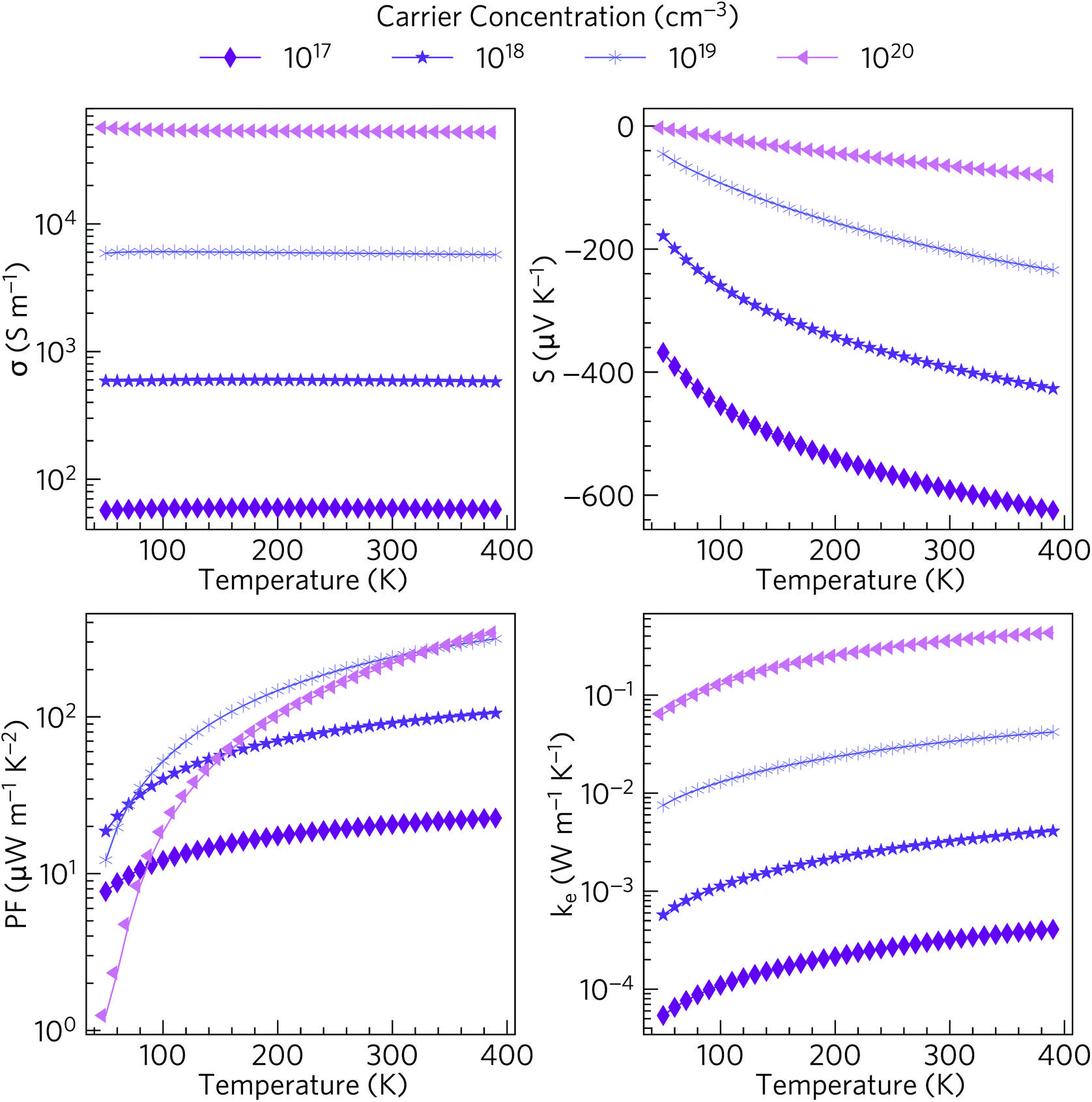 | ||
| Fig. 5 Predicted electronic transport properties of n-type doped α-Bi2Sn2O7 over the temperature range of 50–390 K: electrical conductivity σ, Seebeck coefficient S, power factor S2σ (PF) and electronic thermal conductivity κe. Values are calculated for carrier concentrations in the range of 1017 to 1020 cm−3. | ||
The electrical conductivities for carrier concentrations in the range of 1017 to 1020 cm−3 vary from around 6 × 101 to 6 × 10⁴ S m−1. The values obtained with the larger carrier concentrations are comparable to polycrystalline NaxCoO2−δ (σ = 5 × 10⁴ S m−1 at 300 K), which possesses one of the highest conductivities among current oxide thermoelectrics.13 The high σ is consistent with the dispersive character of the CBM and the resultant low electron effective mass and high carrier mobility.
For n-type transport the Seebeck coefficient is negative, and at room temperature ranges from around 64 to 591 µV K−1 at carrier concentrations of 1020 cm−3 and 1017 cm−3 respectively. The room-temperature Seebeck coefficient of 203 µV K−1 predicted for a carrier concentration of 1019 cm−3 is comparable to dual-doped Zn0.96Al0.02Ga0.02O (S ∼ 176 µV K−1 at 300 K), which has the highest reported ZT of the known n-type bulk oxide thermoelectrics.84
The combination of moderate electrical conductivity and high Seebeck coefficient results in power factors S2σ ranging from 8–343 µW m−1 K−2 at low temperatures/carrier concentrations and high temperatures/carrier concentrations respectively. Though the room temperature power factor of ∼220–240 µW m−1 K−2 at high carrier concentrations is lower than that of NaxCoO2 (2380 µW m−1 K−2 for single crystals and 500 µW m−1 K−2 for polycrystalline samples),13 they are comparable to the room temperature PFs of most other oxide thermoelectrics including p-type Ca3Co4O9 (∼150 µW m−1 K−2).85
The electronic thermal conductivities κe range from 5.4 × 10⁻⁵ at low temperature and low carrier concentration to 4.3 × 10⁻¹ W m−1 K−1 at high temperature and high carrier concentration. For moderate carrier concentrations the electrons thus make a small contribution to the thermal conductivity, and heat transport through the lattice is likely to dominate the total thermal conductivity, as is typical in semiconductors.
3.3 Phonon dispersion and density of states
Fig. 6 shows the simulated phonon dispersion of α-Bi2Sn2O7 together with the atom-projected phonon density of states (pDoS). The primitive cell contains 44 atoms, resulting in 3na = 132 phonon bands at each wave-vector (q-point) and introducing a large amount of fine structure into the dispersion and DoS. The dispersion shows no imaginary frequencies, confirming that the low-temperature α polymorph of Bi2Sn2O7 is dynamically stable.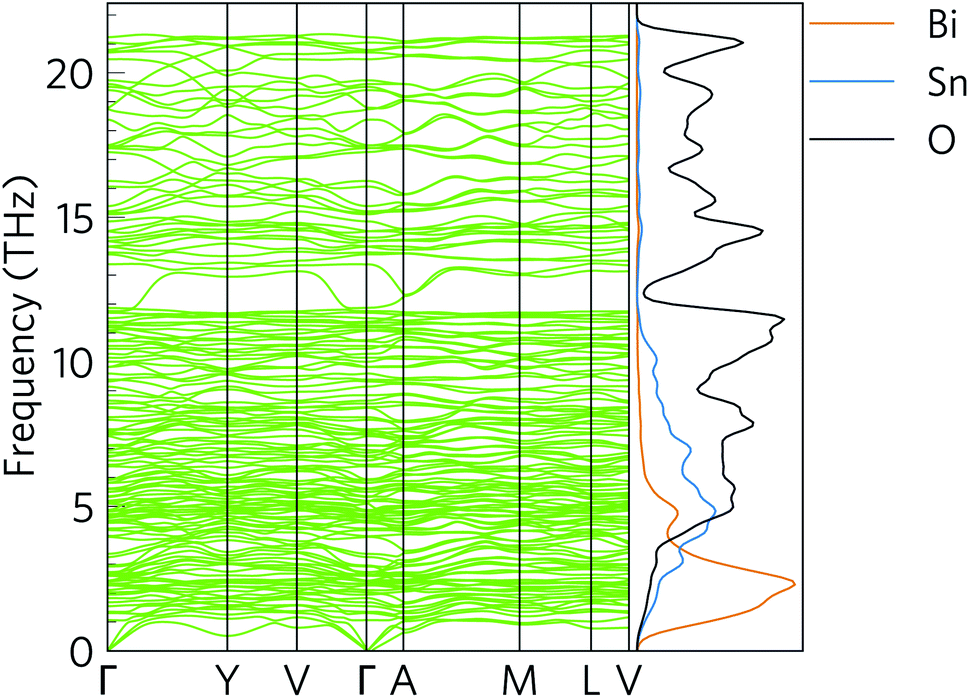 | ||
| Fig. 6 Simulated phonon dispersion and atom-projected density of states (pDoS) of α-Bi2Sn2O7. Projections of the DoS onto Bi, Sn and O atoms are shown in orange, blue and black respectively. | ||
The phonon spectrum spans a range of ∼21.2 THz. As expected from the inverse relationship between the reduced mass and vibrational frequency, the pDoS shows that low-frequency phonon modes up to ∼4 THz are primarily Bi vibrations with small contributions from Sn and O atoms. The intermediate 4–10 THz range is composed primarily of Sn/O vibrations, while the high frequency modes above 10 THz are predominantly O vibrations.
The relatively flat dispersion implies small group velocities νg = dω/dq, indicative of a low intrinsic lattice thermal conductivity κl. The low-frequency acoustic modes likely make larger contributions to κl than the optic modes due both to their broader dispersion/larger group velocity and their larger occupation number, which is given by the Bose–Einstein distribution:
 | (8) |
3.4 Lattice thermal conductivity
Fig. 7 shows the temperature dependence of the isotropically-averaged lattice thermal conductivity κiso together with the thermal conductivity along the three principal directions κxx, κyy and κzz. We calculate a room-temperature average κl of 0.401 W m−1 K−1, averaged over principal values of κxx = 0.398, κyy = 0.461 and κzz = 0.344 W m−1 K−1. This is the lowest ever calculated or measured for an oxide thermoelectric material near room temperature, and is lower than both SnSe (0.64/1.28 W m−1 K−1 (ref. 48 and 86)) and the industry-standard PbTe (1.9–2.2 W m−1 K−1 (ref. 87–89)). The κl values along the three lattice vectors differ only slightly, which is to be expected given that the low-temperature α phase of Bi2Sn2O7 remains structurally similar to the high-temperature cubic phase.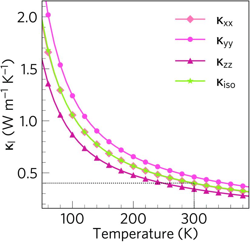 | ||
Fig. 7 Lattice thermal conductivity of α-Bi2Sn2O7 as a function of temperature calculated within the single-mode relaxation-time approximation and excluding isotope effects. The plot compares the principal xx (diamonds), yy (circles) and zz (triangles) components of the thermal-conductivity tensor with the diagonal average  (green stars). The dotted black line marks the room temperature (300 K) average κl of 0.401 W m−1 K−1). (green stars). The dotted black line marks the room temperature (300 K) average κl of 0.401 W m−1 K−1). | ||
Our calculated κl value is likely to be an upper limit, as the RTA only accounts for scattering via three-phonon processes and does not account for the effect of e.g. structural defects and boundary scattering. The measured κl would likely be further lowered by additional scattering from vacancies, substitutions and/or grain boundaries, if the sample is polycrystalline.
3.5 Modal contributions to the lattice thermal conductivity
To gain insight into the origin of the low room-temperature intrinsic κl of α-Bi2Sn2O7, we examined the modal thermal conductivities κλ, the group velocities norms |νλ|, the phonon lifetimes τλ and the phonon mean free paths Λλ as a function of frequency at 300 K (Fig. 8).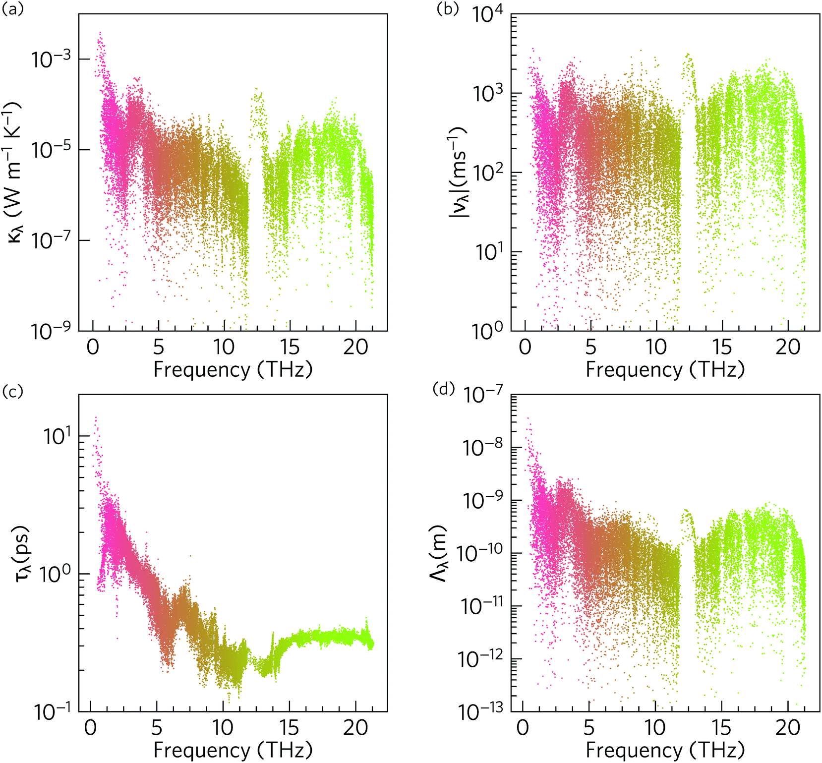 | ||
| Fig. 8 Analysis of the modal contributions to the 300 K lattice thermal conductivity of α-Bi2Sn2O7 defined in eqn (5): (a) isotropic modal thermal conductivities κλ, (b) group velocity norms |νλ|, (c) lifetimes τλ, and (d) mean free paths Λλ. The data points are coloured by band index. Note that a logarithmic scale is used for the y axis. | ||
The modes with the largest κλ are those with high group velocities and long lifetimes, and hence long mean free paths. As shown in Fig. 8(a) the acoustic modes make the largest contribution to κl at 300 K, followed by an order of magnitude smaller contribution from optic modes in the range of 3–5 THz, and then a smaller contribution again from the remainder of the phonon spectrum, with a slight enhancement around 18–19 THz.
Due to the tensor product in eqn (5), the κλ are proportional to ν2. As shown in Fig. 8(b), for the bulk of the modes the |νλ| fall within a range if 101 to 103 ms−1 and are relatively low due to the heavy atoms in the structure. The group velocities are largest around 1, 3 and 13 THz, which coincide with the peaks in the κλ spectrum. Inspection of the phonon dispersions in Fig. 6 shows regions around 0–1 and 12–13 THz where the modes have large dispersions, whereas over the remainder of the frequency spectrum the bands are relatively flat and indicative of smaller group velocities. The group velocities are comparable to the hybrid perovskite (CH3NH3)PbI3 (MAPbI3), for which an ultralow lattice thermal conductivity of 0.086 W m−1 K−1 has been calculated.90
The phonon lifetimes in Fig. 8(c) are those obtained by considering three-phonon scattering processes and, as noted above, are likely to be an upper limit due to the neglect of phenomena including higher-order phonon interactions, electron–phonon scattering, and defect and grain-boundary scattering. Across the phonon spectrum the lifetimes are <10 ps and are similar to those in highly-anharmonic compounds such as MAPbI3.91 The lifetimes of the acoustic modes are an order of magnitude longer than the optic modes. Since the κλ are linearly proportional to τλ, these longer lifetimes are an important factor in the large contribution of the acoustic modes to the overall κl.
The combination of short phonon lifetimes and small group velocities result in phonon mean free paths (Λλ) on the order of nanometers (Fig. 8(d)), with the majority being <10 nm. Whereas the spread in the mode group velocities is similar across the phonon spectrum, the strong frequency dependence of the phonon lifetimes results in the mean free paths of the acoustic modes being an order of magnitude longer than those of the optic modes. As expected from eqn (5) there is a strong correlation between Λλ and the modal κλ (Fig. S5†). However, the large number of atoms in the unit cell, and consequent small ratio of acoustic to optic modes, means the optic modes nonetheless make a substantial contribution to the overall κl.
This is clearly evident in the cumulative 300 K lattice thermal conductivity as a function of frequency (Fig. 9), which shows that modes from across the entire phonon spectrum, i.e. acoustic as well as low- and high-frequency optic modes, contribute to the heat transport. From the phonon dispersion, the acoustic modes span a range of ∼0 to 1.3 THz, and these modes contribute around 34% to the total κl. A further ∼41% of the total κl (i.e. 75% in total) is due to low-frequency optic modes up to 5 THz, and thus 75% of the κl arises from the 0–5 THz region of the phonon spectrum. Above 5 THz, the remaining 25% of the thermal conductivity is distributed almost evenly up to 21 THz. This differs markedly from SnSe92 and other conventional semiconductors such as GaAs and CdTe,90 where the majority of the heat is carried by the acoustic modes and is a consequence of the suppressed acoustic-mode transport, due to the low group velocities and short lifetimes, and the high proportion of optic modes compared to acoustic modes. (Of the 3na bands at each phonon wave-vector, 3 are acoustic modes and 3na − 3 are optic modes.) This highlights how materials with complex structures can be conducive to obtaining a low lattice thermal conductivity and improving the thermoelectric performance.2 A significant contribution of optic modes to the heat transport is also seen in MAPbI3, where transport through the acoustic modes is similarly suppressed.90
 | ||
| Fig. 9 Cumulative % lattice thermal conductivity of α-Bi2Sn2O7 at 300 K as a function of frequency (green) overlaid against the phonon density of states projected onto the Bi (orange), Sn (blue) and O (black) atoms. | ||
3.6 Microscopic origin of short phonon mode lifetimes
As noted above the phonon lifetimes are obtained from the phonon linewidths Γλ as: | (9) |
 | (10) |
The 2D histogram in Fig. 10 shows the pairwise contributions of modes with frequency νλ′ and νλ″ to the linewidths of the modes from 0–5 THz identified in the previous section as being responsible for the majority of the heat transport in α-Bi2Sn2O7.91 This analysis shows that strong interactions with acoustic and low-frequency optic modes are primarily responsible for the broadening of these modes. Scattering with modes up to 13 THz also makes a significant contribution, while scattering processes involving the high-frequency optical modes have a relatively small impact.
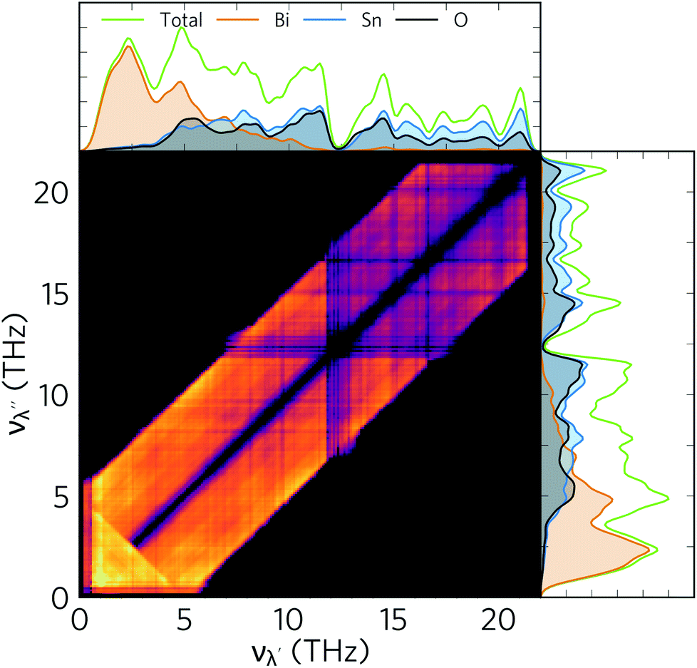 | ||
| Fig. 10 2D histogram showing the pairwise contribution of modes λ′ and λ″, with frequencies νλ′ and νλ″, to the linewidth of the modes with ν = 0–5 THz in α-Bi2Sn2O7. The colour scale is logarithmic and runs from black (zero contribution) to yellow (large contribution). The phonon density of states (green), and its projections onto Bi (orange), Sn (blue), and O atoms (black) is shown against both axes for comparison. | ||
The large dispersion of acoustic modes typically limits decay channels at low frequencies so that collisions are the dominant mechanism for acoustic-mode scattering. The large number of low-lying optic modes in α-Bi2Sn2O7 would be significantly populated at room temperature and provide means of “absorbing” acoustic phonons. A similar histogram analysis of the entire frequency spectrum (Fig. S7†) shows that the other modes in α-Bi2Sn2O7 are also heavily broadened by scattering with modes in the low-frequency part of the spectrum. This region of the spectrum is dominated by Bi3+ vibrations, indicating that the heavy cations play a major role in the short mode lifetimes in α-Bi2Sn2O7. The Bi atoms thus serve a dual function in suppressing the thermal transport in α-Bi2Sn2O7: the large mass and weak Bi–O chemical bonding lowers the group velocities, while the resultant low-frequency vibrations enable a large number of decay pathways.
The requirement to conserve energy and (crystal) momentum in three-phonon scattering processes means that the shape of the phonon spectrum plays an important role in defining the number of available scattering pathways. The high density of low-frequency modes in the α-Bi2Sn2O7 phonon spectrum would naturally provide a large number of energy-conserving scattering channels. In addition to this, by analogy with SnSe, the presence of the active lone pairs of electrons around Bi may also facilitate stronger phonon–phonon interactions.86 To investigate the relative importance of these two contributions, we followed the analysis proposed in ref. 67. The phonon linewidths Γλ can be approximated by the product of an averaged three-phonon interaction strength Pλ and a two-phonon joint density of states Nλ (JDoS) which counts the number of energy- and momentum-conserving scattering channels available for a reference mode with frequency ωλ:
 | (11) |
 | (12) |
 | (13) |
 | (14) |
![[N with combining macron]](https://www.rsc.org/images/entities/i_char_004e_0304.gif) 2(ωλ) which are averaged over the phonon wavevector q.
2(ωλ) which are averaged over the phonon wavevector q.
Fig. 11 compares the spectrum of phonon linewidths of α-Bi2Sn2O7 at 300 K to this averaged two-phonon density of states and the spectrum of phonon interaction strengths. The Γλ show an inverse relationship to the lifetimes in Fig. 8, i.e. are narrow for the low-frequency modes and become broader at higher frequencies. Comparison of the Γλ with the JDoS 2(ωλ) shows that the linewidths closely track the JDoS. This is particularly evident from 0 to 7.5 THz where the steep rise in the linewidth mirrors the sharp increase in the number of available scattering channels. The JDoS shows that Type 1 scattering events (collisions) are dominant at low frequency while Type 2 events (decay) become active around from around 5 THz and dominate at higher frequencies. Since spontaneous decay requires two modes with suitable energy and momentum to decay into, this pathway is only feasible for higher-energy modes. This confirms the main inference drawn from the 2D histogram analysis – that the low-frequency modes are predominantly scattered by interactions with other acoustic modes and low-lying optic modes.
 | ||
| Fig. 11 Analysis of the phonon linewidths in α-Bi2Sn2O7 using eqn (11–14). (a) Mode linewidths Γλ as a function of frequency. (b) Two-phonon density of states 2(ωλ) showing the density of energy- and momentum-conserving three-phonon scattering channels as a function of frequency. Contributions from collisions (Type 1 events, 2(1)) and decay events (Type 2 events, 2(2)) are shown separately. (c) Averaged three-phonon interaction strength Pλ. The data points in (a) and (c) are coloured by band index. Note that the y-axis in (b) is on a linear scale while the axes in (a) and (c) are on a logarithmic scale. | ||
The Pλ show a marked dip between 0–5 THz, which is reflected in the linewidths but counteracted by the steep increase in the JDoS over this frequency range. Across the entire spectrum, the linewidths are broadest at intermediate frequencies, which can be attributed to the large number of collision and decay channels available in this region. The averaged interaction strengths are stronger and show comparatively little variation at higher frequencies, which further explains the shorter lifetimes of these modes. Comparison with MAPbI3 shows that the phonon–phonon interaction strengths are fairly weak and are more similar in magnitude to GaAs and CdTe.90 We can therefore infer that the dominant factor in the short lifetimes and limited thermal transport in α-Bi2Sn2O7 is the high density of scattering channels. This is a consequence of the shape of the spread of frequencies in the dispersion and DoS rather than strong interactions between modes. This can be attributed to the asymmetric bonding environment caused by the lone pair activity on the Bi cations inducing structural distortions from the high-temperature cubic phase.
3.7 Nanostructuring
The lattice thermal conductivity in thermoelectrics can be further reduced by employing a range of hierarchical approaches, of which nanostructuring is among the most popular.93,94 Analysis of modal contributions to lattice thermal conductivity shows that it is the Bi-dominant low-frequency modes that make the greatest contributions to κl due to their longer mean free paths. Therefore, nanostructuring to suppress such modes is an obvious route to further reducing the thermal conductivity. One route to achieve this is to disperse nanoparticles into the material. Dispersal of ErAs nanoparticles into In0.53Ga0.47As alloys was used to successfully reduce the κl,95 while nanostructuring AgPb18SbTe20 to 20–30 nm drastically increased the thermoelectric figure of merit from 0.5 to 2.2.96,97 However, the mean free paths in α-Bi2Sn2O7 are close to typical grain sizes, with the majority being less than 10 nm (see Fig. 8), which means nanostructuring is unlikely to be quite so fruitful here. However, nanostructuring down to 5 nm has been demonstrated for Ag1−xSb1+xTe2+x (x = 0, 0.1 and 0.2), resulting in a very low κl of only 0.7 W m−1 K−1.98We therefore modelled the effect of nanostructuring at two different length scales, viz. 10 nm and 5 nm, using a simple boundary scattering model which limits the contributions to κl from modes with mean free paths greater than the cutoff. As expected, imposing boundary scattering limits comparable to the acoustic mode mean free paths further reduces κl, as shown in Fig. 12. The room temperature isotropically averaged κl is reduced from 0.401 to 0.314 and 0.277 W m−1 K−1 for grain sizes of 10 and 5 nm, respectively, indicating that if nanostructuring is possible down to these length scales it could significantly reduce κl. Nanostructuring is also likely to decrease the electrical conductivity σ but would also therefore decrease κe which, along with the appreciable reduction in κl, may lead to an overall increase the ZT.
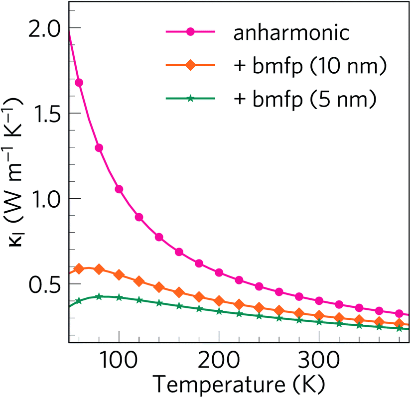 | ||
| Fig. 12 Isotropically averaged lattice thermal conductivity κl of α-Bi2Sn2O7 as a function of temperature with a boundary scattering model used to mimic the effect of nanostructuring at different length scales. The plot compares κl obtained without boundary scattering (pink circles) to values obtained with maximum phonon mean free paths of 10 nm (orange diamonds) and 5 nm (teal stars). | ||
3.8 Maximum ZT and comparison with other oxide and low temperature thermoelectrics
Fig. 13 shows the predicted variation of the figure of merit ZT of n-type doped α-Bi2Sn2O7 as a function of carrier concentration and temperature. The ZT value at each temperature and concentration is obtained by combining the predicted electrical properties and lattice thermal conductivity obtained in the previous sections. The maximum room temperature (300 K) ZT, where κl = 0.401 W m−1 K−1, is predicted to be 0.180 and occurs at an electron carrier concentration of 1.54 × 1019 cm−3. The maximum ZT of 0.359 is predicted to occur at 385 K (κl = 0.322 W m−1 K−1) with a carrier concentration of 1.73 × 1019 cm−3, and is the highest low temperature ZT predicted for an oxide thermoelectric at the time of writing.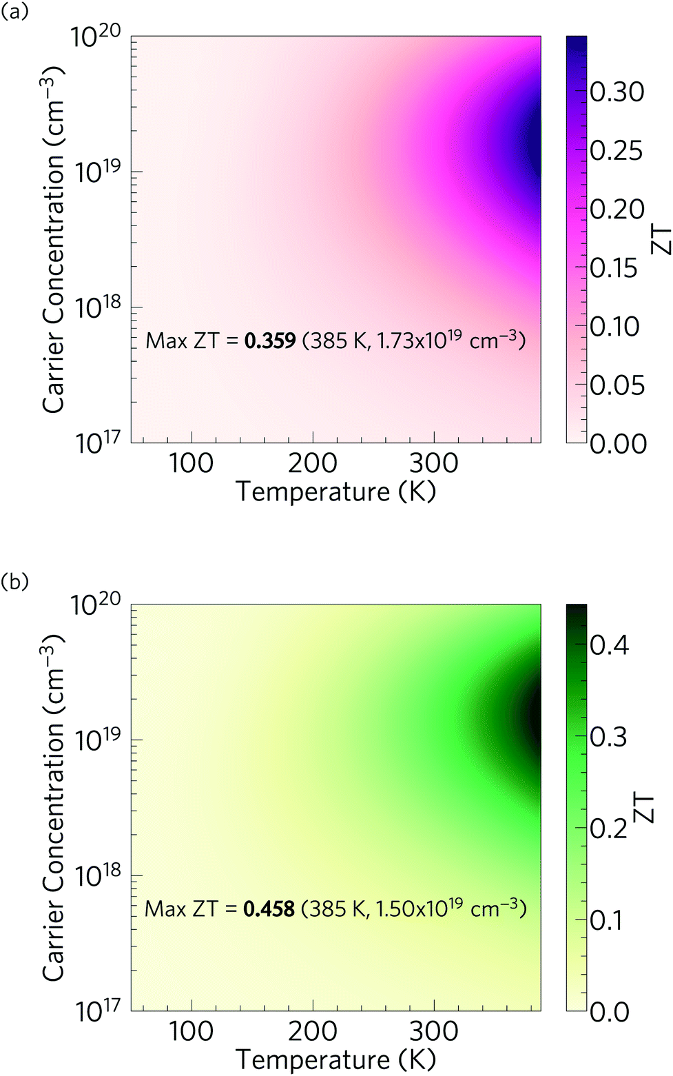 | ||
| Fig. 13 Predicted thermoelectric figure of merit ZT of n-type doped α-Bi2Sn2O7 as a function of temperature and carrier concentration. Plot (a) shows the predictions obtained based on the thermal conductivity calculated for the bulk material, while (b) shows the improved performance obtained by nanostructuring to 5 nm. | ||
With the reduction in κl obtained by nanostructuring to 5 nm (Fig. 12), and under the assumption of a minimal effect on the electronic transport, we predict a room-temperature ZT of 0.246 (κl = 0.277 W m−1 K−1; carrier concentration of 1.40 × 1019 cm−3), and a maximum ZT of 0.458 at 385 K (κl = 0.237 W m−1 K−1, carrier concentration of 1.50 × 1019 cm−3) (Fig. 13). Although nanostructuring to such a small size is challenging, it would substantially improve its TE performance, and given the very short phonon mean free paths predicted by the thermal-conductivity calculations, nanostructuring at larger length scales would have comparatively little effect.
Since the structure undergoes a phase transition above 390 K, it may not be suitable for high-temperature industrial applications, but could be used to improve the efficiency of consumer devices that generate heat at or below 100 °C. Such applications might include for example recovering heat from exhaust gases in domestic boilers, recovering wasted energy from microprocessors, and battery conditioning in electric vehicles. The possibility of using a thermoelectric generator to improve the efficiency of domestic boilers is a particularly topical application given the large contribution of gas central heating to carbon emissions and the infrastructure challenges of replacing this with cleaner alternatives such as hydrogen.99,100
A comparison of α-Bi2Sn2O7 to other oxide thermoelectrics shows that it does not possess an exceptionally high or low power factor, but that its high predicted room temperature ZT results from its ultra-low intrinsic κl. p-type NaCo2O4 is one of the earliest reported oxide thermoelectrics,12 and single crystals of NaxCoO2−δ have high power factors comparable to the industry standard Bi2Te3. However, this material has a room temperature ZT of only 0.036 due to its high κl of ∼16.5 W m−1 K−1,13 which is around 40 × higher than our predicted 0.4 W m−1 K−1 for α-Bi2Sn2O7. Similarly, p-type Ca3Co4O9 only attains a ZT of around 0.07 at 300 K (∼0.83 at 973 K),14 again due to a large κl of around 3 W m−1 K−1. Finally, Bi2Sr2Co2Oy, which has a layered structure similar to NaCo2O4 and Ca3Co4O9, still has thermal conductivities ranging from 1.7 to 1.9 W m−1 K−1, up to 5 × larger than Bi2Sn2O7, and as a result gives a low-temperature ZT of only 0.06 to 0.09, only rising to ∼1.1 at a very high temperature of 973 K.15 The room-temperature polymorph of Bi2Sn2O7 is thus predicted to perform significantly better than some of the best known p-type oxide thermoelectric materials at low temperature.
Comparison with n-type oxide semiconductors further highlights the potential thermoelectric performance of α-Bi2Sn2O7. La- and Nb-doped single crystals of the cubic perovskite SrTiO3 show very high electrical conductivity and power factors,16 but both have large room-temperature thermal conductivities, in the range of 9 to 12 W m−1 K−1, resulting in a maximum 300 K ZT of only ∼0.03, which is 6 × smaller than that predicted for α-Bi2Sn2O7. The n-type oxide semiconductor CaMnO3 has a large κl of 2–4 W m−1 K−1 at room temperature, resulting in ZT < 0.05 even after substitution.17–19 Dual-doped ZnO with Al and Ga has the highest reported ZT among the n-type oxides, with a power factor comparable to conventional thermoelectrics such as Bi2Te3, PbTe and Si–Ge.84 Its room-temperature thermal conductivity is, however, almost 30 times larger than Bi2Sn2O7 (∼13 W m−1 K−1 for Zn0.96Al0.02Ga0.02O), and it again only reaches a low ZT of only 0.14 at room temperature.
At present, the industry-standard materials for low-temperature power generation are the Bi2Te3 alloys. Conventional Bi2Te3-based materials attain a ZT of around 1 at room temperature,101 and further enhancements above unity have been achieved by tuning the composition, either by introducing ternary phases or by doping, and by optimising the fabrication methods.102–104 The lattice thermal conductivities range between 0.2–0.7 W m−1 K−1 for compositionally-tuned and nanostructured samples,102–106 but it is mainly the outstanding power factors that are responsible for its higher ZT in comparison to α-Bi2Sn2O7. α-Bi2Sn2O7 is, however, composed of earth-abundant and cheap constituent elements, in contrast to the rare and expensive tellurium required to form Bi2Te3.
CsBi4Te6 has also shown promise as a room-temperature thermoelectric, with very high power factors above 5000 µW m−1 K−2 in p-type doped samples producing high ZT values of around 0.82 at 225 K. However, this material has been predicted to have a κl of 0.87 W m−1 K−1,107 almost twice that of α-Bi2Sn2O7, and again requires rare and expensive Te.
Recently, Mao et al. have demonstrated the potential of Mg3Bi2-based alloys, which, unlike Bi2Te3 and CsBi4Te6, consist of earth-abundant elements.108 Doping with small amounts of Te increases the power factor to 2000 µ W m−1 K−2, resulting in a ZT of 0.3 at 350 K, which is lower than the maximum ZT predicted for α-Bi2Sn2O7. The low ZT was attributed to high κl of between 2–3 W m−1 K−1 at low temperatures, which can be reduced by partial substitution of Bi with Sb, leading to a maximum ZT of 0.9 at 350 K for n-type Mg3.2Bi1.298Sb0.7Te0.002. It should be noted that although the maximum ZT obtained for α-Bi2Sn2O7 is lower than the current best low-temperature thermoelectric materials, we have not investigated strategies such as alloying or band-structure engineering which may help to further improve the thermoelectric performance.
On the other hand, α-Bi2Sn2O7 stands out among other oxide thermoelectrics as having a very low room-temperature lattice thermal conductivity. The strong chemical bonding in most oxide materials leads to large group velocities and, at best, moderate κl values. The heavy metal cations in Bi2Sn2O7 naturally impart weaker bonding and lower group velocities. Furthermore, the structural distortion induced by the active lone pair spreads out the phonon frequencies and results in a complex structure and a dense phonon dispersion, and this, together with the low-frequency vibrations associated with the Bi cations, produces a high density of energy-conserving scattering channels and leads to very short phonon lifetimes. These unusual lattice dynamics lead to the highest room-temperature ZT predicted so far for an oxide material.
4 Conclusions
We have used state-of-the-art quantum chemistry techniques to predict the thermoelectric properties of the room-temperature α polymorph of the heavy metal oxide Bi2Sn2O7. Lattice-dynamics calculations suggest that α-Bi2Sn2O7 possesses an ultralow lattice thermal conductivity of 0.4 W m−1 K−1 at 300 K, the lowest ever predicted for an oxide at room temperature, due to a combination of low group velocities and extremely short phonon lifetimes. This low lattice thermal conductivity yields a room temperature n-type ZT of 0.18 and a maximum ZT of 0.36 at 385 K, which represent the highest low-temperature values yet predicted for an oxide thermoelectric. Despite having lower ZT than the industry-standard Bi2Te3, it offers the advantage of being composed of earth-abundant and cheap elements and therefore being suitable for widespread deployment. Our calculations suggest that its thermoelectric properties might be further improved by nanostructuring. A detailed analysis of the short phonon lifetimes shows that the structural distortions induced by the active lone pairs on the Bi cations produce a high density of phonon scattering pathways. This effect reinforces the naturally low group velocities arising from the weak chemical bonding associated with the heavy metals, and results in an ultra-low lattice thermal conductivity. The importance of its dopability for practical application as a thermoelectric material should not be underestimated. However, regardless of whether it can be doped or not this work provides a blueprint for improving the performance of oxide thermoelectrics by looking to complex multiternary systems with heavy cations, and thus paves the way for the guided discovery of other low-temperature oxide thermoelectrics.Conflicts of interest
The authors declare no competing financial interests.Acknowledgements
Via our membership of the UKs HEC Materials Chemistry Consortium, which is funded by EPSRC (EP/L000202, EP/R029431), this work used the ARCHER UK National Supercomputing Service (http://www.archer.ac.uk). We are also grateful to the UK Materials and Molecular Modelling Hub for computational resources, which is partially funded by EPSRC (EP/P020194/1), and to UCL for access to the Legion (Legion@UCL), Myriad (Myriad@UCL) and Grace (Grace@UCL) supercomputers. WR is grateful to University College London for awarding the PhD scholarship. JMS is grateful to the University of Manchester for the award of a Presidential Fellowship.Notes and references
- D. T. Morelli, Encyclopedia of Applied Physics, 1997, 21, 339 Search PubMed.
- F. J. Disalvo, Science, 1999, 285, 703 CrossRef PubMed.
- T. M. Tritt, Annu. Rev. Mater. Res., 2011, 41, 433 CrossRef CAS.
- R. Franz and G. Wiedemann, Ann. Phys., 1853, 165, 497 CrossRef.
- L.-D. Zhao, C. Chang, G. Tan and M. G. Kanatzidis, Energy Environ. Sci., 2016, 9, 3044 RSC.
- Y. Pei, C. Chang, Z. Wang, M. Yin, M. Wu, G. Tan, H. Wu, Y. Chen, L. Zheng, S. Gong, T. Zhu, X. Zhao, L. Huang, J. He, M. G. Kanatzidis and L. D. Zhao, J. Am. Chem. Soc., 2016, 138, 16364 CrossRef CAS PubMed.
- T. J. Slade, J. A. Grovogui, S. Hao, T. P. Bailey, R. Ma, X. Hua, A. Gue, C. Uher, C. Wolverton, V. P. Dravid and M. G. Kanatzidis, J. Am. Chem. Soc., 2018, 140, 7021 CrossRef CAS PubMed.
- J. Li, Y. Zhou, S. Hao, T. Zhang, C. Wolverton, J. Zhao and L.-D. Zhao, Inorg. Chem., 2019, 58, 1339 CrossRef PubMed.
- H. Xie, X. Su, X. Zhang, S. Hao, T. P. Bailey, C. C. Stoumpos, A. P. Douvalis, X. Hu, C. Wolverton, V. P. Dravid, C. Uher, X. Tang and M. G. Kanatzidis, J. Am. Chem. Soc., 2019, 141, 10905 CrossRef PubMed.
- S. Pan, C. Wang, Q. Zhang, B. Yang, Y. Cao, L. Liu, Y. Jiang, L. You, K. Guo, J. Zhang, J. Yang, J. Luo and W. Zhang, ACS Appl. Energy Mater., 2019, 2, 8956 CrossRef.
- Y. Feng, X. Jiang, E. Ghafari, B. Kucukgok, C. Zhang, I. Ferguson and N. Lu, Adv. Compos. Hybrid Mater., 2018, 1, 114 CrossRef.
- I. Terasaki, Y. Sasago and K. Uchinokura, Phys. Rev. B: Condens. Matter Mater. Phys., 1997, 56, R12685 CrossRef.
- K. Fujita, T. Mochida and K. Nakamura, Jpn. J. Appl. Phys., 2001, 40, 4644 CrossRef.
- M. Shikano and R. Funahashi, Appl. Phys. Lett., 2003, 82, 1851 CrossRef.
- R. Funahashi and M. Shikano, Appl. Phys. Lett., 2002, 81, 1459 CrossRef.
- S. Ohta, T. Nomura, H. Ohta and K. Koumoto, J. Appl. Phys., 2005, 97, 34106 CrossRef.
- M. Ohtaki, H. Koga, T. Tokunaga, K. Eguchi and H. Arai, J. Solid State Chem., 1995, 120, 105 CrossRef.
- D. Flahaut, T. Mihara, R. Funahashi, N. Nabeshima, K. Lee, H. Ohta and K. Koumoto, J. Appl. Phys., 2006, 100, 084911 CrossRef.
- G. Xu, R. Funahashi, Q. Pu, B. Liu, R. Tao, G. Wang and Z. Ding, Solid State Ionics, 2004, 171, 147 CrossRef.
- J. W. Fergus, J. Eur. Ceram. Soc., 2012, 32, 525 CrossRef.
- K. B. Spooner, A. M. Ganose and D. O. Scanlon, J. Mater. Chem. A, 2020, 8, 11948 RSC.
- H. Muta, K. Kurosaki and S. Yamanaka, J. Alloys Compd., 2004, 368, 22 CrossRef.
- L. M. Daniels, S. N. Savvin, M. J. Pitcher, M. S. Dyer, J. B. Claridge, S. Ling, B. Slater, F. Corà, J. Alaria and M. J. Rosseinsky, Energy Environ. Sci., 2017, 10, 1917 RSC.
- A. Goyal, P. Gorai, E. S. Toberer and V. Stevanović, npj Comput. Mater., 2017, 3, 42 CrossRef.
- R. D. Shannon, J. D. Berlein, J. L. Gillson, G. A. Jon and A. W. Sleight, J. Phys. Chem. Solids, 1980, 41, 117 CrossRef.
- J. W. Lewis, J. L. Payne, I. R. Evans, H. T. Stokes, B. J. Campbell and J. S. O. Evans, J. Am. Chem. Soc., 2016, 138, 8031 CrossRef PubMed.
- I. R. Evans, J. A. K. Howard and J. S. O. Evans, J. Mater. Chem., 2003, 13, 2098 RSC.
- W. Rahim, J. M. Skelton, C. N. Savory, I. R. Evans, J. S. O. Evans, A. Walsh and D. O. Scanlon, Chem. Sci., 2020 10.1039/D0SC02995E.
- K. Momma and F. Izumi, J. Appl. Crystallogr., 2011, 44, 1272 CrossRef.
- D. P. Shoemaker, R. Seshadri, M. Tachibana and A. L. Hector, Phys. Rev. B: Condens. Matter Mater. Phys., 2011, 84, 064117 CrossRef.
- A. Walsh and G. W. Watson, Chem. Mater., 2007, 19, 5158 CrossRef.
- S. C. Dixon, S. Sathasivam, B. A. D. Williamson, D. O. Scanlon, C. J. Carmalt and I. P. Parkin, J. Mater. Chem. C, 2017, 5, 7585 RSC.
- M. J. Powell, B. A. D. Williamson, S. Y. Baek, J. Manzi, D. B. Potter, D. O. Scanlon and C. J. Carmalt, Chem. Sci., 2018, 9, 7968 RSC.
- S. D. Ponja, B. A. D. Williamson, S. Sathasivam, D. O. Scanlon, I. P. Parkin and C. J. Carmalt, J. Mater. Chem. C, 2018, 6, 7257 RSC.
- J. E. N. Swallow, B. A. D. Williamson, T. J. Whittles, M. Birkett, T. J. Featherstone, N. Peng, A. Abbott, M. Farnworth, K. J. Cheetham, P. Warren, D. O. Scanlon, V. R. Dhanak and T. D. Veal, Adv. Funct. Mater., 2018, 28, 1701900 CrossRef.
- B. A. D. Williamson, T. J. Featherstone, S. S. Sathasivam, J. E. N. Swallow, H. Shiel, L. A. H. Jones, M. J. Smiles, A. Regoutz, T.-L. Lee, X. Xia, C. Blackman, P. K. Thakur, C. J. Carmalt, I. P. Parkin, T. D. Veal and D. O. Scanlon, Chem. Mater., 2020, 32, 1964 CrossRef PubMed.
- J. E. N. Swallow, B. A. D. Williamson, S. Sathasivam, M. Birkett, T. J. Featherstone, P. A. E. Murgatroyd, H. J. Edwards, Z. W. Lebens-Higgins, D. A. Duncan, M. Farnworth, P. Warren, N. Peng, T. L. Lee, L. F. Piper, A. Regoutz, C. J. Carmalt, I. P. Parkin, V. R. Dhanak, D. O. Scanlon and T. D. Veal, Mater. Horiz., 2020, 7, 236 RSC.
- M. Burbano, D. O. Scanlon and G. W. Watson, J. Am. Chem. Soc., 2011, 133, 15065 CrossRef PubMed.
- Z. Lebens-Higgins, D. O. Scanlon, H. Paik, S. Sallis, Y. Nie, M. Uchida, N. F. Quackenbush, M. J. Wahila, G. E. Sterbinsky, D. A. Arena, J. C. Woicik, D. G. Schlom and L. F. J. Piper, Phys. Rev. Lett., 2016, 116, 027602 CrossRef PubMed.
- W. Kohn and L. J. Sham, Phys. Rev., 1965, 140, A1133 CrossRef.
- G. Kresse and J. Hafner, Phys. Rev. B: Condens. Matter Mater. Phys., 1993, 47, 558 CrossRef PubMed.
- G. Kresse and J. Hafner, Phys. Rev. B: Condens. Matter Mater. Phys., 1994, 49, 14251 CrossRef CAS.
- G. Kresse and J. Furthmuller, Comput. Mater. Sci., 1996, 6, 15 CrossRef CAS.
- G. Kresse and J. Furthmüller, Phys. Rev. B: Condens. Matter Mater. Phys., 1996, 54, 11169 CrossRef CAS PubMed.
- J. P. Perdew, A. Ruzsinszky, G. I. Csonka, O. A. Vydrov, G. E. Scuseria, L. A. Constantin, X. Zhou and K. Burke, Phys. Rev. Lett., 2007, 100, 136406 CrossRef PubMed.
- J. P. Perdew, K. Burke and M. Ernzerhof, Phys. Rev. Lett., 1996, 77, 3866 CrossRef PubMed.
- J. M. Skelton, D. Tiana, S. C. Parker, A. Togo, I. Tanaka and A. Walsh, J. Chem. Phys., 2015, 143, 64710 CrossRef PubMed.
- J. M. Skelton, L. A. Burton, S. C. Parker, A. Walsh, C.-E. Kim, A. Soon, J. Buckeridge, A. A. Sokol, C. R. A. Catlow, A. Togo and I. Tanaka, Phys. Rev. Lett., 2016, 117, 075502 CrossRef PubMed.
- A. M. Ganose, M. Cuff, K. T. Butler, A. Walsh and D. O. Scanlon, Chem. Mater., 2016, 28, 1980 CrossRef PubMed.
- A. M. Ganose, K. T. Butler, A. Walsh and D. O. Scanlon, J. Mater. Chem. A, 2016, 4, 2060 RSC.
- M. A. Tumelero, L. C. Benetti, E. Isoppo, R. Faccio, G. Zangari and A. A. Pasa, J. Phys. Chem. C, 2016, 120, 11797 CrossRef CAS.
- P. E. Blöchl, Phys. Rev. B: Condens. Matter Mater. Phys., 1994, 50, 17953 CrossRef PubMed.
- P. Pulay, Mol. Phys., 1969, 17, 197 CrossRef CAS.
- A. V. Krukau, O. A. Vydrov, A. F. Izmaylov and G. E. Scuseria, J. Chem. Phys., 2006, 125, 6158 CrossRef PubMed.
- C. N. Savory, A. M. Ganose, W. Travis, R. S. Atri, R. G. Palgrave and D. O. Scanlon, J. Mater. Chem., 2016, 4, 12648 RSC.
- A. M. Ganose, C. N. Savory and D. O. Scanlon, J. Mater. Chem. A, 2017, 5, 7845 RSC.
- D. Hobbs, G. Kresse and J. Hafner, Phys. Rev. B: Condens. Matter Mater. Phys., 2000, 62, 11556 CrossRef CAS.
- A. M. Ganose, A. J. Jackson and D. O. Scanlon, J. Open Source Softw., 2018, 3, 717 CrossRef.
- J. R. Chelikowsky and S. G. Louie, Quantum Theory of Real Materials, Kluwer, Boston, 1996 Search PubMed.
- J. M. Ziman, Electrons and Phonons: The Theory of Transport Phenomena in Solids, Oxford Univ. Press, 2001 Search PubMed.
- G. K. H. Madsen and D. J. Singh, Comput. Phys. Commun., 2006, 175, 67 CrossRef CAS.
- D. Wang, L. Tang, M. Long and Z. Shuai, J. Chem. Phys., 2009, 131, 224704 CrossRef PubMed.
- R. Chmielowski, D. Péré, C. Bera, I. Opahle, W. Xie, S. Jacob, F. Capet, P. Roussel, A. Weidenkaff, G. K. H. Madsen and G. Dennler, J. Appl. Phys., 2015, 117, 125103 CrossRef.
- H. Shi, D. Parker, M.-H. Du and D. J. Singh, Phys. Rev. Appl., 2015, 3, 014004 CrossRef.
- A. Togo, F. Oba and I. Tanaka, Phys. Rev. B: Condens. Matter Mater. Phys., 2008, 78, 134106 CrossRef.
- A. Togo and I. Tanaka, Scr. Mater., 2015, 108, 1 CrossRef CAS.
- A. Togo, L. Chaput and I. Tanaka, Phys. Rev. B: Condens. Matter Mater. Phys., 2015, 91, 094306 CrossRef.
- K. Parlinski, Z. Q. Li and Y. Kawazoe, Phys. Rev. Lett., 1997, 78, 4063 CrossRef CAS.
- G. Kresse, J. Furthmüller and J. Hafner, Europhys. Lett., 1995, 32, 729 CrossRef.
- A. H. Romero, M. Cardona, R. K. Kremer, R. Lauck, G. Siegle, J. Serrano and X. C. Gonze, Phys. Rev. B: Condens. Matter Mater. Phys., 2008, 78, 224302 CrossRef.
- A. H. Macdonald, S. H. Voskot and P. T. Coleridges, J. Phys. C: Solid State Phys., 1979, 12, 2991 CrossRef.
- P. E. Blochl, O. Jepsen and O. K. Andersen, Phys. Rev. B: Condens. Matter Mater. Phys., 1994, 49, 16223 CrossRef PubMed.
- T. Tadano, Y. Gohda and S. Tsuneyuki, J. Phys.: Condens. Matter, 2014, 26, 225402 CrossRef.
- A. Walsh, D. J. Payne, R. G. Egdell and G. W. Watson, Chem. Soc. Rev., 2011, 40, 4455 RSC.
- A. Walsh, G. W. Watson, D. J. Payne, G. Atkinson and R. G. Egdell, J. Mater. Chem., 2006, 16, 3452 RSC.
- A. J. Jackson, A. M. Ganose, A. Regoutz, R. G. Egdell and D. O. Scanlon, J. Open Source Softw., 2018, 3, 773 CrossRef.
- U. Gelius and K. Siegbahn, Faraday Discuss. Chem. Soc., 1972, 54, 257 RSC.
- J. J. Yeh and I. Lindau, At. Data Nucl. Data Tables, 1985, 32, 1 CrossRef CAS.
- B. Van Zeghbroeck, Principles of Semiconductor Devices, University of Colorado, Boulder CO, 2004 Search PubMed.
- D. O. Scanlon and G. W. Watson, J. Mater. Chem., 2012, 22, 25236 RSC.
- D. O. Scanlon, Phys. Rev. B: Condens. Matter Mater. Phys., 2013, 87, 161201 CrossRef.
- A. E. Maughan, A. M. Ganose, M. M. Bordelon, E. M. Miller, D. O. Scanlon and J. R. Neilson, J. Am. Chem. Soc., 2016, 138, 44 CrossRef.
- A. M. Ganose and D. O. Scanlon, J. Mater. Chem. C, 2016, 4, 1467 RSC.
- M. Ohtaki, K. Araki and K. Yamamoto, J. Electron. Mater., 2009, 38, 1234 CrossRef CAS.
- R. Tian, R. Donelson, C. D. Ling, P. E. R. Blanchard, T. Zhang, D. Chu, T. Teck Tan and S. Li, J. Phys. Chem. C, 2013, 117, 13382 CrossRef CAS.
- L.-D. Zhao, S.-H. Lo, Y. Zhang, H. Sun, G. Tan, C. Uher, C. Wolverton, V. P. Dravid and M. G. Kanatzidis, Nature, 2014, 508, 373 CrossRef CAS.
- A. A. El-Sharkawy, A. M. Abou Ei-Azm, M. I. Kenawy, A. S. Hillal and H. M. Abu-Basha, Int. J. Thermophys., 1983, 4, 261 CrossRef CAS.
- G. A. Akhmedova and D. S. Abdinov, Inorg. Mater., 2009, 45, 854 CrossRef CAS.
- J. M. Skelton, S. C. Parker, A. Togo, I. Tanaka and A. Walsh, Phys. Rev. B: Condens. Matter Mater. Phys., 2014, 89, 205203 CrossRef.
- L. D. Whalley, J. M. Skelton, J. M. Frost and A. Walsh, Phys. Rev. B, 2016, 94, 220301 CrossRef.
- A. Gold-Parker, P. M. Gehring, J. M. Skelton, I. C. Smith, D. Parshall, J. M. Frost, H. I. Karunadasa, A. Walsh and M. F. Toney, Proc. Natl. Acad. Sci. U. S. A., 2018, 115, 11905 CrossRef CAS PubMed.
- J. Carrete, N. Mingo and S. Curtarolo, Appl. Phys. Lett., 2014, 105, 101907 CrossRef.
- K. Biswas, J. He, I. D. Blum, C.-I. Wu, T. P. Hogan, D. N. Seidman, V. P. Dravid and M. G. Kanatzidis, Nature, 2012, 489, 414 CrossRef CAS PubMed.
- G. Tan, L.-D. Zhao and M. G. Kanatzidis, Chem. Rev., 2016, 116, 12123 CrossRef CAS PubMed.
- W. Kim, J. Zide, A. Gossard, D. Klenov, S. Stemmer, A. Shakouri and A. Majumdar, Phys. Rev. Lett., 2006, 96, 045901 CrossRef PubMed.
- Y. L. Pei and Y. Liu, J. Alloys Compd., 2012, 514, 40 CrossRef CAS.
- K. F. Hsu, S. Loo, F. Guo, W. Chen, J. S. Dyck, C. Uher, T. Hogan, E. K. Polychroniadis and M. G. Kanatzidis, Science, 2004, 303, 818 CrossRef CAS PubMed.
- C. E. Carlton, R. De Armas, J. Ma, A. F. May, O. Delaire and Y. Shao-Horn, J. Appl. Phys., 2014, 115, 144903 CrossRef.
- C. Hanmer and S. Abram, Energy Res. Soc. Sci., 2017, 34, 176 CrossRef.
- Department for Energy and Climate Change (DECC), Emissions from Heat: Statistical Summary, 2012, https://www.gov.uk/government/uploads/system/uploads/attachment_data/file/140095/4093-emissions-heat-statistical-summary.pdf Search PubMed.
- D. M. Rowe, CRC Handbook of Thermoelectrics, CRC Press, Boca Raton, 1995 Search PubMed.
- B. Poudel, Q. Hao, Y. Ma, Y. Lan, A. Minnich, B. Yu, X. Yan, D. Wang, A. Muto, D. Vashaee, X. Chen, J. Liu, M. S. Dresselhaus, G. Chen and Z. Ren, Science, 2008, 320, 634 CrossRef CAS PubMed.
- R. J. Mehta, Y. Zhang, C. Karthik, B. Singh, R. W. Siegel, T. Borca-Tasciuc and G. Ramanath, Nat. Mater., 2012, 11, 233 CrossRef CAS PubMed.
- M. Hong, Z. G. Chen, L. Yang and J. Zou, Nano Energy, 2016, 20, 144 CrossRef CAS.
- J.-L. Mi, N. Lock, T. Sun, M. Christensen, M. Søndergaard, P. Hald, H. H. Hng, J. Ma and B. B. Iversen, ACS Nano, 2010, 4, 2523 CrossRef CAS PubMed.
- L. Yang, Z.-G. Chen, M. Hong, G. Han and J. Zou, ACS Appl. Mater. Interfaces, 2015, 7, 23694 CrossRef CAS PubMed.
- D.-Y. Chung, T. P. Hogan, M. Rocci-Lane, P. Brazis, J. R. Ireland, C. R. Kannewurf, M. Bastea, C. Uher and M. G. Kanatzidis, J. Am. Chem. Soc., 2004, 126, 6414 CrossRef CAS PubMed.
- J. Mao, H. Zhu, Z. Ding, Z. Liu, G. A. Gamage, G. Chen and Z. Ren, Science, 2019, 365, 495 CrossRef CAS PubMed.
Footnote |
| † Electronic supplementary information (ESI) available. See DOI: 10.1039/d0ta03945d |
| This journal is © The Royal Society of Chemistry 2020 |