
 Open Access Article
 This Open Access Article is licensed under a
 Creative Commons Attribution 3.0 Unported Licence
Enhancing the operational stability of unencapsulated perovskite solar cells through Cu–Ag bilayer electrode incorporation†
Chieh-Ting
Lin
 ac,
Jonathan
Ngiam
ac,
Bob
Xu
ac,
Yu-Han
Chang
bc,
Tian
Du
ac,
Thomas J.
Macdonald
bc,
James R.
Durrant
bcd and
Martyn A.
McLachlan
*ac
ac,
Jonathan
Ngiam
ac,
Bob
Xu
ac,
Yu-Han
Chang
bc,
Tian
Du
ac,
Thomas J.
Macdonald
bc,
James R.
Durrant
bcd and
Martyn A.
McLachlan
*ac
aDepartment of Materials and Centre for Plastic Electronics, Imperial College, London, SW7 2AZ, UK. E-mail: martyn.mclachlan@imperial.ac.uk
bDepartment of Chemistry and Centre for Plastic Electronics, Imperial College, London, SW7 2AZ, UK
cMolecular Sciences Research Hub, White City Campus, Wood Lane, London, W12 0BZ, UK
dSPECIFIC IKC, College of Engineering, Swansea University, SA2 7AX, UK
First published on 14th April 2020
Abstract
We identify a facile strategy that significantly reduces electrode corrosion and device degradation in unencapsulated perovskite solar cells (PSCs) operating in ambient air. By employing Cu–Ag bilayer top electrode PSCs, we show enhanced operational lifetime compared with devices prepared from single metal (Al, Ag and Cu) analogues. Time-of-flight secondary ion mass spectrometry depth profiles indicate that the insertion of the thin layer of Cu (10 nm) below the Ag (100 nm) electrode significantly reduces diffusion of species originating in the perovskite active layer into the electron transport layer and electrode. X-ray diffraction (XRD) analysis reveals the mutually beneficial relationship between the bilayer metals, whereby the thermally evaporated Ag inhibits Cu oxidation and the Cu prevents interfacial reactions between the perovskite and Ag. The results here not only demonstrate a simple approach to prevent the electrode and device degradation that enhance lifetime and stability but also provide insight into ageing related ion migration and structural reorganisation.
Introduction
Organic–inorganic hybrid perovskites have demonstrated their potential in photovoltaic applications with power conversion efficiencies (PCE) steadily increasing, such that champion cells with a certified PCE of over 25% have been demonstrated.1–3 Improvements in device PCE have been driven not only by modifications to the composition4–6 and processing7,8 of the perovskite active layer but also by a number of complementary strategies, including surface defect passivation,9–12 modification of the transport layers13,14 and energy level alignment of interlayers.14 However, the instability of perovskite solar cells (PSCs) remains one of the key barriers to further development, commercialization and ultimately wide-scale deployment.2,9,15–17Several studies focusing on the stability of PSCs have highlighted instability under environmental stress, with factors including contact with atmospheric moisture and oxygen, elevated temperature and even exposure to light being commonly accepted to be responsible for promoting degradation by a number of complex pathways.17–20 One solution is to create a physical barrier, typically a polymeric encapsulant, that can isolate the perovskite from such ubiquitous environmental factors,21 however such strategies serve to suppress, not prevent, these effects.22 Therefore, enhancing the resistance of perovskite devices to environmental factors without encapsulation is critical to further enhancing device stability and operational lifetime. Several approaches have been demonstrated to-date, including; introducing hydrophobic charge transporting layers, developing alternative device configurations i.e. employing fully inorganic triple stack device with carbon electrode, or by tuning the intrinsic resistance of the perovskite layer against environmental stresses by compositional engineering or defect passivation techniques.2,23–26 Whilst most studies reported thus far concentrate on improving the intrinsic stability of the perovskite active layer other layers in these multilayer devices also contribute to the observed instability. Here we focus on the interface between the perovskite and the counter electrode and highlight instabilities that limit device lifetime under operational conditions in ambient air and, importantly, present a simple strategy to overcome such limitations.
Generally, thermally evaporated metals are the preferred counter electrode materials in most emerging photovoltaic systems, including organic photovoltaics (OPVs), dye sensitized solar cells (DSSCs) and PSCs. In addition to their conformal nature such metallic layers can achieve high conductivity, support spatial patterning to define device area and, to an extent also serve as an impermeable barrier to oxygen and moisture. However, in ambient conditions many commonly used metal electrodes i.e. Al, Ag, Cu, and Au can degrade during device operation. The degradation products of perovskite active layers are found to be corrosive to Al which also inherently is susceptible to oxidation.27 Ag is known to react with halides from the perovskite layers that diffuse to form species such as AgI at the electrode interface.21,28 Whilst for Cu, which has been demonstrated as an electrode material with improved stability with no such metal–halide e.g. CuI detected after extended thermal stress of devices,21,29 for unencapsulated devices surface oxidation of Cu leads to an increase in device series resistance due to the poor conductivity of the oxide species formed.29 Thus Au has been considered a logical choice of electrode as it inherently provides a resistance to environmental oxidation and appears also to be resistant to metal–halide formation, however diffusion of Au into the perovskite active layer can induce deep traps, leading to a degradation in performance.21,30,31
Owing to the intrinsic sensitivity to oxygen Al and Cu can be considered as non-ideal electrode materials in non-encapsulated devices, the degradation that is induced when Au is used in combination with the high cost of this noble metal render it unsuitable also. In balance, Ag provides the necessary stability however the formation of AgI is a significant concern. Strategies to overcome metal–halide formation, including the use of atomic layer deposited (ALD) metal oxides or graphene interlayers, involve insertion of an impermeable barrier prevent halide diffusion between the perovskite active layer and the electrode.32–34 Inserting amine-mediated metal oxides between the perovskite and electrode has also been shown to capture diffused iodide ions, prolonging device storage lifetime in inert atmosphere.35 More recently, Wolff et al. demonstrated a solution-processed perfluorinated self-assembled monolayer that improves the stability of both the perovskite absorber layer and the full PSC under increased temperature and humidity.36 These recent solution-based alternatives highlight that PSCs can be stabilized without costly ALD processes.
Here we investigate p–i–n PSCs that employ organic charge transport layers, these devices are attractive owing to the low processing temperatures that can be used and the minimal current–voltage (J–V) hysteresis observed. Recently we have shown that p–i–n PSC have higher resistance to oxygen induced photodegradation compared to conventional n–i–p PSCs when [6,6]-phenyl-C61-butyric acid methyl ester (PCBM) is used as the n-type electron transport layer (ETL), where PCBM serves as a superoxide scavenger, furthermore in planar structured devices oxygen diffusion is slower compared with architectures built on mesoporous metal oxides.24 Others have addressed the issue by inserting impermeable thin layers of semimetals e.g. Bi or semiconductors e.g. TiO2 between the perovskite and the metallic electrode.37,38 Unlike previous studies using impermeable materials to inhibit iodide diffusion from the perovskite to Ag electrode, this work describes a process which we simply evaporate a thin layer (10 nm) of Cu between Ag and the electron transporting layer (ETL). By employing a Cu–Ag bilayer electrode we observe that the device retains 85% of its initial PCE after 80 hours of operation in ambient air, compared with Cu and Ag single metal electrodes that retain 60% and 10% of their initial PCEs respectively. This electrode configuration can be readily and reproducibly deposited and inhibits the formation of AgI at the semiconductor/metal interface and the oxidation of Cu, both confirmed by time-of-flight-secondary ion mass spectroscopy (ToF-SIMS) and X-ray photoelectron spectroscopy (XPS).
Results and discussion
Full details of device fabrication procedures, materials and methods are given in the experimental section. Fig. 1a shows a schematic of the layer structure of the p–i–n devices prepared, consisting of (layer thicknesses in parenthesis) ITO (140 nm)/PTAA (15 nm)/PFN (<10 nm)/MAPbI3 (330 nm)/PCBM (60 nm)/BCP (<10 nm)/electrode (100 nm), with a typical cross-section scanning electron microscope (SEM) image shown in Fig. 1b. For comparison representative current–voltage (J–V) characteristics of devices formed using Al, Cu, Ag, and Cu–Ag electrodes under 1 Sun, AM1.5 illumination are shown in Fig. 1c. | ||
| Fig. 1 (a) Schematic diagram of the typical device architecture investigated, here with the Cu–Ag bilayer electrode, (b) cross-section SEM image of a typical device, (c) J–V characteristics of devices with different electrodes as indicated, (d) stability measurements (PCE) of devices aged under continuous LED illumination in ambient air. | ||
Devices prepared with the various electrodes achieved comparable PCEs, around 18–19%, and fill factors (FFs) approaching 80% with minimum hysteresis (Table S1 and Fig. S1†). These devices were then subject to ageing close to their maximum power point (mpp) in ambient air (RH ∼ 40–50%) under continuous LED illumination, the intensity of which was calibrated by matching the short circuit current density (Jsc) obtained under the AM 1.5 illumination. The measured PCEs as a function of time are shown in Fig. 1d with the time dependent J–V scans shown in Fig. S2.† It is seen that despite Al having been previously reported to be stable in n–i–p based devices,39 here near complete degradation in p–i–n based devices is observed in around 20 hours. In addition to the measured performance rapidly decaying obvious degradation of the electrode can be seen on visual inspection, Fig. S3.† This degradation in p–i–n structure with Al is agreed with the previous report, showing macroscopic deformation following ageing.40 In the case of Ag electrodes two decay regions are observed, an initial loss of 20% of PCE in ∼20 hours and a near complete (90%) loss in PCE after 80 hours. In comparison the Cu electrode device showed one continuous decay, with 40% PCE loss after 80 hours. Interestingly, when 10 nm Cu is evaporated prior to Ag deposition, the devices showed a significant improvement in stability with some 85% of the initial PCE remaining after 80 hours illumination. In order to examine the origins of these differences in operational stability and to investigate the shelf stability of these devices, the PCE changes of Cu–Ag bilayer electrode device stored in ambient air (RH ∼ 40–50%) in dark were recorded and are shown in Fig. S4.† The device retained some 93% of its initial PCE after >750 hours storage in air, highlighting that shelf-stability does not translate into operational lifetime.
Single layer electrode configuration
In order to investigate the behavior of the various electrodes chemical depth profiles of fresh and aged devices employing Ag and Cu electrodes were measured by Time-of-Flight Secondary Ion Mass Spectrometry (ToF-SIMS), Fig. 2a–d. It should be noted that the sputtering time cannot be used to directly compare layer thicknesses between samples as sputter rates depend largely on the sputter current which can vary between measurements. However, regarding the possibility of total ion dose and instrumental factors affecting secondary ion yield and subsequently profile features, all data points have been normalized to the total intensity. The mass fragments used for layer identification in the devices are shown in Table S2.† | ||
| Fig. 2 Time-of-flight secondary ion mass spectrometry (ToF-SIMS) depth profile of device with (a) fresh Cu (b) fresh Ag, (c) aged Cu and (d) aged Ag electrode. XRD spectra of (e) Cu and (f) Ag electrode on device before and after ageing. The devices are aged under same condition as Fig. 1d. | ||
ToF-SIMS chemical depth profiles of the as-prepared samples are characterized by sharp interfaces, indicating discrete interfaces and limited vertical diffusion in the devices, Fig. 2a and b. The relatively flat profiles show that there is no accumulation of beam damage, from either the sputter or primary beams, on the surface of the material (if present one would expect a profile gradient that is higher at the beginning and lower towards the end). Further, the electrode layers do not have any signal enhancements at interfaces indicating the absence of matrix effects.
Considering first a single electrode configuration with Cu after 80 hours of ageing (Fig. 2c) where while the layers in the device structure can still be distinguished, the depth profiles are significantly different from those of the as-prepared devices, notably at the electrode and at the MAPI layer. There is significant accumulation of I− on the surface of the electrode but the Cu/BCP/PCBM interface has not changed as the interfacial widths remain largely similar (Fig. S5†), in contrast, the interfacial width of C3− at the PCBM/MAPI interface has increased. Compared to the as-prepared device, the profile of I− in the perovskite layer can be seen to extend towards an earlier sputter time than PbI3− and I−, I2−, I3−, and PbI3− profiles are visibly less uniform. These features are indicative of degradation of the perovskite active layer. Considering the impact of ageing on the electrode itself, Cu may be oxidized in contact with air, with a limiting thickness of the native oxide being around 5 nm. Here, the native CuO layer can be detected by XRD with a characteristic, albeit weak, (111) diffraction peak observed at 39.2° 2θ in aged devices (Fig. 2e). CuO is highly insulating41 thus we hypothesize that formation on the Cu electrode surface will contribute to the observed reduced performance.
Now to consider the single Ag electrode after 80 h ageing Fig. 2d shows similar features to those in degraded Cu—notably, increased I− and AgI2− intensities at the electrode surface and larger PbI3−, I−, and I2− interfacial widths. However, the profile of I− is much broader compared with the Cu electrode case where I− concentration at the PCBM layer is not negligible as compared to the as-prepared single metal and degraded Cu samples—this also coincides with a larger Ag− – interfacial width. In fact, profiles of PbI3−, I2−, I−, and Ag− can be observed to intersect (Fig. S6†), a strong indication of cross-diffusion between layers that is not observed with Cu as an electrode. Whilst Ag is often considered as a noble metal it can thermodynamically be oxidized by atmospheric oxygen under normal temperatures,42 with a native oxide thickness in the range of 1–2 nm being anticipated, hence beyond the sensitivity limit of XRD. Here, Fig. 2f confirms there is no XRD evidence that either crystalline AgI or Ag2O, the latter as an oxidation product, have formed. Based on depth profiles from ToF-SIMS, the detected AgI2−, which follows the I− signal closely, is a strong indication of the presence of AgI. Thus, it is possible that both products are present either in low concentrations or are amorphous in nature. According to literature, Ag electrodes readily form AgI with diffused I−, contributing to the reduction of device performance. Qi et al. proposed this degradation is due to an energy level misalignment at the semiconductor/metal interface, low conductivity of AgI, or a combination of these factors.28
Additionally, while we note that in all devices diffusion of metal ions into the perovskite active layer were not directly detected in ToF-SIMS depth profiles, the presence of higher concentrations of CuI2− and AgI2− within the MAPI layer of degraded devices may be an indication of such a phenomenon. The nature of these species (metal–I2−) may be beam-induced, however, their formation is likely to arise only when I co-exists with Cu/Ag or when CuI/AgI is present. Therefore, they can be used as indicators for I−/metal diffusion and CuI/AgI formation; in fact, there is a direct correlation of such metal–halide ions with I− intensity at the electrode surface. The increased concentration of Ag–I species within the perovskite active layer can therefore contribute to the observed differences in device operational stability on account of its lower conductivity.26 To briefly summarise it is apparent that in all aged devices, their depth profiles become broader and less defined due to vertical diffusion of various species.
Cu–Ag bilayer electrode configuration
Now we turn to consider bilayer, Cu–Ag electrodes. In Fig. 3a, the ToF-SIMS depth profile shows that the bilayer electrode consists of the anticipated two discrete layers and that no diffusion of I− has occurred. In contrast, in the aged device it is clear that I− diffusion into the Ag electrode has occurred and notably there appears to be no I− accumulation accumulate in the ETL or at the ETL–Cu interface. After ageing the two metal layers remain discrete with no notable intermixing occurring. We also note that the concentration of AgI2− in the degraded device is visibly suppressed compared to the single Ag electrode case (Fig. S7†). This implies that the thin layer of Cu plays a crucial part in effectively preventing Ag diffusion and AgI formation at the metal–semiconductor interface, inhibiting Ag-induced device degradation. Furthermore, it can be observed that the CuO diffraction peak of the aged device is absent, which indicates that oxidation of Cu has not occurred (Fig. 3c). We also show that in a bilayer electrode device with a thicker Cu layer of 100 nm, subjected to the same conditions, a CuO diffraction peak is not observed (Fig. S8†). Here then we see a synergistic effect when combining both electrodes where the Cu prevents accumulation or metal–iodide species at the ETL–electrode interface and the Ag electrode subsequently inhibits oxidation of the Cu, as shown in Fig. 4.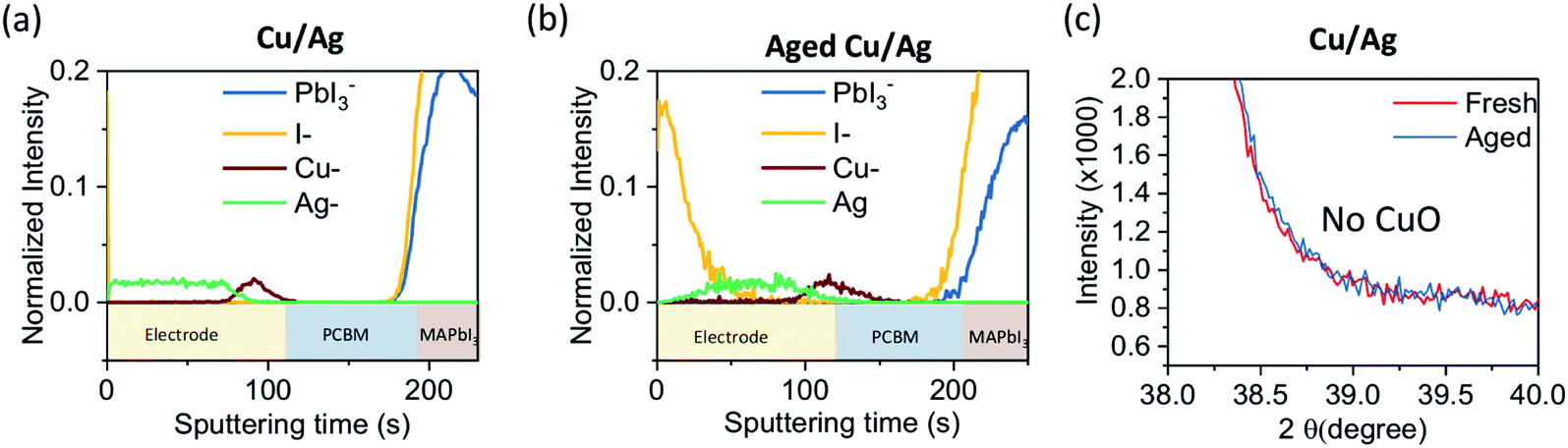 | ||
| Fig. 3 Time-of-flight secondary ion mass spectrometry (ToF-SIMS) depth profile of device with (a) Cu–Ag (b) aged Cu–Ag electrode. (c) XRD spectra of Cu–Ag electrode on device before and after ageing. The devices are aged under same condition as Fig. 1d. | ||
 | ||
| Fig. 4 Schematic diagram of aged devices with (a) Ag (b) Cu and (c) Cu–Ag counter electrode. | ||
Age induced structural transitions
While the Cu–Ag bilayer configuration demonstrated better improved to both oxidation and metal–halide formation at the ETL–electrode interface, a gradual reduction in PCE over time is still observed. Naturally, such devices are not immune to the inherent instability and degradation of the perovskite layer but do offer improved resistance to both. Thus far we have focused on diffusion and oxidation as the origins of diminished performance over time, we now turn to consider structural changes that may also be occurring in the perovskite active layer with ageing. In addition to compositional changes caused by ageing structural changes appear also to be induced highlighting the complex interplay between these processes. The XRD patterns for representative fresh and aged devices highlight this phenomenon, Fig. S9.† In the case of Al electrodes near complete degradation is observed, evidenced by a significant reduction in peak intensity and the emergence of a strong PbO2 peak at 30.31° 2θ,43 this is consistent with the J–V data shown in Fig. 1d. However, for the other electrode configurations there is an observed splitting of the (110) diffraction peak around 14.15° 2θ with the emergence of a (002) diffraction peak at 14.03° 2θ. In MAPI system the (110) diffraction peak often displays an asymmetry owing to the overlapping (002) diffraction peak that is anticipated owing to the tetragonal structure being stabilized at room temperature.44 Looking in detail at the (110)/(002) peak splitting, Fig. 5a–c, with the fitting of these two phases is shown in Fig. 5d and e (fitting parameters given in Table S3†) it is apparent that device ageing is having a significant impact on structure and that there is a distinct structural transition occurring during the ageing process. This is more evident as we move to the higher order diffraction peaks, Fig. 5f and g, where more pronounced peak splitting is clearly observed. From the ToF-SIMS data discussed above it is apparent that the MAPI active layer is becoming X-site i.e. iodine deficient during ageing. Looking at the integrated peak areas of the (100) and (002) family of planes their sum appears to be reasonably consistent indicating that the quantity of crystalline material remains fairly constant – this can be interpreted as a transition in structure rather than a degradation of formation of any amorphous phases. It is unclear, and indeed beyond the scope of this work as to whether the iodide diffusion is driving the structural distortion or vice versa and this will be the focus of our continuing studies. | ||
| Fig. 5 XRD patterns of MAPbI3 of devices with (a) Ag (b) Cu (c) Cu–Ag counter electrode before and after ageing under same condition in Fig. 1d. (d–g) The fitting plots of XRD data of MAPbI3 before and after ageing. | ||
Conclusions
In summary, we demonstrate that employing Cu–Ag bilayer electrodes can effectively enhance electrode and device stability compared to single metal electrodes of Cu, Ag and Al. Using ToF-SIMS we identify the nature of the perovskite active layer components that diffuse during extended device ageing under operation and highlight the synergistic relationship in the dual electrode configuration where the Cu layer (10 nm) inhibits AgI formation at the PCBM/electrode interface, and the susceptibility of Cu to oxidation is circumvented by utilizing Ag as a barrier to oxygen. In addition to identifying the diffusing species we also highlight significant structural transition using X-ray diffraction and show how these are enhanced with device ageing under operation. Our new electrode configuration confers numerous advantages on the devices and can be readily implemented during electrode evaporation. Our structural analysis gives an insight into ageing related structural changes that have not thus far been reported and provide an exciting avenue of future exploration in these fascinating energy conversion systems.Experimental details
Perovskite solar cell fabrication
The inverted (p–i–n) planar structure perovskite solar cells consisted of ITO/PTAA/PFN/perovskite/PCBM/BCP/top electrode. The top electrode was varied as described in the manuscript. The devices were fabricated by firstly cleaning ITO substrates in acetone, soap, water, acetone and then isopropanol using ultrasonics, drying under a N2 stream and finally exposing to UV-ozone treatment immediately before use. PTAA (2 mg mL−1 in chlorobenzene) was spin-coated onto the cleaned ITO substrate at 3000 rpm for 20 seconds. The perovskite solution, 1.5 M MAPbI3 in DMF/DMSO (8.9![[thin space (1/6-em)]](https://www.rsc.org/images/entities/char_2009.gif) :1.1), was then spin-coated on the substrate at 4000 rpm for 30 seconds. After 7 seconds of spinning 0.4 mL diethyl ether was dripped onto the substrate. The substrate was then annealed at 60 °C for 1 minute and then 100 °C for 30 minutes. PCBM solution (30 mg mL−1) was spin-coated on the substrate at 2000 rpm for 20 seconds. BCP (0.5 mg mL−1) was then spin coated on the substrate at 4000 rpm for 20 seconds. Finally, 100 nm of Al, Ag or Cu was thermally evaporated as a top electrode, in the case of bilayer electrodes 10 nm Cu and 100 nm Ag were thermally evaporated in sequence without breaking vacuum.
:1.1), was then spin-coated on the substrate at 4000 rpm for 30 seconds. After 7 seconds of spinning 0.4 mL diethyl ether was dripped onto the substrate. The substrate was then annealed at 60 °C for 1 minute and then 100 °C for 30 minutes. PCBM solution (30 mg mL−1) was spin-coated on the substrate at 2000 rpm for 20 seconds. BCP (0.5 mg mL−1) was then spin coated on the substrate at 4000 rpm for 20 seconds. Finally, 100 nm of Al, Ag or Cu was thermally evaporated as a top electrode, in the case of bilayer electrodes 10 nm Cu and 100 nm Ag were thermally evaporated in sequence without breaking vacuum.
Device characterization and stability measurements
The J–V characteristics were measured under Air Mass 1.5G global (AM 1.5G) illumination (Xenon lamp) at 1 sun intensity, calibrated by a certificated silicon reference cell from National Renewable Energy Laboratory (NREL). The device stability measurements were performed in ambient air under 1 sun illumination provided by an LED light source. The intensity of the LED light was calibrated by matching the Jsc of devices measured using the xenon lamp. The devices were loaded at 0.8 V, which is close to maximum power point, and their J–V characteristics measured every 5 hours.Scanning electron microscopy (SEM)
A LEO Gemini 1525 Field Emission Scanning Electron Microscope was used to obtain SEM images. The sample was coated with 5 nm chromium. Working distance was set at 5 mm, with the accelerating voltage kept below 5 kV.XRD measurements
X-ray diffraction (XRD) profiles of perovskite films were obtained with a X'Pert Powder diffractometer (PANalytical) using K line of Cu X-ray source. The diffraction patterns cover a 2θ range of 10–50°, with a step size of 0.016°.SIMS
ToF-SIMS was performed using the IONTOF-TOFSIMS5 instrument. An O2 1 kV (∼230 nA) sputter beam, with a raster size of 300 μm × 300 μm, for its uniform sputtering rates and minimization of damage accumulation, was used. For the generation of secondary ions, a Bi3+ 25 kV (∼0.5 pA) primary ion beam in the high-current bunched mode (HCBM) for higher mass resolution was used, in which a 150 μm × 150 μm analysis area was centered within the sputter crater. Measurements were performed in the interlaced mode (no pause between sputtering and analysis cycles)-total ion images were closely observed to ensure no sample charging took place. The same mass calibration and mass fragment peak list were applied to all mass spectra and depth profiles, respectively, before analysis.Conflicts of interest
There are no conflicts of interest to declare.Acknowledgements
We thank the Global Research Laboratory (GRL) Program through the National Research Foundation of Korea (NRF) funded by the Ministry of Science and ICT (NRF-2017K1A1A2013153) and the EPSRC Plastic Electronics CDT (EP/L016702/1). T. J. M. would like to thank the Royal Commission for the Exhibition of 1851 for their financial support through an 1851 Research Fellowship.References
- W. S. Yang, B. W. Park, E. H. Jung, N. J. Jeon, Y. C. Kim, D. U. Lee, S. S. Shin, J. Seo, E. K. Kim, J. H. Noh and S. Il Seok, Science, 2017, 356, 1376–1379 CrossRef CAS PubMed.
- M. Saliba, T. Matsui, J. Y. Seo, K. Domanski, J. P. Correa-Baena, M. K. Nazeeruddin, S. M. Zakeeruddin, W. Tress, A. Abate, A. Hagfeldt and M. Grätzel, Energy Environ. Sci., 2016, 9, 1989–1997 RSC.
- NREL, Natl. Renew. Enery Lab., 2019, 0923, http://https://www.nrel.gov/pv/cell-efficiency.html.
- M. Kam, Y. Zhu, D. Zhang, L. Gu, J. Chen and Z. Fan, Sol. RRL, 2019, 3, 1900050 CrossRef.
- D. Bi, W. Tress, M. I. Dar, P. Gao, J. Luo, C. Renevier, K. Schenk, A. Abate, F. Giordano, J.-P. Correa Baena, J.-D. Decoppet, S. M. Zakeeruddin, M. K. Nazeeruddin, M. Grätzel and A. Hagfeldt, Sci. Adv., 2016, 2, e1501170 CrossRef PubMed.
- T. Du, J. Kim, J. Ngiam, S. Xu, P. R. F. Barnes, J. R. Durrant and M. A. McLachlan, Adv. Funct. Mater., 2018, 2, 1801808 CrossRef.
- J. Burschka, N. Pellet, S.-J. Moon, R. Humphry-Baker, P. Gao, M. K. Nazeeruddin and M. Gratzel, Nature, 2013, 499, 316–319 CrossRef CAS PubMed.
- T. Du, C. H. Burgess, C.-T. Lin, F. Eisner, J. Kim, S. Xu, H. Kang, J. R. Durrant and M. A. McLachlan, Adv. Funct. Mater., 2018, 28, 1803943 CrossRef.
- X. Zheng, B. Chen, J. Dai, Y. Fang, Y. Bai, Y. Lin, H. Wei, X. C. Zeng and J. Huang, Nat. Energy, 2017, 2, 17102 CrossRef CAS.
- Q. Jiang, Y. Zhao, X. Zhang, X. Yang, Y. Chen, Z. Chu, Q. Ye, X. Li, Z. Yin and J. You, Nat. Photonics, 2019, 13, 460–466 CrossRef CAS.
- C. Lin, J. Lee, J. Kim, T. J. Macdonald, J. Ngiam, B. Xu, M. Daboczi, W. Xu, S. Pont, B. Park, H. Kang, J. Kim, D. J. Payne, K. Lee, J. R. Durrant and M. A. McLachlan, Adv. Funct. Mater., 2019, 1906763 Search PubMed.
- F. Gao, Y. Zhao, X. Zhang and J. You, Adv. Energy Mater., 2019, 1902650 Search PubMed.
- N. Wijeyasinghe, A. Regoutz, F. Eisner, T. Du, L. Tsetseris, Y. H. Lin, H. Faber, P. Pattanasattayavong, J. Li, F. Yan, M. A. McLachlan, D. J. Payne, M. Heeney and T. D. Anthopoulos, Adv. Funct. Mater., 2017, 27(35), 1701818 CrossRef.
- T. Du, W. Xu, M. Daboczi, J. Kim, S. Xu, C.-T. Lin, H. Kang, K. Lee, M. J. Heeney, J.-S. Kim, J. R. Durrant and M. A. McLachlan, J. Mater. Chem. A, 2019, 7, 18971–18979 RSC.
- J. P. Correa Baena, L. Steier, W. Tress, M. Saliba, S. Neutzner, T. Matsui, F. Giordano, T. J. Jacobsson, A. R. Srimath Kandada, S. M. Zakeeruddin, A. Petrozza, A. Abate, M. K. Nazeeruddin, M. Grätzel and A. Hagfeldt, Energy Environ. Sci., 2015, 8, 2928–2934 RSC.
- T. J. Macdonald, M. Batmunkh, C. Lin, J. Kim, D. D. Tune, F. Amboz, X. Li, S. Xu, C. Sol, I. Papakonstantinou, M. A. McLachlan, I. P. Parkin, J. G. Shapter and J. R. Durrant, Small Methods, 2019, 1900164 CrossRef CAS.
- T. Leijtens, K. Bush, R. Cheacharoen, R. Beal, A. Bowring and M. D. McGehee, J. Mater. Chem. A, 2017, 5, 11483–11500 RSC.
- A. M. A. Leguy, Y. Hu, M. Campoy-Quiles, M. I. Alonso, O. J. Weber, P. Azarhoosh, M. van Schilfgaarde, M. T. Weller, T. Bein, J. Nelson, P. Docampo and P. R. F. Barnes, Chem. Mater., 2015, 27, 3397–3407 CrossRef CAS.
- N. Aristidou, I. Sanchez-Molina, T. Chotchuangchutchaval, M. Brown, L. Martinez, T. Rath and S. A. Haque, Angew. Chem., Int. Ed., 2015, 54(28), 8208–8212 CrossRef CAS PubMed.
- N. Aristidou, C. Eames, I. Sanchez-Molina, X. Bu, J. Kosco, M. Saiful Islam and S. A. Haque, Nat. Commun., 2017, 8, 15218 CrossRef PubMed.
- R. Cheacharoen, N. Rolston, D. Harwood, K. A. Bush, R. H. Dauskardt and M. D. McGehee, Energy Environ. Sci., 2018, 11, 144–150 RSC.
- M. D. Kempe, A. A. Dameron and M. O. Reese, Progress in Photovoltaics: Research and Applications, 2014, 22, 1159–1171 CrossRef CAS.
- S. Pont, D. Bryant, C.-T. Lin, N. Aristidou, S. Wheeler, X. Ma, R. Godin, S. A. Haque and J. R. Durrant, J. Mater. Chem. A, 2017, 5, 9553–9560 RSC.
- C.-T. Lin, S. Pont, J. Kim, T. Du, S. Xu, X. Li, D. Bryant, M. A. McLachlan and J. R. Durrant, Sustainable Energy Fuels, 2018, 2, 1686–1692 RSC.
- Y. Bai, Q. Dong, Y. Shao, Y. Deng, Q. Wang, L. Shen, D. Wang, W. Wei and J. Huang, Nat. Commun., 2016, 7, 1–9 Search PubMed.
- C.-T. Lin, F. De Rossi, J. Kim, J. Baker, J. Ngiam, B. Xu, S. Pont, N. Aristidou, S. A. Haque, T. Watson, M. A. McLachlan and J. R. Durrant, J. Mater. Chem. A, 2019, 7, 3006–3011 RSC.
- M. Jorgensen, K. Norrman and F. C. Krebs, Sol. Energy Mater. Sol. Cells, 2008, 92, 686–714 CrossRef.
- Y. Kato, L. K. Ono, M. V. Lee, S. Wang, S. R. Raga and Y. Qi, Adv. Mater. Interfaces, 2015, 2, 2–7 Search PubMed.
- J. Zhao, X. Zheng, Y. Deng, T. Li, Y. Shao, A. Gruverman, J. Shield and J. Huang, Energy Environ. Sci., 2016, 9, 3650–3656 RSC.
- H. Lee and C. Lee, Adv. Energy Mater., 2018, 8, 1–9 Search PubMed.
- K. Domanski, J. P. Correa-Baena, N. Mine, M. K. Nazeeruddin, A. Abate, M. Saliba, W. Tress, A. Hagfeldt and M. Grätzel, ACS Nano, 2016, 10, 6306–6314 CrossRef CAS PubMed.
- S. Seo, S. Jeong, C. Bae, N. G. Park and H. Shin, Adv. Mater., 2018, 30, 1–8 Search PubMed.
- K. O. Brinkmann, J. Zhao, N. Pourdavoud, T. Becker, T. Hu, S. Olthof, K. Meerholz, L. Hoffmann, T. Gahlmann, R. Heiderhoff, M. F. Oszajca, N. A. Luechinger, D. Rogalla, Y. Chen, B. Cheng and T. Riedl, Nat. Commun., 2017, 8, 1–9 CrossRef PubMed.
- E. Bi, H. Chen, F. Xie, Y. Wu, W. Chen, Y. Su, A. Islam, M. Grätzel, X. Yang and L. Han, Nat. Commun., 2017, 8, 1–7 CrossRef PubMed.
- H. Back, G. Kim, J. Kim, J. Kong, T. K. Kim, H. Kang, H. Kim, J. Lee, S. Lee and K. Lee, Energy Environ. Sci., 2016, 9, 1258–1263 RSC.
- C. M. Wolff, L. Canil, C. Rehermann, N. L. Nguyen, F. Zu, M. Ralaiarisoa, P. Caprioglio, L. Fiedler, M. Stolterfoht, S. Kogikoski Jr, I. Bald, N. Koch, E. L. Unger, T. Dittrich, A. Abate and D. Neher, ACS Nano, 2020, 15 Search PubMed.
- S. Wu, R. Chen, S. Zhang, B. H. Babu, Y. Yue, H. Zhu, Z. Yang, C. Chen, W. Chen, Y. Huang, S. Fang, T. Liu, L. Han and W. Chen, Nat. Commun., 2019, 10, 1161 CrossRef PubMed.
- J. Xiong, B. Yang, C. Cao, R. Wu, Y. Huang, J. Sun, J. Zhang, C. Liu, S. Tao, Y. Gao and J. Yang, Org. Electron., 2016, 30, 30–35 CrossRef CAS.
- E. M. Sanehira, B. J. Tremolet De Villers, P. Schulz, M. O. Reese, S. Ferrere, K. Zhu, L. Y. Lin, J. J. Berry and J. M. Luther, ACS Energy Lett., 2016, 1, 38–45 CrossRef CAS.
- J. Xiong, B. Yang, C. Cao and R. Wu, Org. Electron., 2016, 30, 30–35 CrossRef CAS.
- CRC Handbook of Chemistry and Physics, Taylor & Francis, 77th edn, 1996 Search PubMed.
- A. De Rooij, The Oxidation of Silver by Atomic Oxygen, 1989, vol. 13 Search PubMed.
- P. Y. Chen, J. Qi, M. T. Klug, X. Dang, P. T. Hammond and A. M. Belcher, Energy Environ. Sci., 2014, 7, 3659–3665 RSC.
- S. Kavadiya, J. Strzalka, D. M. Niedzwiedzki and P. Biswas, J. Mater. Chem. A, 2019, 7, 12790–12799 RSC.
Footnote |
| † Electronic supplementary information (ESI) available. See DOI: 10.1039/d0ta01606c |
| This journal is © The Royal Society of Chemistry 2020 |