
Instability of p–i–n perovskite solar cells under reverse bias†
Ricardo A. Z.
Razera
 ab,
Daniel A.
Jacobs
a,
Fan
Fu‡
a,
Peter
Fiala
a,
Marion
Dussouillez
c,
Florent
Sahli
a,
Terry C. J.
Yang§
a,
Laura
Ding
c,
Arnaud
Walter
a,
Adriano F.
Feil
d,
Henri I.
Boudinov
b,
Sylvain
Nicolay
c,
Christophe
Ballif
ac and
Quentin
Jeangros
*a
ab,
Daniel A.
Jacobs
a,
Fan
Fu‡
a,
Peter
Fiala
a,
Marion
Dussouillez
c,
Florent
Sahli
a,
Terry C. J.
Yang§
a,
Laura
Ding
c,
Arnaud
Walter
a,
Adriano F.
Feil
d,
Henri I.
Boudinov
b,
Sylvain
Nicolay
c,
Christophe
Ballif
ac and
Quentin
Jeangros
*a
aÉcole Polytechnique Fédéral de Lausanne (EPFL), Institute of Microengineering (IMT), Photovoltaics and Thin-Film Electronics Laboratory (PV-Lab), Rue de la Maladière 71b, Neuchâtel 2002, Switzerland. E-mail: quentin.jeangros@epfl.ch
bUniversidade Federal do Rio Grande do Sul (UFRGS), Laboratório de Microelectrônica, Av. Bento Gonçalves 9500, Porto Alegre, RS, Brazil
cCSEM, PV-Center, Jaquet-Droz 1, 2002 Neuchâtel, Switzerland
dPontifícia Universidade Católica do Rio Grande do Sul (PUCRS), Escola de Ciências, Av. Ipiranga, 90619-900, 6681, Porto Alegre, RS, Brazil
First published on 22nd November 2019
Abstract
Partial shading can trigger permanent damage in photovoltaic modules because the illuminated solar cells drive the shaded cells into reverse bias. Under reverse bias conditions, perovskite solar cells have been shown to degrade quickly due to processes that have so far remained elusive. Here, we combine optical, microstructural, and electrical characterization to address the mechanisms governing perovskite solar cell degradation under reverse bias. Three main processes are shown to occur in cesium/formamidinium lead iodide/bromide cells depending on the reverse voltage applied, the duration of the reverse bias treatment and the cell structure. The first and most severe involves the formation of highly conductive shunts, preferentially in regions covered by the metal electrode (with apparently equal propensity for various metals) and, at higher reverse voltages, within the perovskite active area. Second, we find that iodide is reversibly driven into the organic electron transport layer, causing an S-shape in the current–voltage curve and lowering power conversion efficiency. Finally, under heavy reverse biasing the perovskite absorber is shown to degrade into iodide- and bromide-rich sub-layers, an irreversible process associated with a shift in the effective band gap and changes to the perovskite microstructure. Criteria that must be met to pass partial shading tests defined by the International Electrotechnical Commission are also discussed in relation to these issues, indicating the urgent need for device structures far more robust than those usually reported.
1 Introduction
Photovoltaic (PV) modules can become partially shaded during operation in a variety of ways, such as by the shadow of nearby trees and artificial structures; through soiling by sand, snow and bird droppings; and in a more transient fashion during module inspection or cleaning. Under partial shade, some solar cells remain illuminated and continue producing current while shaded cells behave as simple diodes. As solar cells are typically connected in series, the covered cells must pass the current of the illuminated cells but cannot do so without being driven into reverse bias. Depending on the breakdown voltage of the solar cells (defined here as the reverse voltage at which an appreciable current flows through the active, not-shunted regions of the solar cell) and the possible presence of shunts (defined as localized, highly conductive pathways between top and bottom electrodes), all the current produced by the illuminated cells is liable to flow through a small area of the shaded cell(s). The resulting large current densities can cause excessive local heating, damaging the cell and/or the encapsulant, even for silicon technologies.1–5 Additionally, the reverse voltage can trigger degradation processes such as those that are known to affect other thin-film modules.6,7As a testament to the severity of the damage that may be induced by partial shading, the International Electrotechnical Commission (IEC) has set up a reliability protocol to test the partial shading resilience of PV modules.8 Thus, any commercially relevant perovskite technology will have to demonstrate adequate stability under reverse bias conditions. Although the use of bypass diodes can limit the reverse voltage applied on shaded cells,1–3 these add cost to the module, so it is desirable to make the cells themselves as resilient as possible against reverse voltage, thereby minimizing the number of necessary bypass diodes. A first detailed study on the topic of reverse bias stability in perovskite cells was reported recently by Bowring et al.9 The authors demonstrated that both p–i–n and n–i–p perovskite cells degrade quickly under moderate reverse voltages (less than −1 V) with hot spots appearing in just a few minutes. Even in the absence of hot spots, another degradation effect was reported whereby the cell's series resistance increased and the Voc decreased, due to a presumed electrochemical reaction between the perovskite absorber and adjacent layers. However, only indirect evidence was provided for this electrochemical process. The lack of fundamental understanding in this area is clearly hindering progress towards the design of perovskite solar cells exhibiting sufficient stability in reverse bias, as highlighted by Rong et al.10
Here, we combine optical and electrical characterization techniques to directly assess the degradation mechanisms induced by reverse bias in p–i–n perovskite solar cells, i.e. the formation of shunts and interfacial reactions. Furthermore, we highlight the appearance of a previously unidentified effect caused by the application of a reverse bias: current-induced phase segregation. We conclude by analyzing the requirements needed to address these issues in future cell and module designs.
2 Mechanisms of degradation in reverse bias
2.1 Shunt formation
The perovskite composition studied in this work is (FAPbI3)0.83(CsPbBr3)0.17, which has a band gap of 1.64 eV and improved thermal stability compared to compositions containing methylammonium. The cell stack is depicted in Fig. 1a and the fabrication methods are detailed in the ESI.† Current–voltage (I–V) curves of this cell design are shown in Fig. S1.† We focus on the stability of semi-transparent cell stacks deposited in the p–i–n sequence and in which the metal electrode is deposited as fingers on top of a transparent conductive oxide. One advantage of this structure is that it permits simultaneous investigations of stability in regions with and without coverage by the metal electrode. It also mirrors the structure used as a top cell in perovskite/Si or perovskite/perovskite multi-junction cells.11,12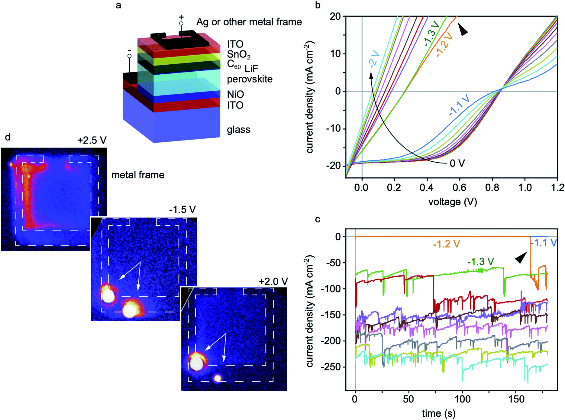 | ||
| Fig. 1 (a) Structure of the cell studied in this work. The “+” and “−” signs indicate that the cell is reverse biased. (b) I–V curves taken immediately after biasing the cell at progressively higher (in absolute value) reverse voltages. (c) Reverse current measured during the 3 min of each reverse biasing step. (d) Left: Thermograph of a fresh cell measured with a forward bias of 2.5 V, middle: same cell imaged at a reverse bias of −1.5 V, showing two new hot spots, and right: same cell under a forward bias of 2 V (after it had been reverse biased at −1.5 V), demonstrating that the shunts that formed in the reverse bias step are still present. | ||
To monitor the reverse bias-induced degradation, we adopted a stress-test whereby the reverse voltage is progressively increased in increments of −0.1 V for 3 minutes per step. After each step, I–V curves are taken first with a forward (−0.1 V to 1.2 V) and then a reverse (1.2 V to −0.1 V) scan to monitor changes in performance. A representative evolution of the I–V curve (forward scans) of a cell using the above protocol is shown in Fig. 1b and S2.† Two processes affecting the shape of the I–V curve are found to occur in succession, irrespective of the direction of the scan (Fig. S3†). For voltages less (in magnitude) than −1.2 V, an S-shape appears, while for higher voltages the cell becomes shunted, as observed from the decrease in Voc and linear I–V characteristics. Fig. 1c reports the reverse current that flows through the cell at each reverse bias step. It is seen that, for this sample, the reverse current remains negligible (less than 1 mA cm−2) for reverse voltages up to −1.1 V. However, after nearly 3 minutes at −1.2 V, the current increases abruptly to more than 50 mA cm−2 in magnitude, signaling the formation of one or more shunts. In addition, burst noise, typical of metal precipitates inside semiconductor devices,13 appears at this point in the current signal.
To verify that shunts are indeed forming under reverse bias, fresh devices were analyzed by dark lock-in thermography.14 These devices were first driven with a forward bias of 2.5 V, with the resulting thermograph exhibiting no hot spots (top left panel of Fig. 1d). This initial test confirms that no significant shunts were present in the fresh state. Subsequently, exposing the cell to a reverse voltage of −1.5 V (1![[thin space (1/6-em)]](https://www.rsc.org/images/entities/char_2009.gif) :1 on-off duty-cycle at 25 Hz) was found to induce the formation of hot spots at the position of the Ag frame (middle panel in Fig. 1d). When driving the cell again in forward bias (bottom right thermograph in Fig. 1d), the two hot spots remained, indicating that these shunts were formed during the reverse bias treatment and that the cell remained shunted when the reverse bias was removed.
:1 on-off duty-cycle at 25 Hz) was found to induce the formation of hot spots at the position of the Ag frame (middle panel in Fig. 1d). When driving the cell again in forward bias (bottom right thermograph in Fig. 1d), the two hot spots remained, indicating that these shunts were formed during the reverse bias treatment and that the cell remained shunted when the reverse bias was removed.
For cells stressed up to voltages of −5 V instead of −2 V, shunts at the position of the metal electrode became severe enough for burn marks to be visible by the naked eye, as shown in Fig. S4a.† In fact, the metallic shunts could be seen from the glass side in the regions of the burn marks. Once the shunts are formed, the high power dissipated in these regions quickly degrades the absorber (which becomes porous with Pb-rich bright inclusions) and the Ag electrode (which clusters in some regions) as highlighted by the scanning electron microscopy images shown in Fig. S4b and c.† Noticeably, cells featuring Cu or a Ni/Al stack as top electrode in place of Ag showed similar shunting behaviour (Fig. S5†). Regular opaque cells, with a metal electrode deposited directly on top of the electron transport layer (C60 here) were also tested. Their stability in reverse bias was found to be even worse with shunts forming at reverse voltages as low as −0.3 V (Fig. S6†).
Several processes may explain the formation of shunts at the position of the metal electrode. First of all, bias-induced migration of Ag and other metals (including Au) has been observed in several studies which investigated the operational stability of perovskite solar cells (in forward bias conditions).15,16 One possibility is that such metal migration also occurs in reverse bias, resulting in the formation of metallic filaments within the perovskite layer in a manner analogous to that proposed for memristive devices.17 Indeed, under reverse bias, the polarity of the applied potential in p–i–n devices may drive positively charged metal ions through the ITO, SnO2 and perovskite layers to the opposing electrode.
However, a metal electrode is apparently not necessary to observe reverse shunting behaviour in perovskite cells. Indeed, as observed by Bowring et al.,9 devices with only ITO as a rear contact (no metal fingers) were also found to develop shunts under reverse bias, although this time at lower voltages of about −3 V (Fig. S7†). Complementary to the phenomenon of metal migration, this finding points to a limited stability of the perovskite layer itself under reverse bias, which may occur due to a destabilizing accumulation of mobile ions or a significant loss of iodide, resulting finally in the formation of metallic Pb which shorts the two electrodes. In contrast with metal migration, this mechanism will be relevant to the reverse-bias stability of all cell architectures, including those based on the n–i–p polarity.
2.2 S-shape development
Prior to electrode shunting, an S-shape in the I–V curve is observed to form with increasing severity as the reverse pre-biasing increases (Fig. 1b). The relation to voltage pre-biasing and similarity to I–V curves reported in several modelling studies of hysteresis18–20 suggests that the effect is likely related to ion migration. However, one notable difference here is that the open-circuit voltage remains remarkably constant with increasing exposure to negative voltages, by contrast with most observations in the context of hysteresis. This is suggestive of a process that affects charge transport but has a minimal effect on recombination.To assess the mechanism associated with the S-shape formation, reverse-biased solar cells were investigated using scanning transmission electron microscopy (STEM) coupled to energy dispersive X-ray (EDX) spectroscopy. Fig. 2a shows a STEM high-angle annular dark-field (HAADF) image of the cross-section of a cell, in a region far from the metal electrode, that was reverse biased up to −5 V using the protocol described above.
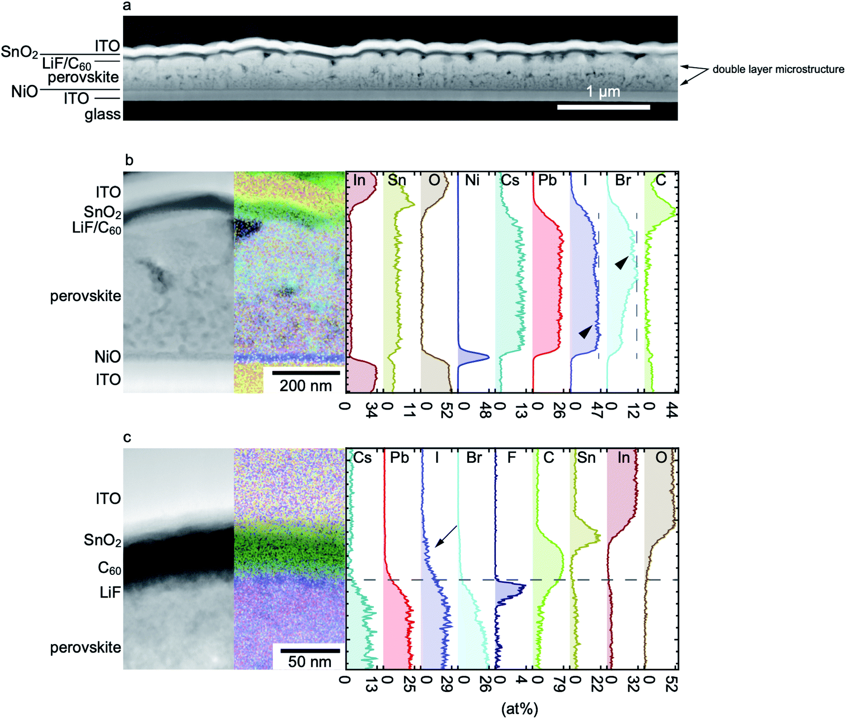 | ||
| Fig. 2 (a) Scanning transmission electron microscopy (STEM) high-angle annular dark-field (HAADF) image of a solar cell degraded at −5 V, showing large voids and a double layer structure. (b) STEM HAADF image of the cell shown in (a) superimposed on its right side with its corresponding EDX chemical map and corresponding concentration profile quantified using the Cliff–Lorimer method.21 As indicated by arrowheads, the Br concentration increases in the upper part of the absorber, while an inverse trend is noticed for I. The Sn signal inside the PK layer is an artifact of the quantification procedure. (c) STEM HAADF image and corresponding EDX chemical map and concentration profile of a sample with a higher Br content taken in the region close to the perovskite/LiF/C60 interface, which highlights the migration of iodide into the C60 layer during reverse biasing (arrowed). | ||
Apart from the formation of large voids indicative of a loss of material during either the biasing experiments or during the TEM sample preparation by focused ion beam (FIB), the biased cell exhibits a double layer microstructure, with a relatively smooth top layer (adjacent to the n-type electrode) and a rough bottom layer. For comparison, a STEM image of an as-deposited reference cell is shown in Fig. S8.† The reference cell also exhibits some voids, although of a smaller size and likely induced by the FIB preparation, but no double layer structure, confirming that the latter feature is caused by the reverse bias treatment. The EDX chemical map and atomic concentration profile shown in Fig. 2b of the reverse biased cell also show that the top and bottom layers have different Br concentration. This is evidence of bias-induced phase segregation and will be discussed further in the next section, but does not provide an immediate explanation for the formation of the S-shape.
The magnified view of the perovskite/LiF/C60 interface shown in Fig. 2c provides a more suggestive explanation of the I–V characteristics seen in Fig. 1. Iodine is seen to have migrated beyond the LiF and into the C60 layer following reverse bias by comparison with the unbiased reference (Fig. S8†). On the other hand, the Cs, Pb and Br EDX signals do not extend as far across the same interface (note that some overlap between the different layers is induced by projection effects, as the perovskite layer exhibits some roughness and the TEM sample is about 100 nm thick). Iodine is likely driven into the C60 in its ionized form (I−) since a positive voltage is applied on the C60 side under reverse bias. Voltage-driven halide migration into an organic selective contact (Spiro-OMeTAD or C60 depending on the polarity of the bias) was also observed in a previous study employing in situ TEM.22 One possible explanation for the S-shape behaviour is therefore that iodide acts as p-type dopant in C60, as reported for I2 in several organic semiconductors such as pentacene,23 or that it simply charge compensates the n-type doping resulting in a reduced carrier density. In the latter case, carrier densities may be reduced to the point where transport is no longer ohmic and instead occurs in the (non-linear) space-charge-limited current regime.24
The formation of S-shaped I–V curves following reverse bias appears to be reversible to some extent. To investigate this, solar cells without metal on their front electrodes were fabricated in order to avoid the issue of electrode shunting. These cells were then reverse biased according to the stress-testing procedure described above. As shown in Fig. 3a, the absence of metal indeed prevents the formation of ohmic shunts when the cell is stressed up to −2 V. Without their masking effect on the I–V curve, it is seen that the S-shape gets progressively more severe as the reverse voltage is increased. After reverse biasing, the metal electrode-free cell was submitted to maximum power point tracking (MPPT) for about 1 h and, as shown in Fig. 3b, the efficiency recovered to its initial value of about 7.3% (a low value caused by a high series resistance due to the absence of a metal electrode). Fig. 3c shows a comparison between the I–V curves before and after degradation, and after recovery. The initial and recovered I–V curves almost overlap in the power-generating quadrant, with only a small decrease in the current injection beyond Voc. Notably, cells were found to recover even when left in the dark, although at a slower rate than with MPPT.
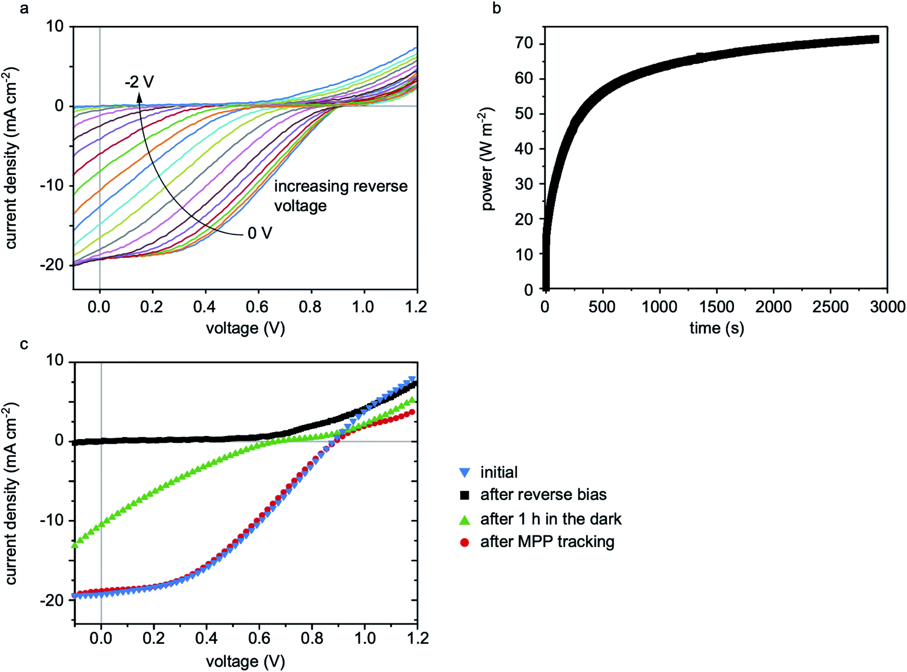 | ||
| Fig. 3 (a) I–V curves of a cell without any metal electrode taken after progressively increasing the absolute value of the reverse bias. While a severe S-shape builds up, no shunts appear. (b) Maximum power point tracking of the same cell after degradation, showing that the efficiency recovers. (c) Comparison of the I–V curves of the same cell in its fresh state, immediately after reverse biasing, after 1 h in the dark and after maximum power point tracking. | ||
To further support the suggestion that it is the iodine inside the C60 layer that is causing the S-shapes in Fig. 1b and 3a, EDX maps of a recovered metal electrode-free solar cell were acquired. As shown in Fig. S9,† no iodine signal was found inside the C60 layer for a recovered solar cell, strengthening our hypothesis.
While the S-shape can be reversed (at least to some extent), the introduction of thin layers directly on the perovskite surfaces (e.g. Al2O3 deposited via ALD) may prevent iodide from leaking into the organic charge carrier-selective layer and hence any modification to its charge extraction capabilities.25,26
2.3 Phase segregation
The segregation of mixed halide perovskites into I-rich (low bandgap) and Br-rich (high bandgap) regions was first reported by Hoke et al.27 Since then, significant progress has been made in identifying the causes and implications of this phenomenon.28–34 Although some factors remain unclear,32,34 it has been shown that this effect is intimately linked to the presence of excess free carriers in the perovskite, whether by photogeneration or electrical injection.33Here, direct evidence of reverse bias-induced phase segregation was obtained using electron microscopy (Fig. 2b). The sample investigated by STEM EDX experienced a reverse bias of −5 V, a voltage significantly below the breakdown voltage, denoted hereafter as −Vbd, (Vbd ≈ 1–1.5 V, Fig. S10†). Consequently, a high current passed through the cell (about 1 A cm−2), likely inducing this phase segregation. The steady state photoluminescence (PL) spectra shown in Fig. 4a are further indications of the phase segregation induced by this current injection. For this experiment, a fresh device was reverse biased at −3 V for 15 min and then the PL signal was measured from both sides of the sample (excitation wavelength of 514 nm corresponding to an absorption depth of about 120 nm). A red-shift of about 0.02 eV in bandgap is observed according to the luminescence measured from the NiO side, as would be expected given the I-rich region observed in the STEM EDX data (Fig. 2b). By contrast, a slight blue-shift (approximately 0.005 eV) was measured from the C60 side, also in accordance with the EDX data. The PL laser on its own was also able to induce shifts in the bandgap, but only if a high enough photon dosage was provided with either high intensity or long exposure times. To investigate the bias-induced segregation alone, the exposure time (10 s) and intensity (1 sun) of the PL laser were chosen so that no shift was observable whilst acquiring the spectra, as demonstrated in Fig. S11.†
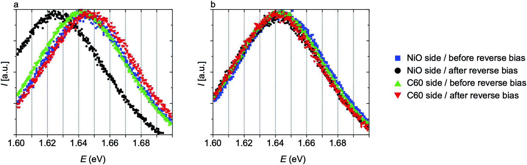 | ||
| Fig. 4 Normalized photoluminescence spectra measured from the NiO and C60 sides before and after reverse biasing at (a) −3 V and (b) −0.5 V for 15 min. In (a), a red-shift is measured on the NiO side, while a slight blue-shift is measured on the C60 side, inline with the elemental map of Fig. 2b. No phase segregation is observed in (b) as the applied voltage is lower in absolute value than the breakdown voltage and hence no current flowed through the device. | ||
Phase segregation induced by reverse biasing has not been reported in any prior study to our knowledge, although its occurrence would be expected given the link to carrier-injection in the perovskite. Duong et al.28 observed phase segregation under forward biasing but reported negligible segregation when applying a reverse voltage of −1 V for 12 h. While the Vbd of the cell in that study was not reported, it can be assumed that 1 V was not sufficient to reach breakdown and negligible current was injected in the absorber. A similar situation was recreated in Fig. 4b, which provides the PL data of a sample biased at −0.5 V for 15 min, a voltage below the −Vbd of approximately −0.8 V of this cell (Fig. S10†). No bandgap shift was observed, in agreement with the hypothesis that a significant excess carrier density is required to trigger phase segregation.33
Shifts in luminescence observed with PL are expected to depend not only on the extent of the phase segregation (and therefore on the value of the reverse bias applied to the cell) but also on the diffusion length of the carriers in the device. With short diffusion lengths, the wavelength of emission will be strongly influenced by the location of carrier generation, and hence result in blue-shifted emission when illuminating from the high-bandgap side and red-shifted emission from the low-bandgap side. On the other hand, with long diffusion lengths, all carriers will migrate to the lower bandgap region and emit a low energy photon, irrespective of illumination direction. Indeed, in some cases we observed a red-shift in the perovskite bandgap in the PL spectra obtained from both sides of the device. In Fig. S12,† for example, the PL spectra of a sample degraded at −5 V for 30 min is shown, with an observable red-shift when measuring from both NiO and C60 sides. The difference between Fig. 4a and S10† is indicative of a difference in carrier lifetimes and size of the segregated regions. Presumably, the sample degraded at −5 V for 30 min had a thicker I-rich layer, which would translate into carriers being able to reach the lower bandgap region even when the light is shone from the C60 side.
It is natural to consider that the S-shape discussed in the previous section might be a side-effect of the phase segregation, given that both phenomena are caused by reverse bias. We ruled this out by measuring the PL of samples that presented an S-shaped I–V curve. In Fig. S13,† we show the PL of the sample for which the I–V curves after reverse bias treatments are shown in Fig. 3a. No observable shift in the peak position was found. Furthermore, no significant current flowed through the sample during these treatments, as shown in Fig. S13.† Therefore, it seems that this sample did not phase segregate, even though it had an S-shaped I–V curve after reverse biasing. These observations indicate separate mechanisms for the two effects and reinforce our hypothesis that the S-shapes result rather from migration of iodide into the C60 layer.
While an injection of charges is required to trigger phase segregation in reverse bias, in accordance with mechanisms proposed to be the cause of light-induced phase segregation,31,33 there are several differences between our observations and the light-induced phase segregation process first reported by Hoke et al.27 For example, as noted above in relation to Fig. 2, the phase segregation induced by reverse bias results in a double layer structure within the perovskite layer with fairly uniform characteristics along the cell's lateral dimensions. This differs from the heterogeneous nucleation of iodine-rich domains observed under illumination by cathodoluminescence.31 Another notable difference between the segregation driven by reverse bias as opposed to light concerns the kinetics of the process.33 The images shown in Fig. 2 were acquired at a delay of one week after stress-testing the cells, so it is clear that bias-induced segregation lacks the reversibility of its light-driven counterpart (wherein segregation is often found to revert on a timescale of minutes to hours30,32). PL shifts also persisted for one week after reverse biasing (Fig. S14†). Notably, previous reports on current-induced phase segregation did not mention if the effect is reversible.28,33 The difference in the self-diffusion rate that reverses the segregation may be related to the microstructural changes observed in our samples, in particular the irreversible appearance of a double layer microstructure (Fig. 2b and S8†).
Bowring et al.9 did not mention any phase segregation effect in their study on the reverse bias stability of (FAPbI3)0.83(CsPbBr3)0.17 cells. However, they did report I–V curves of a sample first degraded in the dark with a current of −Impp and then recovered at MPPT for 3 h. The I–V curve after recovery had a Jsc higher by at least 2 mA cm−2 and a Voc lower by about 100 mV compared to before degradation. While the Voc loss may be explained by an increase in bulk and/or surface recombination, the increase in Jsc is more difficult to explain without invoking a decrease in apparent bandgap (triggered by phase segregation). While not discussed explicitly, phase segregation is therefore consistent with their experiments as well. Furthermore, this speculation would indicate that reverse bias-induced phase segregation is not recoverable even after 3 h of MPPT, in agreement with our STEM EDX observation of irreversibly phase segregated layers.
Fig. 5 presents a summary of the degradation mechanisms observed in this work as a function of the reverse voltage range at which they occur, i.e. shunt formation at the position of the metal electrode and within the active area, S-shape due to iodine migration in the C60 and phase segregation.
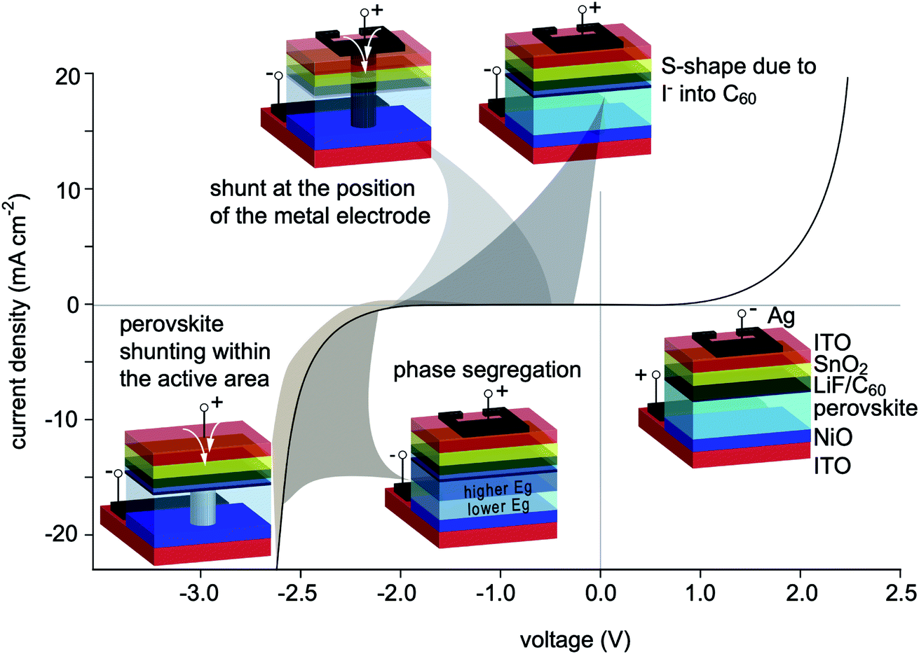 | ||
| Fig. 5 Summary of the degradation mechanisms occurring during reverse biasing as a function of the voltage range in which they occur. In this example, the breakdown voltage is ≈−2 V, but in practice this value may range between −1 V and −4 V depending on solar cell design and processing conditions. The reverse voltages at which the mechanisms described here occur also depend on the cell design. The mechanisms are: (1) halogens being driven inside the C60 layer, which in our samples occurred for any reverse voltage applied; (2) shunt formation, which is voltage driven and becomes dominant for voltages higher than about −0.5 V, with shunts forming preferentially at the position of the metal electrode but also within the active area of the cell at higher voltages; (3) phase segregation, which only occurs at voltages higher than the breakdown voltage, when current starts to flow through the perovskite. | ||
3 Module design implications
We next discuss the criteria that must be satisfied in order to pass the IEC partial shading test mentioned in the introduction. The test consists of two parts: first, the cell with the highest leakage current in the module is identified. Then, the module is illuminated at 1000 W m−2 with a AM1.5G spectrum under short-circuit while the previously identified cell is shaded, inducing a reverse bias that depends on the cell's breakdown voltage, the number of bypass diodes in the module and the number of solar cells that are still illuminated. Although the test provides a standard protocol for testing photovoltaic modules in partial shading conditions, it does not provide a quantitative pass/fail criterion for the power loss,8 complicating any critical assessment. As an example of how such tests will need to be adapted to the unique complexity of perovskite cells, Bowring et al.9 observed that each cycle of reverse bias degradation-recovery at MPP yields a slower recovery rate. How such an effect could be incorporated into a reverse bias testing protocol has yet to be determined. For the present discussion we therefore restrict attention to the irreversible effects induced by the formation of shunts, current-induced phase segregation and changes in microstructure.Assuming first that no bypass diodes are used in the PV module, the highest (in magnitude) reverse voltage applied to the shaded cell is Vbd and the maximum reverse current will be that produced by the illuminated cells, Impp. The breakdown voltage therefore has a strong influence on the reverse bias stability of perovskite solar cells since it determines the maximum reverse voltage that can be applied before a reverse current starts to flow through the device. It follows that, without bypass diodes, lowering Vbd may alleviate shunting problems (Fig. 1b–d) by reducing the reverse voltage applied to the shaded solar cell and also alleviate thermal degradation of the perovskite absorber layer by reducing the power dissipated (Impp × Vbd). In this scenario, Vbd must be engineered to less than about 1 V for semitransparent cells, since at −1.2 V we clearly observe severe shunting, even for less than 3 minutes of exposure to reverse bias (Fig. 1b). Our opaque solar cells, on the other hand, would need a Vbd less than 0.3 V (Fig. S6†), which seems highly implausible. Furthermore, even if the power dissipated is low, without bypass diodes the perovskite layer must be stable against current-driven mechanisms such as phase segregation, at least up to Impp.
Alternatively, if these conditions cannot be met, it becomes necessary to employ bypass diodes. A high Vbd becomes beneficial in this case in order to minimize the number of necessary bypass diodes and, consequently, module cost. The reverse voltage Vrev applied on a shaded solar cell when there are N cells per bypass diode, assuming all the other solar cells in the substring are fully illuminated, can be estimated as follows:
| Vrev = (N − 1)Vmpp + Vbp | (1) |
4 Conclusion
Perovskite solar cells are shown to degrade as a result of various mechanisms when a reverse voltage is applied. Two of these mechanisms are irreversible for the cell design studied in this work, with one being related to voltage-driven shunting mechanisms. The second one involves phase segregation accompanied by microstructural changes, which starts when current flows through the cell. The third mechanism, which appears as an S-shape, seems to stem from the migration of iodide from the perovskite into the C60. This last mechanism is reversible to some extent when subjecting the cell to extended maximum power point tracking (∼1 hour). The implications of these observations for the number of bypass diodes and the engineering of the breakdown of the cell to minimize damage in reverse bias have been discussed. Overall, these results highlight the urgent need to develop cell designs that are far more robust to partial shading conditions compared to current state-of-the-art devices. The formation of shunts at the position of the metal electrode, irrespective of the metal employed, and within the active area appears especially problematic and should motivate further research effort.Authors contributions
R. R. and Q. J. designed and performed the experiments and, with the help of D. J., analyzed the data. R. R. made the devices, with the help of F. F., M. D., F. S., L. D. and A. W., who deposited some of the thin film layers. P. F. and T. C. J. Y. provided support with respect to sample characterization. S. N., A. F. F., H. B., C. B. and Q. J. supervised different parts of the work. R. R., D. J. and Q. J. wrote the manuscript with support from all co-authors.Conflicts of interest
There are no conflicts to declare.Acknowledgements
Financial supports from the Swiss Government Excellence Scholarship, the Swiss Federal Office of Energy (SI/501804-01 INTENT), the Swiss National Science Foundation (176552 Bridge Power, CRSII5_171000 Sinergia Episode), the Marie Sklodowska-Curie Individual Fellowship from the European Union Horizon 2020 Research and Innovation Program (747221 POSITS) are gratefully acknowledged.Notes and references
- A. Reinders, P. Verlinden, W. Van Sark and A. Freundlich, Photovoltaic Solar Energy: From Fundamentals to Applications, Wiley, 2017 Search PubMed.
- S. Daliento, F. Di Napoli, P. Guerriero and V. d'Alessandro, Sol. Energy, 2016, 134, 211–218 CrossRef.
- B. Pannebakker, A. de Waal and W. van Sark, Prog. Photovoltaics, 2017, 25, 836–849 CAS.
- Q. Zhang and Q. Li, Proc. IEEE Photovoltaic Specialists Conf., 2012, p. 1344 Search PubMed.
- A. Woyte, J. Nijs and R. Belmans, Sol. Energy, 2003, 74, 217–233 CrossRef.
- M. Kontges, K. Kurtz, C. Packard, U. Jahn, K. Berger, K. Kato, T. Friesen, H. Liu and M. Iseghem, Performance and Reliability of Photovoltaic Systems, International energy agency technical report, 2014 Search PubMed.
- C. Buerhop and J. Bachmann, J. Phys.: Conf. Ser., 2010, 012089 CrossRef.
- IEC, International Standard – Thin-film terrestrial photovoltaic (PV) modules – Design qualification and type approval, International electrotechnical commission technical report, 2008 Search PubMed.
- A. Bowring, L. Bertoluzzi, B. O'Regan and M. McGehee, Adv. Energy Mater., 2018, 8, 1702365 CrossRef.
- Y. Rong, Y. Hu, A. Mei, H. Tan, M. I. Saidaminov, S. Il Seok, M. D. McGehee, E. H. Sargent and H. Han, Science, 2018, 361, eaat8235 CrossRef PubMed.
- F. Sahli, J. Werner, B. Kamino, M. Brauninger, R. Monnard, B. Paviet-Salomon, L. Barraud, L. Ding, J. Leon, D. Sacchetto, G. Cattaneo, M. Despeisse, M. Boccard, S. Nicolay, Q. Jeangros, B. Niesen and C. Ballif, Nat. Mater., 2018, 17, 820–826 CrossRef CAS PubMed.
- A. F. Palmstrom, G. E. Eperon, T. Leijtens, R. Prasanna, S. N. Habisreutinger, W. Nemeth, E. A. Gaulding, S. P. Dunfield, M. Reese, S. Nanayakkara, T. Moot, J. Werner, J. Liu, B. To, S. T. Christensen, M. D. McGehee, M. F. A. M. van Hest, J. M. Luther, J. J. Berry and D. T. Moore, Joule, 2019, 3, 2193–2204 CrossRef CAS.
- S. Hsu, R. Whittier and C. Mead, Solid-State Electron., 1970, 13, 1055–1056 CrossRef.
- O. Breitenstein, J. Bauer, K. Bothe, D. Hinken, J. Muller, W. Kwapil, M. Schubert and W. Warta, IEEE Journal of Photovoltaics, 2011, 1, 159–167 Search PubMed.
- S. Wu, R. Chen, S. Zhang, B. H. Babu, Y. Yue, H. Zhu, Z. Yang, C. Chen, W. Chen, Y. Huang, S. Fang, T. Liu, L. Han and W. Chen, Nat. Commun., 2019, 10, 1161 CrossRef PubMed.
- K. Domanski, J. Correa-Baena, N. Mine, M. Nazeeruddin, A. Abate, M. Saliba, W. Tress, A. Hagfeldt and M. Gratzel, ACS Nano, 2016, 10, 6306 CrossRef CAS PubMed.
- W. Yoo, M. Lyu, J. Yun, C. Kang, Y. Choi and L. Wang, J. Mater. Chem. C, 2016, 4, 7824 RSC.
- W. Tress, N. Marinova, T. Moehl, S. M. Zakeeruddin, M. K. Nazeeruddin and M. Gratzel, Energy Environ. Sci., 2015, 8, 995–1004 RSC.
- P. Calado, A. M. Telford, D. Bryant, X. Li, J. Nelson, B. C. O'Regan and P. R. F. Barnes, Nat. Commun., 2016, 7, 13831 CrossRef CAS PubMed.
- D. Jacobs, Y. Wu, H. Shen, C. Barugkin, F. Beck, T. White, K. Webera and K. Catchpolea, Phys. Chem. Chem. Phys., 2017, 19, 3094 RSC.
- G. Cliff and G. W. Lorimer, J. Microsc., 1975, 103, 203–207 CrossRef.
- Q. Jeangros, M. Duchamp, J. Werner, M. Kruth, R. Dunin-Borkowski, B. Niesen, C. Ballif and A. Hessler-Wyser, Nano Lett., 2016, 16, 7013–7018 CrossRef CAS PubMed.
- B. Lüssem, C. M. Keum, D. Kasemann, B. Naab, Z. Bao and K. Leo, Chem. Rev., 2016, 116, 13714–13751 CrossRef PubMed.
- M. Lampert, Current injection in solids, Academic Press, 1970 Search PubMed.
- B. Chen, P. N. Rudd, S. Yang, Y. Yuan and J. Huang, Chem. Soc. Rev., 2019, 48, 3842–3867 RSC.
- M. Jaysankar, B. A. Raul, J. Bastos, C. Burgess, C. Weijtens, M. Creatore, T. Aernouts, Y. Kuang, R. Gehlhaar, A. Hadipour and J. Poortmans, ACS Energy Lett., 2019, 4, 259–264 CrossRef CAS.
- E. Hoke, D. Slotcavage, E. Dohner, A. Bowring, H. Karunadasa and M. McGehee, Chem. Sci., 2015, 6, 613–617 RSC.
- T. Duong, H. Mulmudi, Y. Wu, X. Fu, H. Shen, J. Peng, N. Wu, H. Nguyen, D. Macdonald, M. Lockrey, T. White, K. Weber and K. Catchpole, ACS Appl. Mater. Interfaces, 2017, 9, 26859–26866 CrossRef CAS PubMed.
- D. W. deQuilettes, W. Zhang, V. M. Burlakov, D. J. Graham, T. Leijtens, A. Osherov, V. Bulović, H. J. Snaith, D. S. Ginger and S. D. Stranks, Nat. Commun., 2016, 7, 11683 CrossRef CAS PubMed.
- S. Draguta, O. Sharia, S. J. Yoon, M. C. Brennan, Y. V. Morozov, J. S. Manser, P. V. Kamat, W. F. Schneider and M. Kuno, Nat. Commun., 2017, 8, 200 CrossRef PubMed.
- C. Bischak, C. Hetherington, H. Wu, S. Aloni, D. Ogletree, D. Limmer and N. Ginsberg, Nano Lett., 2017, 17, 1028–1033 CrossRef CAS PubMed.
- A. Barker, A. Sadhanala, F. Deschler, M. Gandini, S. Senanayak, P. Pearce, E. Mosconi, A. Pearson, Y. Wu, A. Kandada, T. Leijtens, F. De Angelis, S. Dutton, A. Petrozza and R. Friend, ACS Energy Lett., 2017, 2, 1416–1424 CrossRef CAS.
- I. Braly, R. Stoddard, A. Rajagopal, A. Uhl, J. Katahara, A. Jen and H. Hillhouse, ACS Energy Lett., 2017, 2, 1841–1847 CrossRef CAS.
- R. Belisle, K. Bush, L. Bertoluzzi, A. Gold-Parker, M. Toney and M. McGehee, ACS Energy Lett., 2018, 3, 2694–2700 CrossRef CAS.
Footnotes |
| † Electronic supplementary information (ESI) available. See DOI: 10.1039/c9ta12032g |
| ‡ Now at Swiss Federal Laboratories for Materials Science (Empa), Laboratory for Thin Films and Photovoltaics, Ueberlandstrasse 129, 8600 Duebendorf, Switzerland. |
| § Now at CSIRO Energy Centre, 10 Murray Dwyer Circuit, 2304 Mayfield West NSW, Australia. |
| This journal is © The Royal Society of Chemistry 2020 |