
Construction of uniform buried pn junctions on pyramid Si photocathodes using a facile and safe spin-on method for photoelectrochemical water splitting†
He
Li
ab,
Bin
Liu
ab,
Shijia
Feng
ab,
Huimin
Li
ab,
Tuo
Wang
 *ab and
Jinlong
Gong
ab
*ab and
Jinlong
Gong
ab
aKey Laboratory for Green Chemical Technology of Ministry of Education, School of Chemical Engineering and Technology, Tianjin University, Tianjin 300072, China. E-mail: wangtuo@tju.edu.cn
bCollaborative Innovation Center of Chemical Science and Engineering (Tianjin), Tianjin University, Tianjin 300072, China
First published on 26th November 2019
Abstract
Czochralski silicon (p type) with buried pn junctions by surface doping is widely used in photovoltaic (PV) and photoelectrochemical (PEC) water splitting systems. However, phosphorus oxychloride (POCl3) and phosphine (PH3) as phosphorous doping sources that are widely used in industry are of high toxicity. On the other hand, commercially available spin-on dopants (SODs) for laboratory-scale applications are polymer solutions with a large number of phosphorous polymers, leading to a high viscosity. Thus, it is difficult to realize uniform doping on pyramidal surface textured (pyramid) Si substrates using SODs. This study describes the construction of uniform buried pn junctions on pyramid silicon by spin coating ammonium dihydrogen phosphate (ADP) aqueous solution as the phosphorous source, which is of low viscosity and can decompose into P2O5 at high temperatures. Owing to the improved charge carrier separation at the uniform junction, the pn+Si/TiO2/Pt photocathode using low viscosity dopants exhibits a high onset potential of 0.58 V vs. the reversible hydrogen electrode (RHE) and improves the applied bias photon current efficiency from 3.73% (using SOD polymer solution) to 10.6% in 1 M HClO4. When combining the optimized photocathode with a BiVO4 photoanode to form a PEC tandem configuration, a stable solar-to-hydrogen conversion efficiency of 2.09% is achieved under 1 sun illumination.
1. Introduction
With the excessive consumption of non-renewable resources and the deterioration of environmental problems, hydrogen produced from solar-driven photoelectrochemical (PEC) water splitting has attracted wide attention.1–5 Silicon (1.1 eV) is one of the most promising materials among p-type narrow band gap semiconductors (CIGS,6–8 InP,9 Cu2O,10–12etc.) used in PEC water splitting for hydrogen generation because of its earth abundance, high theoretical photocurrent13 and suitable energy band structure for the reduction of protons.14 However, Si suffers from drawbacks such as high reflectivity for planar Si, limited photovoltage, sluggish reaction kinetics and photocorrosion in aqueous solutions.15,16Introducing surface textures into a crystalline Si photoelectrode can effectively reduce light reflection, which has been demonstrated in solid-state photovoltaic solar cells. Furthermore, surface texture provides an enlarged junction area to separate photogenerated hole–electron pairs and a more efficient collection of photogenerated minority carriers.17 The first detailed study on wet etching of Si using a ternary mixture to form pyramidal surface textured (pyramid) morphology was conducted by Price in 1973, which employed sodium or potassium hydroxide (NaOH or KOH), water and isopropyl alcohol.18 With the pyramid morphology, the Si photocathode used in PEC water splitting reached a saturation current density of ∼35 mA cm−2 under simulated sunlight irradiation (AM 1.5G, 100 mW cm−2).19–21 The vapor–liquid–solid (VLS) growth method22 or metal assisted chemical etching (MACE)23 following photolithographic patterning of photoresists was also used to fabricate Si microwire and nanowire arrays, where noble metal Au was normally used with precise control to prevent Si microwire arrays from dumping. However, the enormous area of Si nanowires causes a large number of surface defects, resulting in a significant decrease in saturation photocurrent density and long term stability.24–26 Among these surface morphologies, the pyramid morphology is considered as the most cost-effective, easy-to-manufacture and widely used one. Similar to planar p-Si substrates, band bending is also needed for pyramid substrates to separate photogenerated charge carriers, which is ultimately reflected as photovoltage.
For the sake of obtaining higher photovoltage, buried junctions by surface doping27 still exhibit advantages over many other types of recently reported Si photocathodes, owing to their large barrier height and high quality interface compared with metal–insulator–semiconductor (MIS) structures1,28,29 and p–n heterojunctions,30,31 and more cost-effective when compared with the heterojunction with intrinsic thin-layer (HIT).32
Many doping strategies have been developed to construct buried pn junctions for crystalline Si in PV and PEC fields.27,33–35 For phosphorous diffusion to form pn junctions on p-type Si, one way is to use phosphorus oxychloride (POCl3) or phosphine (PH3) as phosphorus sources, which are widely used in industry. The gaseous POCl3 (or PH3) could uniformly dope pyramid p-Si substrates by supplying a constant and sufficient surface concentration of doping sources. However, both POCl3 and PH3 are of high toxicity,36 requiring complicated doping equipment, which makes them unsuitable for laboratory scale applications. Additionally, owing to the gaseous nature of POCl3 and PH3, it is difficult to fabricate buried junctions on a single side for PEC electrodes due to the double-sided diffusion of gaseous dopants.35 Although single side diffusion can be realized by covering the other side with materials such as photoresists or establishing a diffusion barrier with inert purging gas, the extra steps significantly increase the complexity and cost of the doping process when using POCl3 or PH3 as the doping source. For laboratory scale applications, the spin-on technique is a facile and safe method to distribute liquid dopants uniformly on substrates. The thickness of the as-formed film could be easily controlled by adjusting the spin speed and viscosity of dopants. Nevertheless, commercially available dopants known as spin-on dopants (SODs) are widely used for planar Si substrates,37–40 but they are not compatible with micro features. It is difficult to spin coat SODs on pyramid p-Si substrates uniformly, since SODs are polymer solutions that contain phosphorous polymers with a high viscosity. The non-uniform distribution of the phosphorous dopant on pyramid p-Si substrates would finally result in the different depths of the junction. Therefore, it remains a great challenge to develop a safe and simple process to dope pyramid Si substrates.
This study describes the design and fabrication of a high performance pyramid pn+Si photocathode with uniform buried pn junctions, using a safe and cost-effective spin-on technique. Ammonium dihydrogen phosphate (NH4H2PO4, ADP) aqueous solution of low viscosity that can decompose to phosphorus oxide (P2O5), ammonia and water at high temperatures, rather than the high viscosity SOD polymer solution, was used to uniformly coat the as-prepared pyramid p-Si substrate to form the desired buried junction. The pyramid pn+Si photocathode is further covered by an atomic layer deposition (ALD)-grown TiO2 protective layer and photo-assisted electrodeposited Pt cocatalyst, reaching a 0.58 V vs. the reversible hydrogen electrode (RHE) onset potential and 10.6% applied bias photon-to-current efficiency (ABPE) (2.8 times of that of pyramid pn+Si photocathode doped using SOD polymer solution) in strong acid electrolyte for more than 250 h under simulated AM 1.5G illumination.
2. Results and discussion
2.1 Uniform dopant distribution on pyramid Si from a low viscosity doping source
In this study, a commercially available spin-on dopant (details in the ESI†) consisting of phosphorous polymers, alcohol and water was used as the representative SOD polymer solution, which has been adopted by many previous studies.41,42 On the other hand, water soluble phosphates (such as ADP) could be another group of suitable phosphorous sources. ADP could decompose into P2O5, which could be further reduced to phosphorous by silicon substrates, serving as the dopant element to enable the solid-state diffusion of phosphorous to convert the shell of boron-doped p-type Si into n-type Si upon annealing (details in the ESI, Fig. S1†). This process makes it possible to use ADP as an alternative doping source of phosphorous. The aqueous solution of ADP exhibits a low viscosity of 1.026 cP (close to the viscosity of H2O, 0.8937 cP), much lower than that of the SOD polymer solution (1.579 cP, details in the ESI, Table S1†).After spin coating with SOD polymer solution and ADP aqueous solution on pyramid p-Si substrates at their own optimal spin speed, the as-prepared samples were baked at 100 °C for 10 min to volatilize the solvent. The coverage of two different dopants on the pyramid p-Si substrate can be clearly observed by scanning electron microscopy (SEM). The side and top view SEM images (Fig. 1a and b) of the sample spin coated with ADP aqueous solution exhibit no obvious accumulation of the dopant on the surface compared to the sample without coating of the dopant (Fig. S2a and b†). When using SOD polymer solution as the doping source, however, the phosphorous polymers are accumulated at the bottom of the pyramid structure (Fig. 1c and d). The distribution of the phosphorous element on p-Si substrates coated with ADP aqueous solution and SOD polymer solution is consistent with the distribution of two doping sources described above, according to energy-dispersive X-ray (EDX) spectroscopy measurements (Fig. S3, S4 and Table S2†). Phosphorous is evenly distributed on the sample coated with ADP aqueous solution (Fig. S3b†), while the distribution of phosphorous on the sample coated with SOD polymer solution is uneven (Fig. S3d†), in which the area highlighted by the dashed box shows a much weaker P fluorescence signal than the surrounding area. And the top region of the sample coated with SOD polymer solution exhibits a weaker P signal (Fig. S3h†) compared with the sample coated with ADP aqueous solution (Fig. S3f†). The above results reveal a great difference in phosphorous distribution over pyramid p-Si substrates spin coated with ADP aqueous solution and SOD polymer solution, which could be attributed to their different viscosity (details in Fig. S5 and Table. S1†).
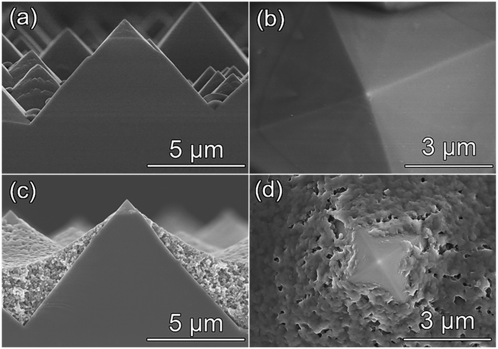 | ||
| Fig. 1 (a and b) Side and top view SEM images of pyramid Si spin coated with SOD polymer solution; (c and d) side and top view SEM images of pyramid Si spin coated with ADP aqueous solution. All samples were baked at 100 °C for 10 min. | ||
2.2 Uniform buried pn junctions for improved PEC performance
The PEC HER performance of pyramid pn+Si/Pt photocathodes would be largely affected by the distribution of phosphorous containing doping sources that were spin coated on pyramid p-Si substrates prior to annealing. There was no significant change in the morphology of Si substrates before and after annealing when use ADP aqueous solution as the phosphorous source (Fig. S2†) because ADP is completely decomposed into P2O5 and the generated phosphosilicate glass can be removed entirely with the subsequent HF etching (details in the ESI†).With the same Pt cocatalyst loading, the PEC HER performance of two electrodes doped using ADP aqueous solution (denoted as pn+Si(ADP)/Pt) and SOD polymer solution (denoted as pn+Si(SOD)/Pt) was compared under simulated AM 1.5G illumination (Fig. 2a), where the spin speed of ADP aqueous solution and SOD polymer solution was optimized (Fig. S6†) to ensure a fair comparison between the maximized PEC performances from the two methods. Before PEC measurements, N2 was continuously bubbled through the electrolyte for 10 min to remove dissolved O2 in order to reduce the possible unfavorable reaction on the Si photocathode, such as the oxygen reduction reaction. Compared with the pn+Si(SOD)/Pt photocathode, the uniform distribution of phosphorous containing doping sources on the pn+Si(ADP)/Pt photocathode results in an improved onset potential from 0.49 to 0.58 V vs. RHE and photocurrent density from 11.5 to 31.6 mA cm−2 at 0.3 V vs. RHE in a strongly acidic electrolyte (1 M HClO4, pH 0), reaching a fill factor of 55.4%. The ABPE of the pn+Si(ADP)/Pt photocathode achieved 10.6% at 0.37 V vs. RHE, which is 2.85 times that of the pn+Si(SOD)/Pt photocathode (3.72% at 0.21 V vs. RHE). The photovoltage (details in Fig. S7†) of the pn+Si(ADP)/Pt photocathode was measured to be 0.58 V, higher than that of the pn+Si(SOD)/Pt photocathode (0.49 V) (Fig. 2c), which is consistent with photocurrent density versus applied potential (J–V) curves. Correspondingly, the pn+Si(ADP)/Pt photocathode presents an improved incident photo-to-current conversion efficiency (IPCE) compared to the pn+Si(SOD)/Pt photocathode (Fig. 2d), indicating that the pn+Si(ADP)/Pt photocathode converts more incident photons to electrons than the pn+Si(SOD)/Pt photocathode.
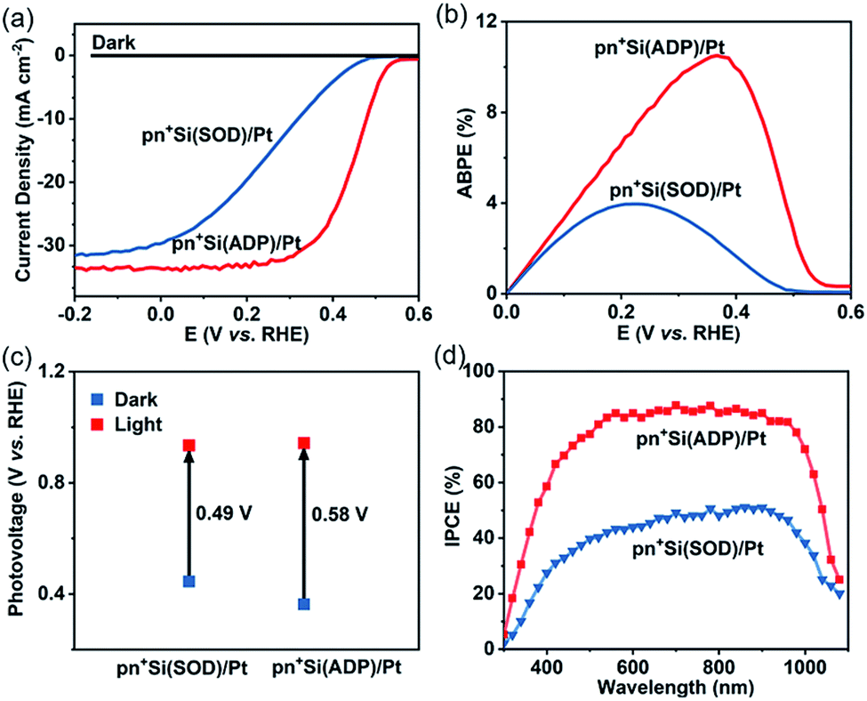 | ||
| Fig. 2 (a) J–V curves of pyramid pn+Si/Pt doped using ADP aqueous solution and SOD polymer solution under AM 1.5G illumination; (b) ABPE curves; (c) photovoltage under darkness and AM 1.5G illumination; (d) IPCE of pn+Si(ADP)/Pt and pn+Si(SOD)/Pt photocathodes as a function of wavelength at 0 V vs. RHE. 1 M HClO4 (pH 0) is used as the electrolyte in all measurements. | ||
Doping with a low viscosity dopant leads to different improvements in PEC performance between planar and pyramid p-Si substrates (Fig. S8†), suggesting that the low viscosity dopant exhibits great advantage for pyramid substrates. The slope of the J–V curve of the pyramid pn+Si(ADP)/Pt photocathode is much higher than that of the pyramid pn+Si(SOD)/Pt photocathode, while the slopes of J–V curves of planar pn+Si(ADP)/Pt and pn+Si(SOD)/Pt photocathodes show a slight difference, since both ADP aqueous solution and SOD polymer solution could provide sufficient doping source on planar p-Si substrates. For pyramid p-Si substrates, however, the highly viscous SOD polymer solution accumulates at the bottom, while the ADP aqueous solution can be uniformly dispersed on the surface of the pyramid structure, inducing different buried pn junctions. Moreover, planar pn+Si(SOD)/Pt and pn+Si(ADP)/Pt photocathodes presented much lower saturation photocurrent density than the pyramid pn+Si(ADP)/Pt photocathode because of their poor light absorption (Fig. S9†) and smaller junction interface. Additionally, the pyramid electrode exhibits a faster and more robust H2 bubble evolution with facile bubble detachment than the planar electrode (ESI Video†), which further reduces the light reflection and refraction.
The quality of the buried junction that is influenced by the distribution of phosphorous containing doping sources on the pyramid p-Si substrate could result in a notable difference of HER performance between pyramid samples doped using ADP aqueous solution and SOD polymer solution. Thus, it is assumed that the uniform distribution of phosphorous containing doping sources on the pyramid p-Si substrate may lead to a well-formed buried junction with even depth for the pn+Si(ADP)/Pt electrode, while the non-uniform distribution of phosphorous containing doping sources may lead to a low-quality buried junction for the pn+Si(SOD)/Pt electrode.
Given the fact that phosphorous polymers are accumulated at the bottom of pyramid p-Si substrates spin coated with SOD polymer solution (Fig. 1c and d), the junction depth at the top of the pyramid pn+Si(SOD) electrode is expected to be shallower than that at the bottom for the pn+Si(SOD) electrode, since the junction depth is mainly related to the surface phosphorus concentration at the same annealing temperature and duration.43 However, the uniform distribution of dopants on the pyramid p-Si substrate coated with ADP aqueous solution (Fig. 1a and b) is supposed to result in a more uniform junction along the surface of the pyramid pn+Si(ADP) electrode at fixed annealing temperature and time.
To confirm the assumption about the buried junction obtained by doping using ADP aqueous solution and SOD polymer solution, the combination and migration of photogenerated carriers in two electrodes were further explored. First, the uniformity of the junction depth of pn+Si(ADP) and pn+Si(SOD) electrodes was confirmed by photo-assisted deposition of Pt, where Pt4+ is easily reduced to Pt nanoparticles by photogenerated electrons that are separated by the buried junction. As for the pyramid pn+Si(SOD) electrode, the buried junction at the top of the pyramid may be too shallow to effectively separate photogenerated charges for Pt deposition. Thus, Pt nanoparticles on the pyramid pn+Si(SOD) electrode were mainly distributed at the bottom of the pyramid, and almost no Pt particles were observed at the top (Fig. 3b). For the pyramid pn+Si(ADP) electrode, in contrast, Pt nanoparticles could be uniformly deposited on the entire surface (Fig. 3a). The different distribution of these Pt nanoparticles indicates the difference of photo-electrons generated from the corresponding substrate, which validates the hypothesis that the distribution of dopants on the pyramid p-Si substrate significantly affects the uniformity of the buried pn junction. Furthermore, the pn+Si(SOD) electrode with an uneven buried pn junction exhibits a much stronger fluorescence signal than the pn+Si(ADP) electrode with a uniform buried pn junction, suggesting that more photogenerated charge carriers are recombined in the pn+Si(SOD) electrode, according to the steady-state photoluminescence spectroscopy (PL) emission spectra (Fig. 3c). Moreover, the PL intensity of the pn+Si(ADP) sample is further reduced upon the deposition of the 18 nm TiO2 protective layer, indicating the passivation effect of the TiO2 thin film. Upon doping pyramid p-Si using a low viscosity dopant, photogenerated carriers are separated by a uniform buried junction and photogenerated electrons migrate to the electrode surface efficiently.
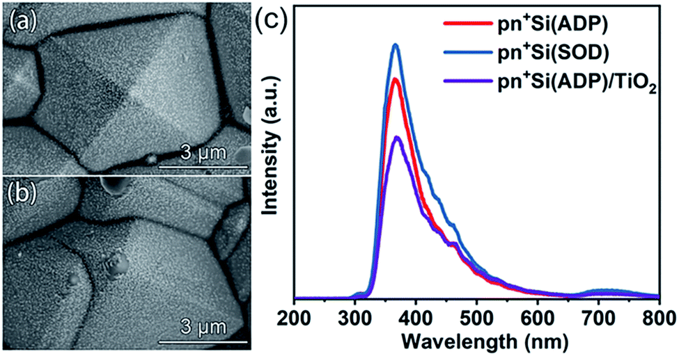 | ||
| Fig. 3 Top view SEM images of pyramid pn+Si/Pt (photo deposition) with (a) SOD and (b) ADP aqueous solution; (c) PL spectra (λex = 238 nm) of pyramid pn+Si photocathodes with different dopants and 18 nm TiO2 layers. | ||
The structures and energy band diagrams of the two types of buried junctions fabricated using ADP aqueous solution and SOD polymer solution are illustrated in the schematic diagram of the electrode, where the Pt cocatalyst and the band bending at the solid/liquid interface are neglected for clarity purpose (Fig. 4). For the pn+Si(ADP)44 electrode, the uniform buried junction from top to bottom of the pyramid Si substrate makes it possible for the whole surface to efficiently separate photogenerated carriers and transfer them to the surface for the hydrogen evolution reaction (Fig. 4a). For the pn+Si(SOD) electrode, however, the depth of the buried junction decreases gradually from the bottom to the top of the pyramid (Fig. 4b), where the pn junction at the top of the pyramid is too shallow, if not completely disappear, to offer enough band bending to separate photogenerated carriers, resulting in severe carrier recombination at the top of the pyramid and low hydrogen production efficiency upon illumination. Thus, the low viscosity dopant is well-suitable for doping pyramid substrates to form the uniform buried junction, which plays a critical role in improving the PEC HER performance of pyramid p-Si.
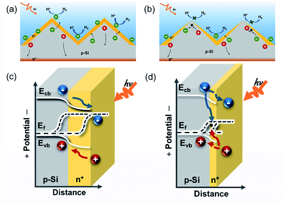 | ||
| Fig. 4 Schematic illustration of pn+Si doped using (a) ADP aqueous solution and (b) SOD polymer solution; energy band diagram at the (c) bottom and (d) top of pyramid Si in schematic illustration (b). | ||
Another key parameter for PEC water splitting is the stability of the electrode under operational conditions. Under the protection of the 18 nm ALD-grown TiO2 protective layer, the pn+Si(ADP)/TiO2/Pt electrode exhibited a reproducible stability of 250 h (details in the ESI, Fig. S10†), with a robust photocurrent density dropping by about 25% (Fig. 5). The surface morphology of the pn+Si(ADP)/TiO2/Pt electrode changes after the 250 h stability test, where the electrode shows a membranous surface while the original surface was uniformly decorated with Pt particles (Fig. S11†). However, there is no decrease in the slope and onset potential of the J–V curve of the pn+Si(ADP)/TiO2/Pt electrode after the 250 h stability test (Fig. S12†), indicating that the Pt cocatalyst maintains sufficient activity after the stability test. Therefore, the reduction of incident light absorbed by the photoelectrode, which could be caused by the accumulation of the electrolyte from the reference electrode (RE) transferred slowly through the porous ceramic plug of the RE over the 250 h stability test19,45,46 (details in the ESI†), is probably the reason of the decrease of photocurrent density. In addition, a control experiment of the pn+Si(ADP)/Pt photocathode without a TiO2 protective layer was performed in the same electrolyte, which showed much quicker decline of photocurrent with a significant decrease of the fill factor (from 51.2% to 2.6%) (Fig. S13†). Thus, the excellent PEC performance of the pn+Si(ADP)/TiO2/Pt photocathode after the 250 h stability test indicates that the 18 nm TiO2 film is capable of protecting Si against corrosion in a relatively long duration. Compared with previously reported pn+Si photocathodes doped using other phosphorous sources, pn+Si(ADP)/TiO2/Pt presents one of the best performances in terms of onset potential, ABPE, and long term stability (Fig. S14 and Table S3†).
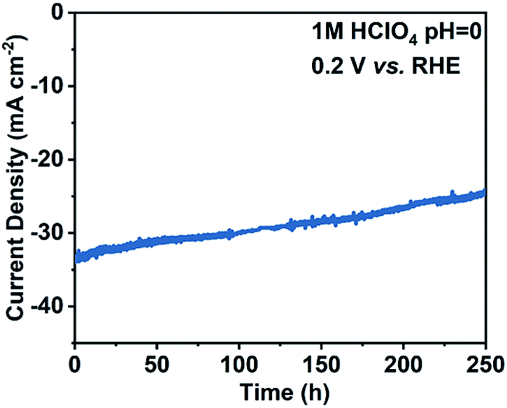 | ||
| Fig. 5 Stability test of the pn+Si(ADP)/TiO2/Pt photocathode at 0.2 V vs. RHE measured in 1 M HClO4 electrolyte under simulated AM 1.5G illumination. | ||
2.3 Unassisted water splitting
An unassisted water splitting system driven only by sunlight is demonstrated (inset of Fig. 6b), where a pn+Si(ADP)/TiO2/Pt photocathode in 1 M HClO4 (pH 0) was connected with a BiVO4/CoOx photoanode in 1 M potassium borate (pH 9), separated with a proton exchange membrane and tested under simulated AM 1.5G illumination. The J–V characteristics of the BiVO4 photoanode and pn+Si (behind BiVO4) photocathode were obtained in the three-electrode configuration respectively, where a theoretical photocurrent density of ∼1.9 mA cm−2 is predicted based on the intersection of the two J–V curves, corresponding to a solar-to-hydrogen (STH) conversion efficiency of 2.34% (Fig. 6a). In the two-electrode tandem configuration, the Si photocathode was connected with the BiVO4 photoanode in series without external bias. Meanwhile, the Si photocathode was placed behind the BiVO4 photoanode to absorb the photons with energy less than the bandgap of the BiVO4. Finally, an actual photocurrent density of 1.7 mA cm−2 was obtained with the unbiased two-electrode configuration (Fig. 6b), smaller than the estimated value of ∼1.9 mA cm−2, which may result from polarization losses.47,48 Assuming a faradaic efficiency of 100% according to the stable photocurrent during the test duration, this photocurrent corresponds to an STH conversion efficiency of ∼2.09%. This tandem configuration ultimately exhibits a high stability of continuous 1.5 h with 11% photocurrent drop under AM 1.5G illumination.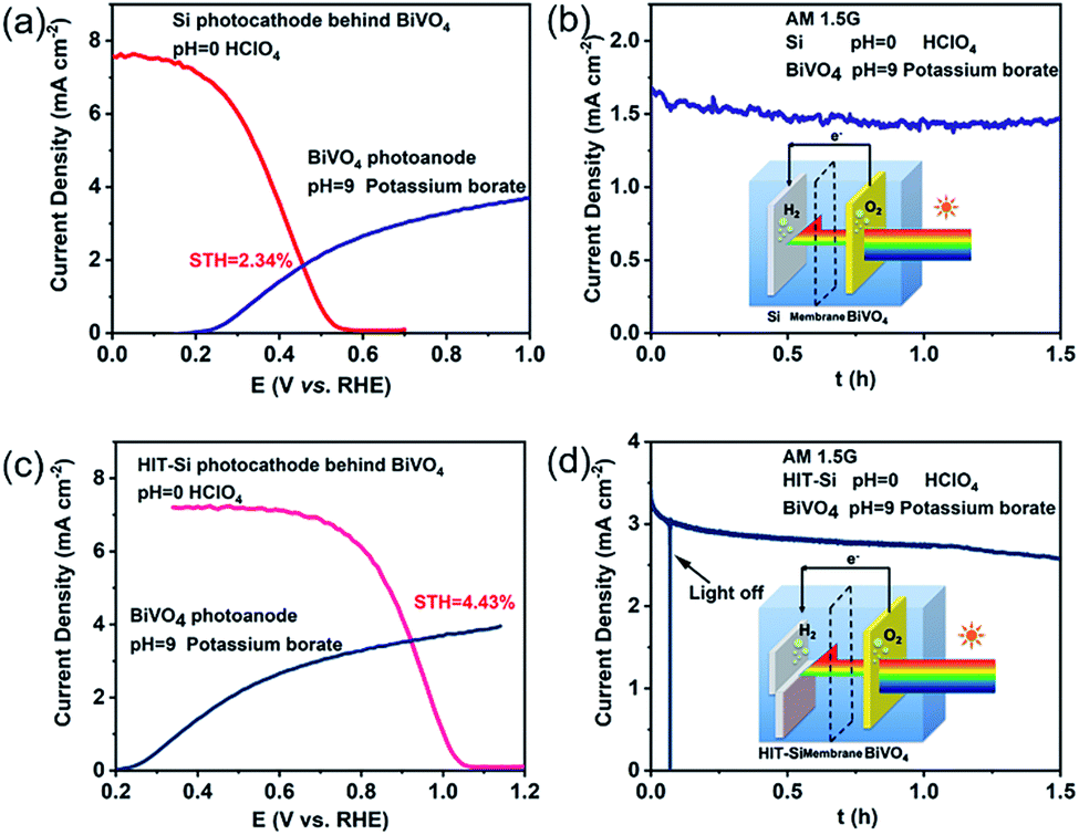 | ||
| Fig. 6 (a) J–V curves of the pn+Si(ADP)/TiO2/Pt photocathode (behind BiVO4) and BiVO4/CoOx photoanode under AM 1.5G illumination using a three-electrode configuration, respectively. (b) Stability test of the two-electrode cell under AM 1.5G illumination in 1 M HClO4 (pH 0) and 1 M potassium borate buffer solution (pH 9), respectively, separated with the proton exchange membrane. (c) J–V curves of the HIT-pn+Si(ADP)/TiO2/Pt photocathode (behind BiVO4) and BiVO4/CoOx photoanode under AM 1.5G illumination using a three-electrode configuration, respectively. (d) Stability test of the two-electrode cell under AM 1.5G illumination in 1 M HClO4 (pH 0) and 1 M potassium borate buffer solution (pH 9), respectively, separated with the proton exchange membrane. Illustrations show schematic diagrams of two-electrode devices. | ||
To overcome the inherent low photovoltage of the single Si photocathode and further increase the STH conversion efficiency, a heterojunction with intrinsic thin-layer (HIT) solar cell (Fig. S15†) is connected to the pn+Si(ADP)/TiO2/Pt electrode in series (denoted as HIT-pn+Si(ADP)/TiO2/Pt photocathode), which forms a new photocathode (inset of Fig. 6d, details in Fig. S16†). The onset potential of the HIT-pn+Si(ADP)/TiO2/Pt photocathode increases to ∼1.08 V vs. RHE, while the theoretical photocurrent density becomes ∼3.6 mA cm−2, yielding an STH conversion efficiency of 4.43% (Fig. 6c). The actual STH conversion efficiency is higher than 4.1% in the two-electrode configuration (Fig. 6d), while the decline of performance in the 1.5 h stability test is possibly due to the insufficient mass transfer when the photocathode and photoanode are working in a PEC cell separated with the membrane,49 which could be more significant with a larger current density when the HIT solar cell is connected with the pn+Si photoelectrode.
3. Conclusions
In summary, we have successfully fabricated an efficient pyramid pn+Si/Pt electrode with uniform buried junctions using a low viscosity dopant. The ADP aqueous solution with low viscosity as the phosphorous source is more suitable to dope pyramid p-Si substrates compared with SOD polymer solution that is of high viscosity and much safer compared to the toxic POCl3 and PH3 used in industry. Photogenerated electrons efficiently migrate to the entire surface of the pyramid pn+Si(ADP) electrode for the reduction reaction, while almost no electrons are present at the top of the pyramid pn+Si(SOD) electrode owing to local severe recombination, which is evidenced by the different distribution of deposited Pt nanoparticles on pyramid pn+Si(ADP) and pn+Si(SOD) electrodes. The pyramid pn+Si(ADP)/TiO2/Pt photocathode with highly uniform buried junctions achieves an ABPE of 10.6% at 0.37 V vs. RHE and more than 10 days of stability at 0.2 V vs. RHE bias in strong acid electrolyte under AM 1.5G irradiation. Furthermore, pn+Si(ADP)/TiO2/Pt–BiVO4/CoOx and HIT-pn+Si(ADP)/TiO2/Pt–BiVO4/CoOx tandem cells achieve STH conversion efficiencies of 2.09% and 4.1% without external bias, respectively. This study offers a safe, low-cost and efficient method to dope pyramid Si for solar hydrogen generation. Additionally, it is possible to adopt this facile doping strategy for other non-planar Si structures with uneven surfaces, such as Si microwires, by further optimization of spin speed.Conflicts of interest
There are no conflicts to declare.Acknowledgements
We acknowledge the National Key R&D Program of China (2016YFB0600901), the National Natural Science Foundation of China (21525626, U1463205, U1662111, 21722608, and 51861125104), the Natural Science Foundation of Tianjin City (18JCJQJC47500), and the Program of Introducing Talents of Discipline to Universities (B06006) for financial support.Notes and references
- N. S. Lewis, Nature, 2001, 414, 589–590 CrossRef CAS PubMed.
- J. A. Turner, Science, 2004, 305, 972–974 CrossRef CAS PubMed.
- N. S. Lewis, Science, 2016, 351, 353 CrossRef CAS.
- R. C. Armstrong, C. Wolfram, K. P. de Jong, R. Gross, N. S. Lewis, B. Boardman, A. J. Ragauskas, K. Ehrhardt-Martinez, G. Crabtree and M. V. Ramana, Nat. Energy, 2016, 1, 15020 CrossRef.
- H. Kumagai, T. Minegishi, N. Sato, T. Yamada, J. Kubota and K. Domen, J. Mater. Chem. A, 2015, 3, 8300–8307 RSC.
- M. X. Chen, Y. Liu, C. C. Li, A. Li, X. X. Chang, W. Liu, Y. Sun, T. Wang and J. L. Gong, Energy Environ. Sci., 2018, 11, 2025–2034 RSC.
- H. Kobayashi, N. Sato, M. Orita, Y. Kuang, H. Kaneko, T. Minegishi, T. Yamada and K. Domen, Energy Environ. Sci., 2018, 11, 3003–3009 RSC.
- M. H. Lee, K. Takei, J. Zhang, R. Kapadia, M. Zheng, Y. Z. Chen, J. Nah, T. S. Matthews, Y. L. Chueh, J. W. Ager and A. Javey, Angew. Chem., Int. Ed., 2012, 51, 10760–10764 CrossRef CAS.
- A. Paracchino, V. Laporte, K. Sivula, M. Gratzel and E. Thimsen, Nat. Mater., 2011, 10, 456–461 CrossRef CAS.
- T. Wang, Y. Wei, X. Chang, C. Li, A. Li, S. Liu, J. Zhang and J. Gong, Appl. Catal., B, 2018, 226, 31–37 CrossRef CAS.
- J. Azevedo, S. D. Tilley, M. Schreier, M. Stefik, C. Sousa, J. P. Araújo, A. Mendes, M. Grätzel and M. T. Mayer, Nano Energy, 2016, 24, 10–16 CrossRef CAS.
- J. Li and N. Wu, Catal. Sci. Technol., 2015, 5, 1360–1384 RSC.
- K. Sun, S. H. Shen, Y. Q. Liang, P. E. Burrows, S. S. Mao and D. L. Wang, Chem. Rev., 2014, 114, 8662–8719 CrossRef CAS.
- T. Wang and J. Gong, Angew. Chem., Int. Ed., 2015, 54, 10718–10732 CrossRef CAS.
- C. J. Chen, K. C. Yang, C. W. Liu, Y. R. Lu, C. L. Dong, D. H. Wei, S. F. Hu and R. S. Liu, Nano Energy, 2017, 32, 422–432 CrossRef CAS.
- S. W. Boettcher, J. M. Spurgeon, M. C. Putnam, E. L. Warren, D. B. Turner-Evans, M. D. Kelzenberg, J. R. Maiolo, H. A. Atwater and N. S. Lewis, Science, 2010, 327, 185–187 CrossRef CAS.
- H. Seidel, L. Csepregi, L. Csepregi and H. BaumgSrtel, J. Electrochem. Soc., 1990, 137, 3612–3626 CrossRef CAS.
- M. G. Kast, L. J. Enman, N. J. Gurnon, A. Nadarajah and S. W. Boettcher, ACS Appl. Mater. Interfaces, 2014, 6, 22830–22837 CrossRef CAS.
- R. Fan, W. Dong, L. Fang, F. Zheng and M. Shen, J. Mater. Chem. A, 2017, 5, 18744–18751 RSC.
- Z. Yin, R. Fan, G. Huang and M. Shen, Chem. Commun., 2018, 54, 543–546 RSC.
- B. M. Kayes, M. A. Filler, M. C. Putnam, M. D. Kelzenberg, N. S. Lewis and H. A. Atwater, Appl. Phys. Lett., 2007, 91, 103110 CrossRef.
- J. M. Yan, S. L. Wu, X. F. Zhai, X. Gao and X. F. Li, RSC Adv., 2016, 6, 87486–87492 RSC.
- S. Gopalakrishnan and K. Jeganathan, Int. J. Hydrogen Energy, 2017, 42, 22671–22676 CrossRef CAS.
- X.-Q. Bao and L. Liu, J. Power Sources, 2014, 268, 677–682 CrossRef CAS.
- S. Chandrasekaran, T. Nann and N. H. Voelcker, Nano Energy, 2015, 17, 308–322 CrossRef CAS.
- S. W. Boettcher, E. L. Warren, M. C. Putnam, E. A. Santori, D. Turner-Evans, M. D. Kelzenberg, M. G. Walter, J. R. McKone, B. S. Brunschwig, H. A. Atwater and N. S. Lewis, J. Am. Chem. Soc., 2011, 133, 1216–1219 CrossRef CAS.
- D. V. Esposito, I. Levin, T. P. Moffat and A. A. Talin, Nat. Mater., 2013, 12, 562–568 CrossRef CAS PubMed.
- L. Ji, M. D. McDaniel, S. Wang, A. B. Posadas, X. Li, H. Huang, J. C. Lee, A. A. Demkov, A. J. Bard, J. G. Ekerdt and E. T. Yu, Nat. Nanotechnol., 2014, 10, 84–90 CrossRef.
- T. Zhu and M. N. Chong, Nano Energy, 2015, 12, 347–373 CrossRef CAS.
- K. Sun, K. Madsen, P. Andersen, W. Bao, Z. Sun and D. Wang, Nanotechnology, 2012, 23, 194013 CrossRef.
- S. S. Liu, Z. B. Luo, L. L. Li, H. M. Li, M. X. Chen, T. Wang and J. L. Gong, Nano Energy, 2018, 53, 125–129 CrossRef CAS.
- H. P. Wang, K. Sun, S. Y. Noh, A. Kargar, M. L. Tsai, M. Y. Huang, D. Wang and J. H. He, Nano Lett., 2015, 15, 2817–2824 CrossRef CAS.
- Y. Tang, C. Zhou, W. Wang, Y. Zhao, S. Zhou, J. Fei and H. Cao, Sol. Energy, 2013, 95, 265–270 CrossRef CAS.
- B. Seger, A. B. Laursen, P. C. K. Vesborg, T. Pedersen, O. Hansen, S. Dahl and I. Chorkendorff, Angew. Chem., Int. Ed., 2012, 51, 9128–9131 CrossRef CAS.
- A. Yadav, G. Singh, R. Nekovei and R. Jeyakumar, Renewable Energy, 2015, 80, 80–84 CrossRef CAS.
- K. Sopian, S. L. Cheow and S. H. Zaidi, 4th International Conference on the Advancement of Materials and Nanotechnology, 2017, vol. 1877, p. 020004 Search PubMed.
- D. Mathiota, A. Lachiqa, A. Slaouia, S. NoeÈla, J. C. Mullera and C. Duboisb, Mater. Sci. Semicond. Process., 1998, 231–236 CrossRef.
- M. Edwards, J. Bocking, J. E. Cotter and N. Bennett, Prog. Photovoltaics, 2008, 16, 31–45 CAS.
- M. L. Hoarfrost, K. Takei, V. Ho, A. Heitsch, P. Trefonas, A. Javey and R. A. Segalman, J. Phys. Chem. Lett., 2013, 4, 3741–3746 CrossRef CAS.
- J. O'Connell, S. Biswas, R. Duffy and J. D. Holmes, Nanotechnology, 2016, 27, 342002 CrossRef PubMed.
- Y. Su, C. Liu, S. Brittman, J. Tang, A. Fu, N. Kornienko, Q. Kong and P. Yang, Nat. Nanotechnol., 2016, 11, 609–612 CrossRef CAS PubMed.
- W. Vijselaar, R. M. Tiggelaar, H. Gardeniers and J. Huskens, ACS Energy Lett., 2018, 1086–1092 CrossRef CAS PubMed.
- E. Tannenbaum, Solid-State Electron., 1961, 2, 123–132 CrossRef.
- W. Zagozdzon-Wosik, P. B. Grabiec and G. Lux, J. Appl. Phys., 1994, 75, 337–344 CrossRef CAS.
- M. P. Mousavi and P. Buhlmann, Anal. Chem., 2013, 85, 8895–8901 CrossRef CAS.
- A. Yakushenko, D. Mayer, J. Buitenhuis, A. Offenhausser and B. Wolfrum, Lab Chip, 2014, 14, 602–607 RSC.
- K. Zhang, M. Ma, P. Li, D. H. Wang and J. H. Park, Adv. Energy Mater., 2016, 6, 1600602 CrossRef.
- J. Jin, K. Walczak, M. R. Singh, C. Karp, N. S. Lewis and C. Xiang, Energy Environ. Sci., 2014, 7, 3371–3380 RSC.
- M. R. Singh, K. Papadantonakis, C. Xiang and N. S. Lewis, Energy Environ. Sci., 2015, 8, 2760–2767 RSC.
Footnote |
| † Electronic supplementary information (ESI) available. See DOI: 10.1039/c9ta09652c |
| This journal is © The Royal Society of Chemistry 2020 |