
A review of aspects of additive engineering in perovskite solar cells
Apurba
Mahapatra†
 a,
Daniel
Prochowicz†
b,
Mohammad Mahdi
Tavakoli
*c,
Suverna
Trivedi
d,
Pawan
Kumar
a and
Pankaj
Yadav
*e
a,
Daniel
Prochowicz†
b,
Mohammad Mahdi
Tavakoli
*c,
Suverna
Trivedi
d,
Pawan
Kumar
a and
Pankaj
Yadav
*e
aDepartment of Physics & Astronomy, National Institute of Technology Rourkela, 769008, India
bInstitute of Physical Chemistry, Polish Academy of Sciences, Kasprzaka 44/52, 01-224 Warsaw, Poland
cDepartment of Electrical Engineering and Computer Science, Massachusetts Institute of Technology, Cambridge, MA 02139, USA. E-mail: mtavakol@mit.edu
dDepartment of Chemical Engineering, School of Technology, Pandit Deendayal Petroleum University, Gandhinagar-382 007, Gujarat, India
eDepartment of Solar Energy, School of Technology, Pandit Deendayal Petroleum University, Gandhinagar-382 007, Gujarat, India. E-mail: pankaj.yadav@sse.pdpu.ac.in; pankajphd11@gmail.com
First published on 5th December 2019
Abstract
Solar energy is a clean source of energy that can help fulfill the increasing global energy demand. Among light harvesting devices, perovskite solar cells (PSCs) have been a focus of interest among next-generation photovoltaic (PV) technologies due to their incredible conversion efficiency (certified PCE of 25.2%) along with their lower cost and ease of fabrication. However, the presence of many transport barriers and defect trap states at the interfaces and grain boundaries has negative effects on PSCs; it decreases their efficiency and stability and increases the hysteresis effect. Further controlling the morphology, grain boundary, grain size, charge recombination and density of defect states in the perovskite layer is necessary to enhance its photovoltaic performance and stability. In this review, we summarize the intensive research efforts in aspects of additive engineering in PSCs, including physical and chemical passivation, and the use of a wide variety of organic and inorganic additives to address these issues. Here, we mainly focus on passivation techniques in the perovskite active layer and their effects on the PV performance and stability of PSCs; the grain boundaries and surface defects in the perovskite layer play major roles in the recombination, carrier lifetime and charge transfer of PSCs.
1. Introduction
The global energy demand is increasing due to population growth and industrial development. This demand is mainly addressed by fossil fuels such as coal and oils, which will be depleted in the near future. Therefore, it is important to find long-lasting, clean and renewable alternative energy sources to fossil fuels. Solar energy is a clean energy source that can fulfill the global energy demand and can be directly converted into electricity using photovoltaic (PV) devices. Perovskite solar cells (PSCs) have been a center of interest among next-generation photovoltaic technologies due to their incredible power conversion efficiency (PCE) along with their lower cost and ease of fabrication.1 The first photovoltaic device based on a lead halide perovskite material with a PCE of 2.2.% was reported by Miyasaka and co-workers using CH3NH3PbBr3.2 By replacing bromine with iodine in CH3NH3PbBr3, the PCE was slightly increased to 3.8%.3 After that, in 2012, Kim et al. successfully fabricated the first solid state perovskite solar cell with a PCE of 9.7% using spiro-MeOTAD as a hole-transporting layer.4 Remarkably, in just the next few years, PSCs reached certified power conversion efficiencies (PCE) of over 23%; this was realized in 2017 by engineering the perovskite composition and thin film deposition method.5,6 More recently, the certified PCE of PSCs increased even further to 25.2%, as can be found in the NREL PV chart.7It has been theoretically demonstrated that a good perovskite absorber shows excellent electronic dimensionality for PV applications; this is mostly fulfilled by the 3D lead halide perovskites.8 These semiconductor materials exhibit unique physicochemical properties, such as low band gaps, high light extinction coefficients, long charge carrier diffusion lengths, long charge carrier lifetimes and high charge carrier mobilities.9–11 Despite the success of 3D perovskite-based devices in enhancing the efficiency of PSCs and their low fabrication cost, these devices still face several critical challenges, including lead toxicity and low long-term stability.12 In the context of toxicity, there has been growing research interest in developing alternative lead-free perovskites with low toxicity and high stability.13 Some lead-free elements, e.g., tin (Sn), germanium (Ge), antimony (Sb) and bismuth (Bi), exhibit similar ionic radii, electron configurations and semiconducting characteristics; they have been proposed as potential candidates to address lead toxicity, but the resulting devices yielded lower PCE values than those reported with lead halide perovskites.14 The instability of 3D lead halide perovskites to moisture, light, and heat is another issue that must be addressed.15 To overcome this issue, numerous efforts have been made to enhance the stability of devices, including compositional engineering,16,17 interface passivation,18,19 encapsulation techniques,20 and device structure engineering.21–23 Among these, passivation techniques appear to be efficient approaches for the fabrication of highly efficient and stable PSCs;24,25 some of these aspects have been addressed in recent reviews.26–28
In general, these materials are protected from corrosion by a process called passivation. According to the International Union of Pure and Applied Chemistry (IUPAC), when materials become “passive”, they are also less affected by the environment.29 In the process of passivation, a microcoating of protective material is produced by a chemical reaction with the base material. Passivation in PSCs mainly refers to either physical or chemical passivation. In the process of physical passivation, an additional coating on the functional layer isolates it from the external environment and improves the stability of the device. In the case of chemical passivation, the charge transfer is optimized between various interfaces of PSCs by decreasing the defect trap states of the materials.30–34 A typical device mainly contains five layers, including a transparent conductive oxide (TCO), an electron transport layer (ETL), a light-absorbing perovskite material, a hole transporting layer (HTL) and a metal electrode (Fig. 1). Different passivation techniques are being used to overcome the main barriers to the further commercialization of PSCs.
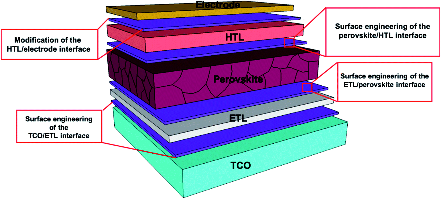 | ||
| Fig. 1 Normal structure of a perovskite solar cell consisting of a transparent conductive oxide (TCO), electron transport layer (ETL), light-absorbing perovskite material, hole transporting layer (HTL) and metal electrode. | ||
In this review, we summarize the recent research progress on the effects of applying passivation agents in different layers in the PSC structure on the overall stability and performance of the devices; we mainly concentrate on passivation techniques in the perovskite active layer. Moreover, the challenges and the scope of passivation techniques for obtaining efficient PSCs are presented.
2. Surface engineering of the TCO/ETL interface
The interlayer between the TCO and ETL for the purpose of surface engineering is required to be significantly transparent and conductive and to have desirable optoelectronic properties. In this context, graphene possesses a high charge carrier mobility (106 cm2 V−1 s−1) and a transmittance of 98%; the entire visible light spectrum shows beneficial effects on electron transport.35,36 Wang et al. demonstrated that the deposition of a nanocomposite consisting of graphene nanoflakes and anatase-TiO2 nanoparticles on an FTO layer significantly improved the performance of solar cells (Fig. 2a).37 The enhancement of the photovoltaic parameters was attributed to the better conductivity and favorable electron transport of the graphene layer, as demonstrated by the energy level diagram shown in Fig. 2b. Moreover, the applied low temperature fabrication process of the graphene–TiO2 nanocomposite (∼150 °C) decreases the series resistance and recombination losses at the FTO/ETL interface.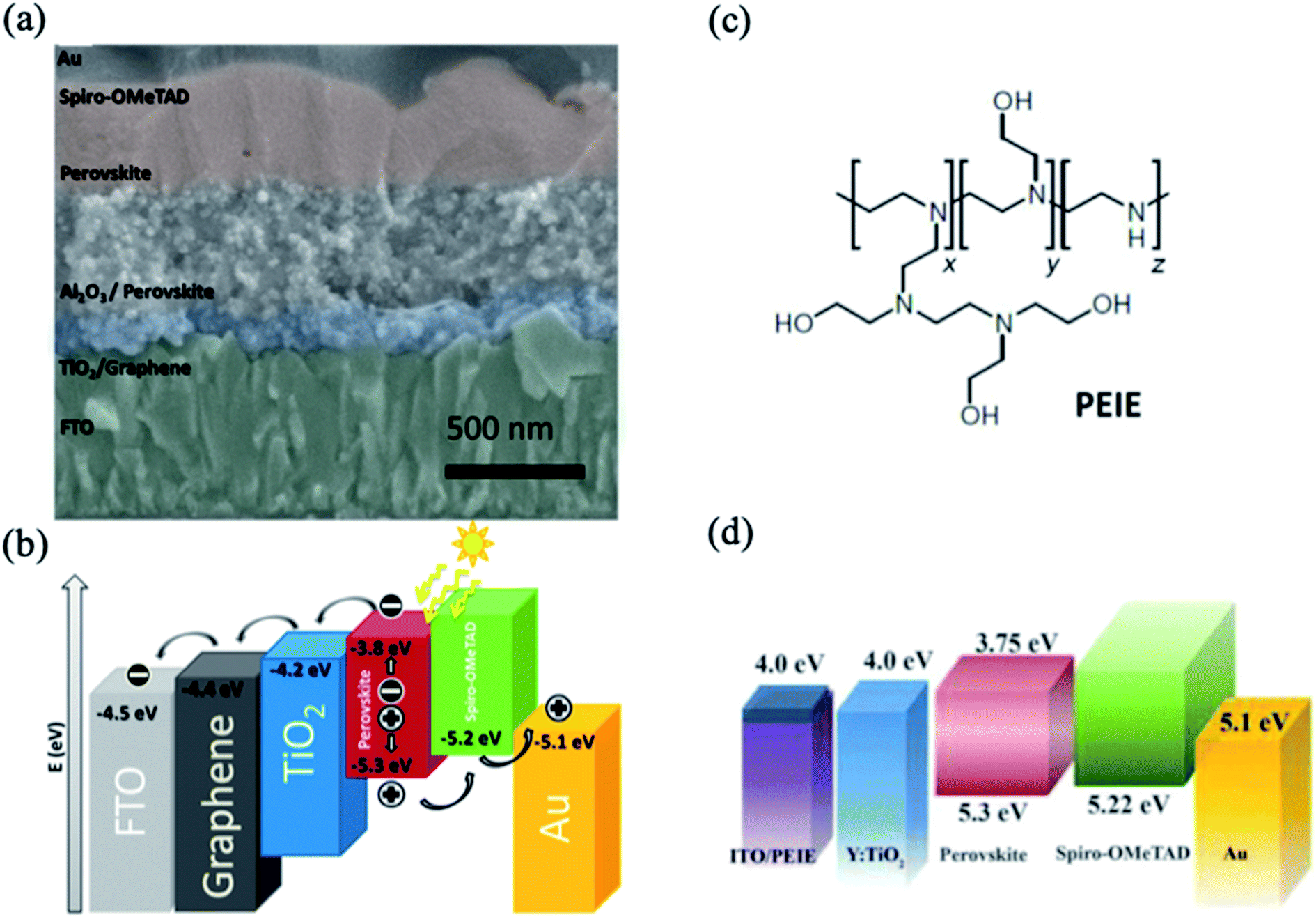 | ||
| Fig. 2 (a) Cross-sectional SEM image of a planar device employing graphene–TiO2 nanocomposite on FTO. (b) Energy level diagram of a PSC with an interfacial graphene layer. Reprinted with permission from ref. 37. Copyright 2014 American Chemical Society. (c) Chemical structure of polyethyleneimine ethoxylate. (d) Energy level diagram of a PSC with PEIE-coated ITO substrate. Reprinted with permission from ref. 38. Copyright 2012 American Association for the Advancement of Science. | ||
Another approach to modify the interlayer between TCO and ETL is to decrease the work function of the electrode materials. A nonconjugated polymer, ethoxylated polyethylenimine (PEIE), has emerged as an efficient surface modifier of various conductive metal oxides, including ITO and FTO (Fig. 2c).38 The work function of the electrode is changed due to slight electron transfer from the amine-containing molecules to the electrode surface. Zhou et al. demonstrated the use of a PEIE modifier to decrease the work function of ITO in PSCs, which enhances the charge transfer between the ETL and ITO layers.39 Specifically, the energy level of the PEIE-coated ITO was found to be close to the conduction-band position of the ETL layer, which allows efficient transport of photogenerated carriers without excessive interface recombination (Fig. 2d).
3. Surface engineering of the ETL/perovskite interface
The type of material selected as the ETL in a PSC can tune the photovoltaic performance of the device.40 In general, the ETL plays an important role in the extraction and transportation of photogenerated carriers in PSCs. Moreover, the thin layer of ETL eliminates electrical shunts between the transparent electrode and perovskite layers. Currently, titanium dioxide (TiO2) is most commonly used as an ETL in planar heterojunction solar cells due to its suitable band alignment with the perovskite layer and good transparency to visible light. However, in the presence of UV light, the TiO2 ETL behaves as an excellent photocatalyst, which decreases the stability of the PSC. In addition, TiO2 contains a high surface defect density and intrinsically low mobility, which limits the photovoltaic performance of devices.41,42 These issues can be resolved by coating the original TiO2 surface with another ultrathin TiO2 film using atomic layer deposition (ALD)43 or chemical bath deposition (CBD).44 Recently, various modifications of the TiO2 surface have been proposed, such as (1) doping treatment with metal or non-metal ions or (2) passivation using a fullerene self-assembled monolayer, (3) graphene-based material, or (4) organic or inorganic self-assembled monolayer; this will be exemplified in this chapter.3.1. Surface treatment with metal or non-metal ions
Doping with metal or non-metal elements has been widely attempted to controllably tune the properties of TiO2, which subsequently leads to enhanced photovoltaic performance. It was demonstrated that doping of TiO2 improves the conduction band edge and decreases the charge recombination process at the interface. Several metal and non-metal ions, e.g. Y3+,45 Li,46 Ru2+,47 Mg2+,48 Nd3+,49 La3+,50 Er3+,51 and Cl−,52 have been reported to have positive effects on the overall performance of TiO2-based PSCs. For example, Xu et al.47 used Ru-doped TiO2 as an ETL to improve the conductivity of the ETL and enhance the photovoltaic performance of planar heterojunction PSCs. The Ru–TiO2 layer improves the charge injection and transport properties due to its good energy band match with the perovskite layer, which decreases the energy loss of the electrons during transportation (Fig. 3a). Consequently, the devices with Ru-doped TiO2 ETLs exhibit superior PCE (up to 15.7%) compared to devices using a pristine TiO2 layer (13.42%). In other relevant work, a Li-doped TiO2 ETL was demonstrated to exhibit superior electronic properties by passivating electronic defect states acting as nonradioactive recombination centers. Doping with a proper concentration of ETL enhances the photovoltaic performance of the device, which is attributed to the decreased selective contact resistance and the increased charge recombination resistance at the ETL/perovskite interface.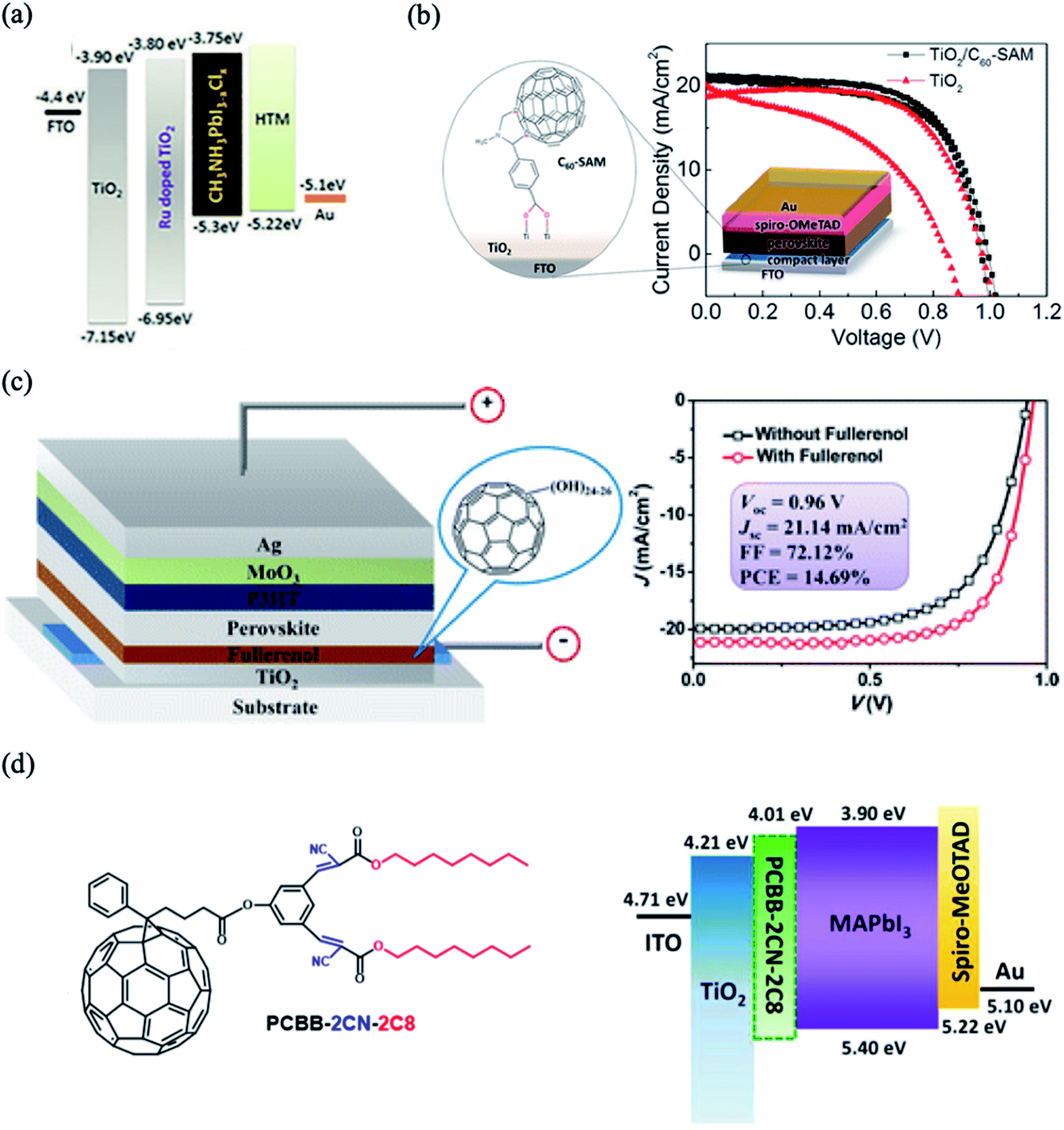 | ||
| Fig. 3 (a) Energy level diagram of the device with Ru-doped TiO2. Reprinted with permission from ref. 47. Copyright 2018 Royal Chemical Society. (b) Schematic structure of C60-substituted benzoic acid and comparison of current–voltage curves before and after TiO2 modification. Reprinted with permission from ref. 56. Copyright 2014 American Chemical Society. (c) Device configuration of PSCs incorporated with fullerenol as the ETL and comparison of current–voltage curves before and after TiO2 modification. Reprinted with permission from ref. 53. Copyright 2016 American Chemical Society. (d) Chemical structure of PCBB-2CN-2C8 and energy level diagram of the device with an interfacial layer of PCBB-2CN-2C8 between the TiO2 and MAPbI3. Reprinted with permission from ref. 25. Copyright 2017 Wiley-VCH. | ||
3.2. Surface passivation using a fullerene self-assembled monolayer
The charge transfer between the perovskite layer and the ETL layer can be improved using fullerene C60 and its derivatives, which enhance both the absorption and the electron injection. Fullerene self-assembled monolayers (C60SAMs) were successfully introduced on the TiO2 surface to decrease the capacitance and trap states of the TiO2. The conducting properties of the C60SAM-doped ETL can be enhanced by grafting different functional groups onto the fullerene cage, e.g. hydroxyl,53 ether,54 carboxyl,55,56 ester57 or amino58,59 groups. For example, inserting a C60-substituted benzoic acid self-assembled monolayer between the compact TiO2/perovskite interface improves the charge separation and photovoltaic performance. The fullerene-modified devices yielded a maximum PCE of 17.3% with significantly decreased hysteresis (Fig. 3b). The carboxylate anchoring groups grafted on fullerene passivate the defective trap states in the TiO2 by chemically binding to the TiO2 surface hydroxyl groups, which decreases the nonradiative recombination at this interface. In a similar manner, fullerenol hydroxylated C60 proved to be a promising interfacial material for improving the performance and stability of PSCs (Fig. 3c).53 This modification facilitates the charge transportation and decreases the interfacial resistance at the ETL/perovskite interface. Li et al. inserted a triblock fullerene derivative, [6,6]-phenyl-C61-butyric acid-dioctyl-3,3′-(5-hydroxy-1,3-phenylene)-bis(2-cyanoacrylate) ester (PCBB-2CN-2C8), as a cathode modification monolayer on TiO2; it possesses dioctyloxy chains and cyano-groups, which minimize its solubility in polar solvents (Fig. 3d).60 The modification of TiO2 with PCBB-2CN-2C8 decreases the trap states of TiO2 by adsorption of electron-withdrawing cyano-groups and C60 carbon balls on the oxygen vacancies and changes the energy band alignment; this improves the electron extraction from perovskite to the ETL. This surface passivation process significantly enhances the values of Voc from 0.99 to 1.06 V and FF from 72.2% to 79.1%, leading to improvements in the PCE of up to 20.7%.3.3. Surface passivation using graphene-based materials
Recently, research groups have focused on the role of graphene quantum dots (GQDs) in the interfacial engineering of PSCs due to their high charge carrier mobility and high transmittance in the entire visible light spectrum, which are attractive for photovoltaic applications.61–64 Inserting an ultrathin layer of GQDs between the perovskite and TiO2 ETL facilitates electron transfer, leading to significantly enhanced photocurrent and efficiency of the corresponding solar cells.65 The GQDs act as a superfast electron tunnel that strongly quenches the PL of the perovskite absorber and decreases the electron extraction time from 280 to 90 ps (Fig. 4a). In another relevant study, Tavakoli et al. introduced monolayer graphene at the interface of the ZnO ETL and perovskite absorber, which enhanced the carrier extraction properties and photovoltaic performance up to 19.8%.66 Importantly, the presence of graphene at the ETL/perovskite interface protects the perovskite film from decomposition at elevated temperatures and enhances the overall stability of the device. In addition to the above work, the instability issue of CH3NH3PbI3 on ZnO nanoparticles was resolved by the synthesis of a reduced graphene oxide (rGO)/ZnO nanocomposite layer as an ETL.67 Recently, the combination of GQDs and SnO2 in an ETL emerged as an effective strategy for enhancing the electronic properties and performance of flexible PSCs.68 The optimized GQDs/SnO2 ETL exhibits higher electron mobility, better film coverage and better energy level alignment matching compared to the pristine SnO2 ETL, leading to enhanced charge transfer and suppressed charge recombination (Fig. 4b). As a result, the optimized device yielded PCEs of 19.6% for the rigid substrate and 17.7% for the flexible substrate.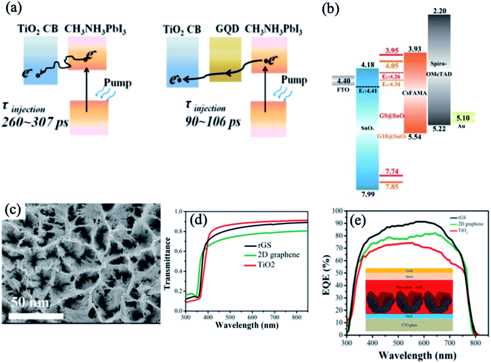 | ||
| Fig. 4 (a) Schematics of electron generation and extraction at TiO2/perovskite and GQD/TiO2/GQD/perovskite interfaces. Reprinted with permission from ref. 65. Copyright 2014 American Chemical Society. (b) Schematic of energy levels based on an FTO/SnO2/graphene/CsFAMA-perovskite/spiro-OMeTAD/Au device. Reprinted with permission from ref. 68. Copyright 2019 Royal Chemical Society. (c) Top-view SEM image of the rGS structure. (d) Transmittance spectra of the rGS, 2D graphene, and TiO2 films. (e) EQE spectra of the rGS, 2D graphene, and TiO2-based PSCs. Reprinted with permission from ref. 69. Copyright 2016 American Chemical Society. | ||
Reduced-graphene scaffold (rGS) is a type of three-dimensional (3D) graphene consisting of a porous structure with a high surface area and good conductivity. The synthesis of this material is based on the initial formation of a quasi-core/shell structure of ZnO/graphene QDs and dissolution of the ZnO core using an acidic solution, followed by electrophoretic deposition of graphene clusters.69 The rGS electrode deposited on the TiO2 ETL shows a porous structure with a larger surface area and higher transmittance than the commonly used 2D graphene layer (Fig. 4c and d). The results of the TRPL and electrochemical impedance spectroscopy (EIS) measurements revealed that rGS functions as a fast extraction layer for electrons and decreases the charge-transfer resistance. Moreover, the rGS increases the EQE of the device, leading to a higher Jsc and PCE compared with the devices based on a pristine TiO2 ETL and a TiO2 layer modified with 2D graphene (Fig. 4e). Additionally, rGS enhances the stability and diminishes the hysteresis effect of the PSC.
3.4. Surface passivation using organic and inorganic self-assembled monolayers
The incorporation of a monolayer of functional organic molecules on the ETL surface has emerged as a popular strategy to model interface carrier dynamics for enhancing the performance and stability of PSCs.70,71 Due to the ionic nature of perovskites, they can undergo chemical interactions with organic molecules, which can significantly influence their interfacial optoelectronic properties. For example, Ogomi et al. investigated the effects of incorporation of various amino acids with different alkyl chain lengths [HOOC–(CH2)n–NH3]+I− (n = 1, 2, and 3) between the ETL/perovskite interface on the photovoltaic properties of PSCs.72 The carboxylic group of the amino acid molecule passivates the ETL surface via chemical bonding, while the ammonium group acts as an active site for the perovskite grain growth (Fig. 5a). The presence of these monolayers improves the perovskite film quality and carrier extraction while decreasing the trap states and carrier recombination at the ETL/perovskite interface. In a similar manner, Zuo et al. investigated the effects of the chemical interaction of aromatic acids with different functional groups, i.e. benzoic acid (BA), 4-pyridinecarboxylic acid (PA), 3-aminopropanoic acid (C3), 4-aminobenzoic acid (ABA), and 4-cyanobenzoic acid (CBA), deposited on the SnO2 surface with the perovskite layer (Fig. 5b).73 It was found that the best charge transfer at the perovskite/SnO2 interface was observed via deposition of the PA monolayer due to its strong chemical binding with the perovskite material. The pyridine nitrogen atom tends to form hydrogen-bonding interactions with the methylamine groups of the perovskite crystal lattice; this can improve their miscibility with the perovskite substrate, resulting in better crystallization of perovskite crystals and decreased surface trap states. As a result, devices with PA-coated SnO2 layers show significant improvements compared to devices with a bare SnO2 ETL layer, yielding a best PCE of 18.77% and Voc of 1.10 V. The effects of the para-position functional group of benzoic acid derivatives (R–PhCOOH, where R = Cl, NH2, or NO2) on the device performance were also investigated by Zhu et al. (Fig. 5c and d).74 It was demonstrated that this interface modification changes the charge transfer properties and recombination rate at the interface without affecting the crystal structure and morphology of the perovskite films. Contact angle tests confirm the successful deposition of R–PhCOOH molecules on the TiO2 surface (Fig. 5e). The modification of TiO2 with 4-chloro benzoic acid has been reported to afford superior improvements in device performance, while passivation with other compounds leads to poorer charge transfer properties and heavier recombination.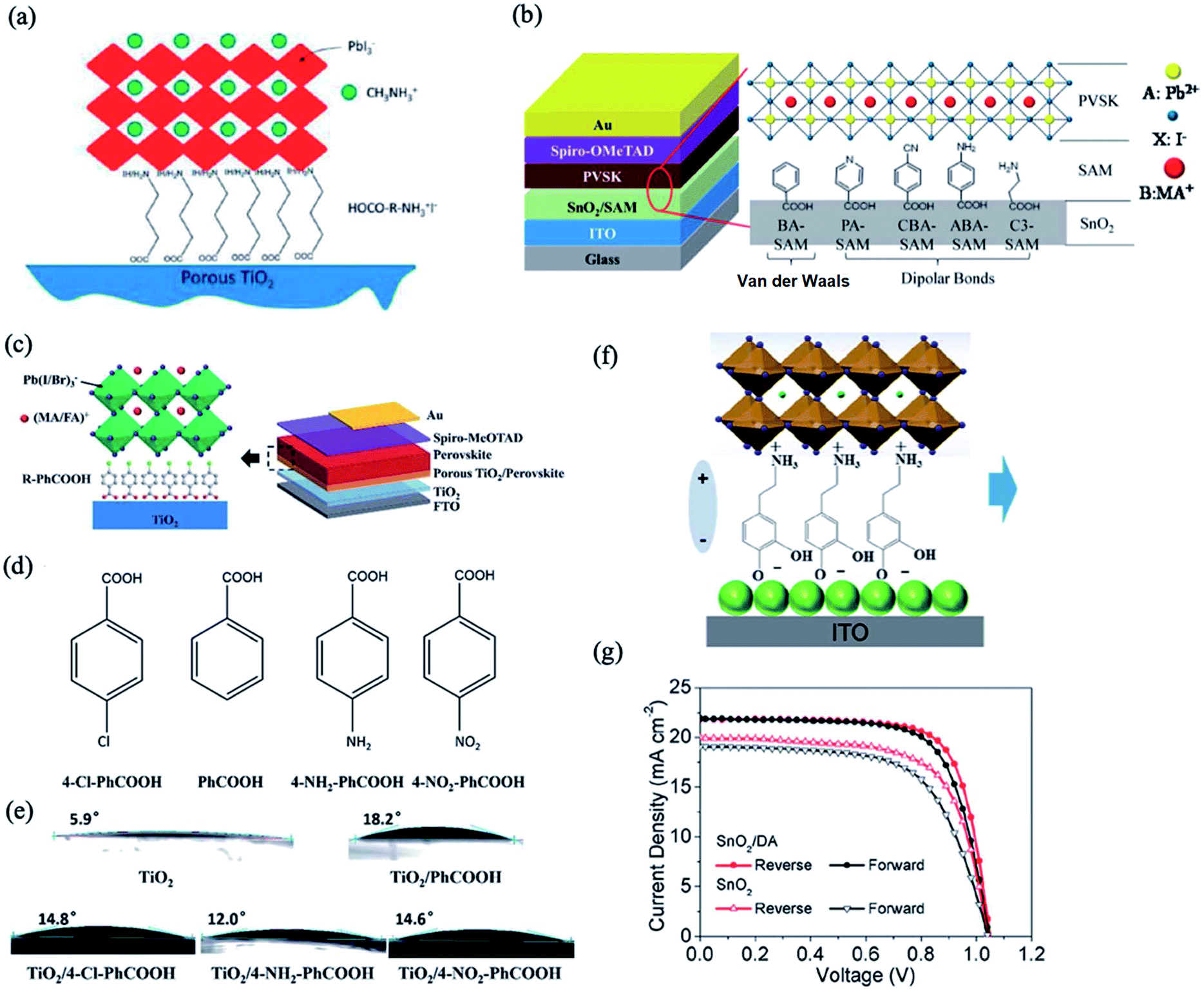 | ||
| Fig. 5 (a) Schematic structure of the TiO2 ETL modified with [HOOC–(CH2)n–NH3]+I−. Reprinted with permission from ref. 72. Copyright 2014 American Chemical Society. (b) Schematics of the device structure (left) and the SAM between the SnO2 and perovskite film (where BA is benzoic acid, PA is 4-pyridine carboxylic acid, CBA is 4-cyanobenzoic acid, ABA is 4-aminobenzoic acid, and C3 is 3-propanoic acid). Reprinted with permission from ref. 73. Copyright 2017 American Chemical Society. (c) Involvement of R–PhCOOH species as modification materials between TiO2 and the perovskite layer and schematic of the device structure. (d) Molecular structures of the R–PhCOOH organic ligands. (e) Contact angles of water on the porous TiO2 layer before and after R–PhCOOH modification. Reprinted with permission from ref. 74. Copyright 2016 Royal Chemical Society. (f) Schematic of the dopamine SAM between the SnO2 ETL and perovskite. (g) J–V curves measured under reverse and forward voltage scanning of the devices deposited on the SnO2 ETL with or without dopamine SAM modification. Reprinted with permission from ref. 75. Copyright 2018 American Chemical Society. | ||
In addition to incorporation of a monolayer of carboxylate-based organic molecules, decorating the ETL surface with organic molecules bearing appended hydroxides as anchoring groups has also emerged as an efficient method to modify the ETL/perovskite interface and improve device performance.75 Dopamine, which contains two functional hydroxyl groups and one amino group, has been introduced as an interfacial modification layer on top of the SnO2 surface (Fig. 5f). It was found that the hydroxyl group anchors to the SnO2 surface, while the terminal amino group regulates the growth of perovskite crystals by hydrogen bonding interactions (N–H⋯I). This modification resulted in better carrier transport and low charge recombination at the SnO2/perovskite interface. Consequently, the device with a dopamine-treated ETL exhibited enhanced stability with a high efficiency of 16.87% compared to the device without ETL modification (Fig. 5g).
Due to the reported instability and degradation of organic molecules under light and heat,76 the modification of the ETL surface with high-temperature stable inorganic compounds was proposed to improve the electron extraction ability to obtain PSCs with high PCE values without J–V hysteresis. Introducing a thin layer of insulator inorganic material at the ETL/perovskite interface suppresses the recombination processes due to inhibition of the back flow of electrons in the presence of the insulator interlayer and the passivation of surface trap states. Importantly, the thickness of the interfacial layer on the ETL must be carefully controlled to ensure minimal loss of charge injection efficiency. Several insulators, such as La2O3,77 Al2O3,78 ZrO2,79 MgO,80 and CsBr,81 have been widely investigated as ultrathin interfacial modifiers for enhancing PSC performance. For example, the modification of the TiO2 ETL with MgO improves the electron lifetime and subsequently retards the electron/hole recombination at the TiO2/CH3NH3PbI3 interface (Fig. 6a).80 The longer recombination time was responsible for enhancing the Voc and FF of MgO-coated TiO2-based PSCs as a result of changes in the band energy diagram (Fig. 6b and c). Li et al. demonstrated that the deposition of CsBr enhances the electron transfer rate from the perovskite to the ETL, leading to significant improvement of the PCE up to 15.3% compared to the control devices with an average efficiency of 11.5%.81 The CsBr modification decreases the work function of TiO2 from 4.07 to 3.90 eV, which is favorable for electron injection (Fig. 6d). The authors also demonstrated that this modification decreased the photocatalytic properties of TiO2 by decreasing the electronic defect density at the ETL/perovskite interface and subsequently improved the UV stability of the perovskite films and devices (Fig. 6e). The PCE of the device subjected to UV irradiation retains more than 70% of its initial value after 20 min; the retention was nearly zero for the control device (Fig. 6f). Interestingly, microscopic analysis revealed that CsBr forms clusters on the c-TiO2 surface rather than a continuous buffer layer film. Thus, it was suggested that the Cs ions inhibit the photocatalytically active sites on the TiO2 and assist in the formation of less defective perovskite at this interface.
 | ||
| Fig. 6 (a) Schematic of the charge transfer mechanism in the MgO-modified TiO2-based PSCs. (b) Band energy diagram of the MgO/TiO2 core–shell NP-based PSC. (c) Voc and FF depending on the MgO layer thickness controlled by the magnesium methoxide concentration. Reprinted with permission from ref. 80. Copyright 2015 The Royal Society of Chemistry. (d) Energy level diagram of the device with the structure of FTO/c-TiO2(CsBr)/perovskite/spiro-OMeTAD/Au. (e) Normalized absorptance at 600 nm wavelength with images of the perovskite film after UV aging with 523 mW cm−2 intensity. (f) The normalized PCE decay of control and CsBr-modified devices upon UV irradiation. Reprinted with permission from ref. 81. Copyright 2016 The Royal Society of Chemistry. | ||
In a similar manner, the TiO2 ETL was partially coated with CuI via a simple one-step spin-coating process and demonstrated highly effective electron extraction ability.82 The p-type character of the deposited islands of CuI on the TiO2 surface changed the energy band diagram. The conduction band of CuI-modified TiO2 increased to −3.93 eV from the value of −4.13 eV for unmodified TiO2, which results in barrier-free contact with perovskite and increased Voc (Fig. 7). It was found that the polarity of the CuI-modified TiO2 surface can pull electrons towards the ETL/perovskite interface with very low recombination. The optimized CuI-modified TiO2-based device shows a high efficiency of 19.0% and negligible hysteresis.
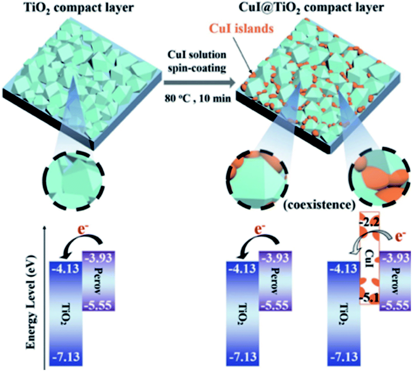 | ||
| Fig. 7 Schematic of the formation of CuI islands on the TiO2 compact layer and subsequent deposition of the perovskite layer. Notably, the electrons from the perovskite move to the exposed TiO2 surface and cannot move to the CuI islands because of their high conduction band energy level. Reprinted with permission from ref. 82. Copyright 2017 Wiley-VCH. | ||
4. Surface engineering of the perovskite/HTL interface
Elegant control of the optoelectronic properties of metal halide perovskites is required to achieve high-efficiency devices.83 The existence of pinholes and incomplete surface coverage on perovskite films can decrease the light absorption and shunt resistance. Moreover, a high density of undesirable defects decreases the charge collection efficiency and increases the charge recombination. The anti-solvent one-step dripping method has been proposed to decrease these effects and prepare highly compact and uniform films.84–86The best performing PSCs still lag behind the theoretical limit of Shockley–Queisser efficiency for a single junction solar cell, possibly due to the electronic defects and high density of grain boundaries (GBs) in the perovskite films.87 Grain boundaries behave as pathways for ion migration and centralized areas of electronic trap states,88–90 which decrease the charge transportation and carrier lifetime.91 Moreover, ion migration at the GBs in perovskite films is supposed to cause current–voltage hysteresis.92 Thus, in order to develop hysteresis-free and high-efficiency PSCs, it is essential to decrease the number of GBs by increasing the grain size of the perovskite crystals.93,94
There are two different methods of thin film perovskite modification, namely physical and chemical. Blowing-gas,95 vacuum-flash,96 hot-casting,97 solvent annealing98 and non-wetting substrates99 are physical modification techniques. In turn, methods such as changing the chemistry of the precursor solutions100–102 and controlling the nucleation and growth by modification of the underlying substrates103 are examples of chemical approaches; these will be exemplified in the following subchapters.
4.1. Thiocyanate additives
The qualities of the perovskite absorber layer, such as surface roughness, grain size, and uniform coverage, play an important role in the PV performance of PSCs.104 Organohalide lead perovskites have high defect tolerance but are not defect impervious.105 It was reported that different thiocyanate ions can control the defect tolerance and charge carrier trapping and decrease the GBs of perovskite thin films.106 Thiocyanate ions (SCN−) were initially used to increase the grain size and enhance the stability of MAPbI3 PSCs against humidity by introducing Pb(SCN)2 in the perovskite precursor solution. The perovskite structure was assumed to be composed of MAPb(SCN)2I or MAPbI3−x(SCN)x.107,108 Further computational and single-crystalline investigations revealed that SCN− ion is not readily incorporated into the 3D MAPbI3 crystal structure but can form 2D layered structures with the formula MA2Pb(SCN)2I2.109–111 In turn, the addition of a small amount of Pb(SCN)2 to the MAPbI3 precursor solution can remarkably improve the crystallinity and grain size of the perovskite thin films.112,113 The SCN− ions were assumed to release gases from the perovskite film in the form of methylamine (CH3NH2) and HSCN during the annealing process. The release of CH3NH2 gas during the perovskite formation improves the crystallinity and increases the grain size of the films (Fig. 8). The accompanying formation of excess PbI2 passivates the defects in the perovskite grain boundaries, leading to a lower recombination rate. Large perovskite crystals enhance the minority carrier lifetime, which subsequently leads to overall improvement of the device performance of PSCs. It was found that a device based on MAPbI3 with a 5% Pb(SCN)2 additive exhibited the best photovoltaic performance, with a PCE up to 18.42% and negligible hysteresis.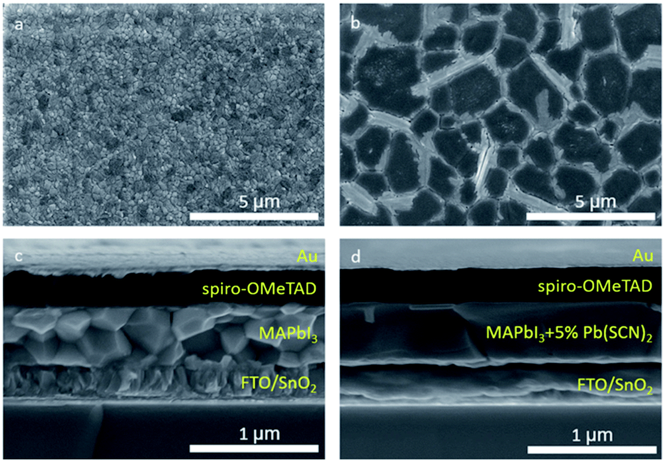 | ||
| Fig. 8 Top-view SEM images of MAPbI3 films (a) without and (b) with 5% Pb(SCN)2 additive deposited on SnO2 ETL. Cross sectional SEM images of the completed devices using MAPbI3 (c) without and (d) with 5% Pb(SCN)2 additive. Reprinted with permission from ref. 112. Copyright 2016 Wiley-VCH. | ||
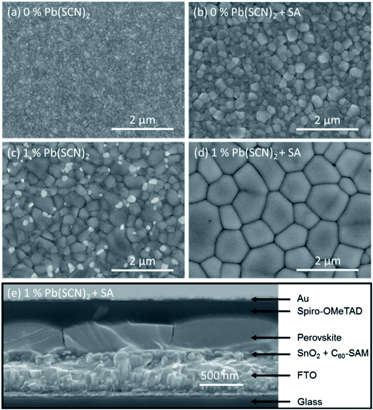
In a similar manner, Chiang et al. investigated the influence of the SCN− ion on the morphological and optoelectronic properties of FA0.9Cs0.1PbI3 perovskite thin films.114 It was demonstrated that the addition of 5 and 10 mol% Pb(SCN)2 additive significantly enlarges the grain size of perovskite films and increases the carrier lifetime. In turn, Yu et al. studied the effects of Pb(SCN)2 additive on the performance of wide bandgap mixed-cation and mixed-halide FA0.8Cs0.2Pb(I0.7Br0.3)3 perovskite solar cells.115 Although the grain size increases as the concentration of Pb(SCN)2 additive increases, the concomitant formation of excess residual PbI2 nanorods on the perovskite films deteriorates the device performance. Surprisingly, there was no notable change in the bandgap of the FA0.8Cs0.2Pb(I0.7Br0.3)3 thin film. It was found that the combination of 1.0 mol% Pb(SCN)2 additive and the solvent annealing procedure during thin film formation led to significantly increased grain sizes (from 66 ± 24 to 1036 ± 317 nm) without formation of excessive PbI2 (Fig. 9), and the mean carrier lifetime showed a 3-fold growth from 330 ns to over 1000 ns. The average PCE of the FA0.8Cs0.2Pb(I0.7Br0.3)3-based PSCs increased from 13.44 ± 0.48 to 16.46 ± 0.37 using 1.0 mol% Pb(SCN)2 additive and a solvent annealing procedure. In other work, the addition of Pb(SCN)2 to a triple-cation mixed-halide perovskite, FA0.7MA0.2Cs0.1Pb(I5/6Br1/6)3, not only improved the crystallinity and optical absorption of the perovskite but also hindered the formation of morphological defects and non-radiative recombination.116 Moreover, the Pb(SCN)2-treated perovskite film exhibited remarkably high moisture and thermal stabilities, leading to a high PCE of 14.09% for planar-solar cells with alleviated hysteresis.
 | ||
| Fig. 9 Top-view SEM images of FA0.8Cs0.2Pb(I0.7Br0.3)3 perovskite thin films: (a) reference; (b) no Pb(SCN)2 additive with solvent annealing; (c) with 1.0 mol% Pb(SCN)2 additive but no solvent annealing; and (d) with combined 1.0 mol% Pb(SCN)2 additive and solvent annealing. (e) Cross-sectional SEM image of the device with the perovskite layer synthesized by the combined 1.0 mol% Pb(SCN)2 additive and solvent annealing process. The white grains in (c) are PbI2 precipitates. Reprinted with permission from ref. 115. Copyright 2017 American Chemical Society. | ||
In addition to SCN− ions, the cations used in the fabrication process play an important role in the quality of perovskite films.117–119 The introduction of alkali metal ions (Na+ or K+) was stated to effectively improve the growth of perovskite films with fewer GBs and trap states.120–122 Zhang et al. introduced potassium thiocyanate (KSCN) into the perovskite precursor solution and fabricated hysteresis-free PSCs with high photovoltaic performance.123 The grain size of the MAPbI3 perovskite film increases with increasing KSCN content due to the positive synergistic effect of SCN− and K+ ions. In this process, CH3NH2 and HSCN gases escaped and small amounts of potassium iodide (KI) and PbI2 passivated the perovskite layer. As a result, the PCE of MAPbI3 PSCs increased from 14.72% to 19.12% using 1.0 mol% additive KSCN under forward bias with negligible hysteresis (Fig. 10).
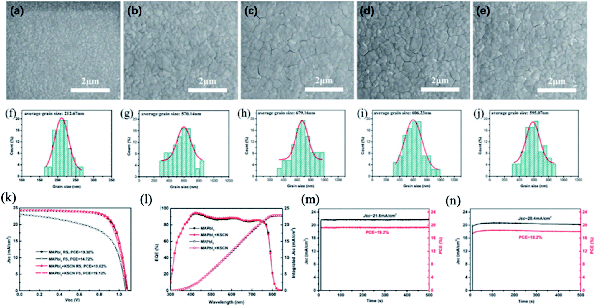 | ||
| Fig. 10 Top-view SEM images of MAPbI3 films with different concentrations of KSCN: (a) 0 mol%, (b) 0.5 mol%, (c) 1 mol%, (d) 2 mol%, and (e) 3 mol%; (f)–(j) are the corresponding statistical distributions of the MAPbI3 grain size. J–V curves of the PSCs with and without 1 mol% KSCN tested at a scan rate of 50 mV s−1 under 1 sun AM 1.5 G. (k) EQE and integrated Jsc spectra of the PSCs with and without 1 mol% KSCN (l). The steady-state output of the PSCs with (m) and without (n) 1 mol% KSCN measured at the maximum power point under 1 sun AM 1.5 G, respectively. Reprinted with permission from ref. 123. Copyright 2019 The Royal Society of Chemistry. | ||
Other relevant work demonstrated that treatment of the MAPbI3 surface with guanidinium thiocyanate (GUTS) converts its nanometer-scale grains into a micron-sized grain film.93 The grain size of the MAPbI3 films increases proportionally with the concentration of GUTS, decreasing the number of barriers (GBs) for charge transport between the anode and cathode in PSCs (Fig. 11a–f). The remarkable change in morphology is due to the initial stages of the Ostwald-type ripening mechanism.124 During this process, when GUTS/IPA solution is added to the surface of the MAPbI3 film, less stable small crystals of MAPbI3 with high surface energies dissolve partially into the IPA and transfer their mass for growth of large, stable crystals. When comparing I− and SCN− anions, the SCN− ion has stronger interaction with Pb2+; thus, the Ostwald ripening process is very effective for GUTS/IPA treatment.125 The concentration of the GUTS precursor plays a key role in the optical properties, surface potential, crystal structure and morphology of the perovskite film. The PCE of MAPbI3 PSCs was increased from 12.7% to 15.2% using a 4 mg ml−1 concentration of GUTS/IPA. Moreover, devices with optimized GUTS additive showed better moisture stability and less-pronounced hysteresis in the J–V curve than untreated PSCs (Fig. 11g and h).
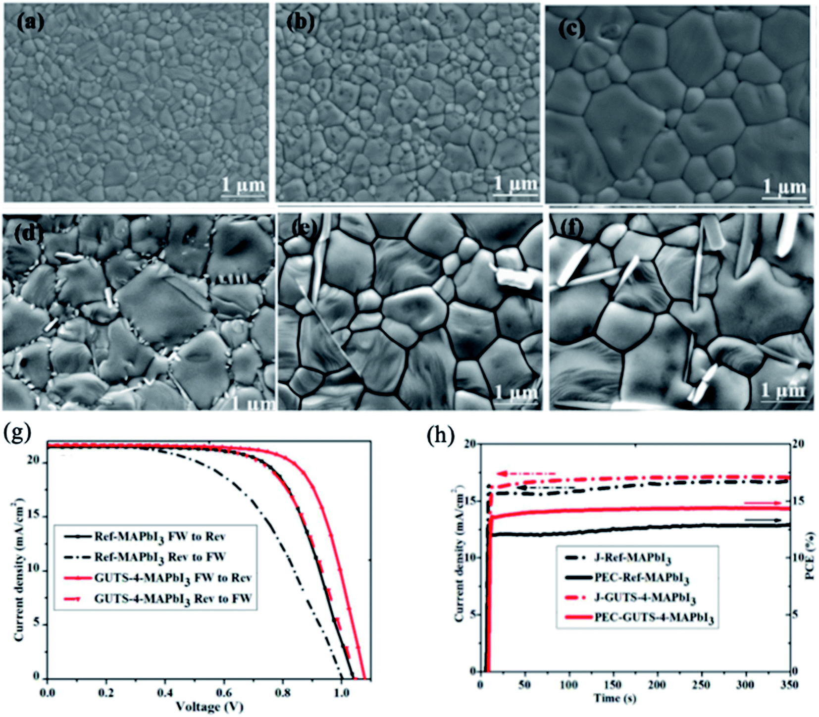 | ||
| Fig. 11 (a) Control MAPbI3 film and films treated with different concentrations of GUTS/IPA solution: (b) 2 mg mL−1, (c) 4 mg mL−1, (d) 6 mg mL−1, (e) 8 mg mL−1, (f) 10 mg mL−1. (g) J–V curves of MAPbI3 PSCs with and without GUTS-4 post-treatment under reverse and forward bias. (h) Moisture stability of the MAPbI3 cell (black curve) and the GUTS-4-treated MAPbI3 cell (red curve). The solar cells were stored in a desiccator with a relative humidity of ∼33% in the dark. Reprinted with permission from ref. 93. Copyright 2017 Elsevier. | ||
4.2. Using excess amounts of PbI2 or MAI additives
Differences in the stoichiometry of the perovskite precursors in solution were found to play a positive role in decreasing the recombination at the GBs and improving the charge carrier transfer. It was observed that a small excess of PbI2 can decrease defect recombination in MAPbI3 (ref. 101, 126 and 127) or mixed-cation and mixed-halide perovskite layers.128,129 There are three techniques to passivate perovskite GBs using PbI2 layers. They are based on self-induced formation of PbI2 by water vapor130–132 or thermal treatment,133–135 a nonstoichiometric perovskite precursor solution containing excess PbI2 (ref. 127, 129, 136–138) and incomplete reaction of PbI2 through a vapor reaction method.139–141 The advantageous effect of PbI2 is realized by balancing the passivation of the perovskite film with the decrease of the electron transfer. It was reported that upon passivation by PbI2, the carrier lifetime increased and the charge carrier trap density of TiO2 decreased from 1019 cm−3 to 1016 cm−3.142–144Various possible passivation mechanisms of PbI2 were proposed based on the interface between the perovskite film and PbI2 phase.129 One hypothesis suggests that the band edge matching between TiO2, PbI2, and the perovskite or surface passivation are responsible for the decreased hole recombination (Fig. 12a). Another hypothesis is that PbI2 at the perovskite/HTL interface facilitates hole injection and decreases the recombination rate (Fig. 11b). If the energy band alignment is mismatched or the PbI2 layer is too thick, it may block the carriers and thus insulate individual grains (Fig. 12c and d). PbI2 phase may also control the stoichiometry of the perovskite composition at the GBs. The inner composition of perovskite grains may be insensitive to small changes in the overall stoichiometry. Consequently, the GBs must be highly sensitive to the overall composition. This can affect the dangling bonds, doping, ion migration and defect states. Yang's group reported that PbI2 minimizes the number of trapping states by filling the perovskite GBs and changing the grain-to-grain boundary-bending from downward to upward, thus decreasing the recombination between holes and electrons from the HTL and the perovskite, respectively (Fig. 12e).133 If too much PbI2 is present in the GBs, it can act as an insulating layer rather than a passivation layer. Moreover, it was demonstrated that the presence of excess PbI2 results in faster degradation of the perovskite layer upon exposure to illumination and humidity compared to perovskite films without excess PbI2.137 Thus, optimization of the deposition process for perovskite films with excess PbI2 should be carefully undertaken, and the effects of the decomposition of the perovskite layer should be considered.
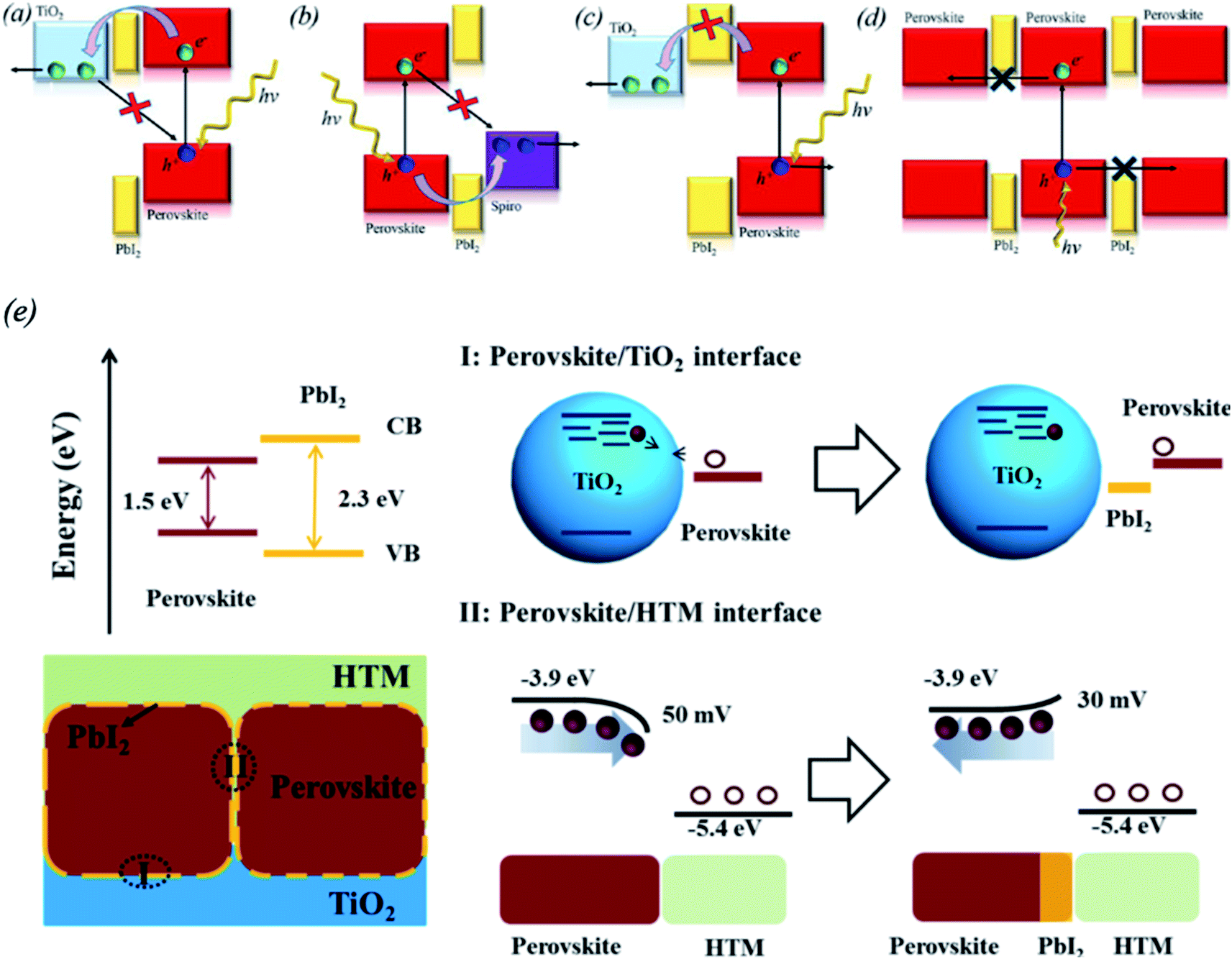 | ||
| Fig. 12 Consequences of excess PbI2 in perovskite films related to possible energy alignments suggested in the literature and an artistic illustration of different grain boundary characters as a function of the overall stoichiometry. (a) PbI2 as a passivation layer at the back contact. (b) PbI2 as a passivation layer next to the hole-selective layer. (c) PbI2 as an electron blocking layer next to the back contact. (d) PbI2 as a charge carrier barrier between perovskite grains. Reprinted with permission from ref. 129. Copyright 2016 American Chemical Society. (e) Proposed mechanism for PbI2 passivation in CH3NH3PbI3 films. The perovskite/HTL interface is described on the bottom right; the presence of PbI2 changes the grain-to-grain boundary bending from downward to upward, which helps decrease recombination between the electrons from perovskite and the holes from HTL. Reprinted with permission from ref. 133. Copyright 2014 American Chemical Society. | ||
Similar to the effect of excess PbI2, the GBs can be passivated by excess methylammonium iodide (MAI).145,146 The excess MAI can modify the grain surface of the perovskite films by forming self-assembled GBs on the MAPbI3 film, leading to improved PV performance and decreased hysteresis of MAPbI3 PSCs. The c-AFM images of pure MAPbI3 and modified perovskite with 0.06% excess MAI showed increased conductivity due to MAI passivation. The MAPbI3 PSCs with a 0.6% excess of MAI showed the best efficiency, up to 20.4%, measured under reverse scan.145 The analysis of MAI-rich perovskite films with confocal PL microscopy revealed that excess MAI enhances the PL intensities and carrier recombination lifetimes in both the grain interiors and GBs.146
4.3. Using chloride and bromide additives
The PCE and stability of MAPbI3 PSCs can be enhanced by substitution of various amounts of iodine with chloride or bromide ions.147–151 Chen et al. reported that the introduction of MACl into the perovskite films can improve the grain size up to 1 μm.151 The Cl− incorporation does not affect the carrier transportation in the perovskite film and improves the PV performance of the device. Using a 1![[thin space (1/6-em)]](https://www.rsc.org/images/entities/char_2009.gif) :10 weight ratio of MACl/MAI, the PCE of the resulting MAPbI3−xClx PSC increased from 14.12% to 17.91%. A series of MAPbI3−xClx perovskites with various Cl contents was also prepared through gas/solid reactions between MA gas and HPbI3−xClx (x = 0–1).152 Low Cl doping was found to significantly enhance the grain-size growth of MAPbI3−xClx crystals and improve the PV performance. In turn, for Cl contents higher than 0.1 (x > 0.1), a separate perovskite phase of MAPbCl3 formed, which inhibits the electron transfer and deteriorates the photovoltaic performance (Fig. 13a–d). Recently, Li et al. investigated the effects of the MACl/MAI ratio (0:1, 0.5:1, 1:1 and 2:1) on the morphology of perovskite films and the interfacial charge transfer dynamics of devices with both planar and mesoporous architectures.153 It was found that chloride doping with a 2:1 ratio leads to larger grain size and faster interfacial charge injection rates in the planar architecture compared to the mesoporous architecture, leading to significant improvement of the PV performance. The introduction of MACl into the perovskite precursor solution also appears to be a convenient method to enlarge the grain size of the triple A-cation (MA/FA/Cs) perovskite composition.154 In general, the triple A-cation perovskite films are composed of small grains (∼200 nm) because the presence of Cs ions leads to fast nucleation of perovskite crystals. The modification of triple A-cation perovskite with MACl improved the crystallinity as well as the grain size of the film up to 1 μm. It was found that MACl does not affect the absorption or photoluminescence properties of perovskite films; its role is to aid the formation and growth of crystals rather than their incorporation in the perovskite lattice.
:10 weight ratio of MACl/MAI, the PCE of the resulting MAPbI3−xClx PSC increased from 14.12% to 17.91%. A series of MAPbI3−xClx perovskites with various Cl contents was also prepared through gas/solid reactions between MA gas and HPbI3−xClx (x = 0–1).152 Low Cl doping was found to significantly enhance the grain-size growth of MAPbI3−xClx crystals and improve the PV performance. In turn, for Cl contents higher than 0.1 (x > 0.1), a separate perovskite phase of MAPbCl3 formed, which inhibits the electron transfer and deteriorates the photovoltaic performance (Fig. 13a–d). Recently, Li et al. investigated the effects of the MACl/MAI ratio (0:1, 0.5:1, 1:1 and 2:1) on the morphology of perovskite films and the interfacial charge transfer dynamics of devices with both planar and mesoporous architectures.153 It was found that chloride doping with a 2:1 ratio leads to larger grain size and faster interfacial charge injection rates in the planar architecture compared to the mesoporous architecture, leading to significant improvement of the PV performance. The introduction of MACl into the perovskite precursor solution also appears to be a convenient method to enlarge the grain size of the triple A-cation (MA/FA/Cs) perovskite composition.154 In general, the triple A-cation perovskite films are composed of small grains (∼200 nm) because the presence of Cs ions leads to fast nucleation of perovskite crystals. The modification of triple A-cation perovskite with MACl improved the crystallinity as well as the grain size of the film up to 1 μm. It was found that MACl does not affect the absorption or photoluminescence properties of perovskite films; its role is to aid the formation and growth of crystals rather than their incorporation in the perovskite lattice.
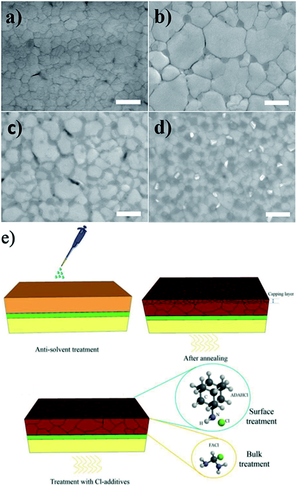 | ||
| Fig. 13 SEM images of (a) MAPbI3, (b) MAPbI2.95Cl0.05, (c) MAPbI2.67Cl0.33 and (d) MAPbI2Cl1 perovskite films annealed for 5 min at 100 °C. The scale bar is 500 nm. Reprinted with permission from ref. 152. Copyright 2017 Wiley-VCH. (e) Schematic of perovskite films fabricated by the antisolvent method on SnO2-coated FTO glass before and after treatment with FACl and Cl-based adamantane additives. Reprinted with permission from ref. 155. Copyright 2019 Wiley-VCH. | ||
Formamidinium chloride (FACl) has also been used as an alternative chlorine source to improve the crystallinity and grain size of perovskite.155 The addition of FACl to the precursor solution removes the small-grained perovskite capping layer and suppresses the formation of bulk and surface defects, providing a perovskite film with enhanced crystallinity and large grain sizes of over 1 μm (Fig. 13e). Moreover, FACl helps replace the MA cations with FA cations in the perovskite composition because the Cl ions leave the perovskite film during the annealing process in the form of MACl, which improves the stability of PSC devices as well. The combined effects of bulk modification and surface passivation of the perovskite film with Cl-based adamantane resulted in a high PCE of 21.2% with improved stability.
The addition of a small amount of guanidinium chloride (GACl) to a MAPbI3 precursor solution was also found to play a positive role in the optoelectronic properties of perovskite films and the enhancement of the PCE.156 In particular, the GACl-based perovskite film exhibited enhanced PL intensity and charge carrier lifetime compared to the pristine MAPbI3 film, indicating decreased trap density in the film. The authors reported that GA cation is not incorporated into the perovskite crystal lattice due to the larger ion radius but rather resides at the grain boundaries and passivates the under-coordinated iodine species. Notably, further solid-state NMR studies provided atomic-level evidence that GA cation can be directly incorporated into the MAPbI3 crystal lattice.157 Wang et al. systematically studied the effects of the various amine hydrochloride additives with different sizes and space structures, i.e. 2,2,2-trifluoroethylamine hydrochloride, benzenamine hydrochloride, 3-chloropropylamine hydrochloride, and diethylamine hydrochloride, on the MAPbI3 perovskite film-forming process.158 These organic cations enhanced the crystallinity and grain size of the perovskite films and, consequently, the performance of the solar cells.
To optimize the PV performance of PSCs, the electron injection and carrier recombination must be optimized. It was found that the partial substitution of iodide with bromide ions in the perovskite composition may also increase the grain size,159–161 optimize the crystallization rate162 and tune the band gap from 1.5 to 2.2 eV.147,163,164 Kim et al. studied the effects of the Br content on the local electrical properties of the MAPb(I1−xBrx)3 perovskite thin films using Kelvin probe force microscopy (KPFM) and conductive atomic force microscopy (c-AFM).165 It was observed that a region with highly positive charge appeared in the GBs, and the local current (<50 pA) flows through most of the grains for the MAPb(I1−xBrx)3 (x = 0.12) perovskite films. Remarkable potential barrier bending occurs at the GBs, and the positively charged GBs in the Br-passivated perovskite thin films can produce downward energy band bending. Due to the charged GBs, the electrons move towards the TiO2 side and holes are attracted to the HTL side (Fig. 14). Thus, recombination of charges between the ETL and HTL is suppressed, and the charge carriers are separated.166
 | ||
| Fig. 14 (a) Structure of mesoporous TiO2 with a mixed halide perovskite absorber. (b) Schematic band diagram near the GBs in Br-containing MAPb(I0.88Br0.12)3 thin films. Reprinted with permission from ref. 165. Copyright 2015 American Chemical Society. | ||
This work demonstrates that the approach of using organic amine hydrochloride/hydrobromide additives has great potential in the production of high-quality perovskite films for low-cost and high-performance devices.
4.4. Using solvent additives
To decrease the intrinsic defect density in perovskite films, various solvent additives are often added to the precursor solution.167,168 The crystallization rate and growth of perovskite crystals was found to be controlled by incorporating bidentate halogenated additives into the precursor solution. For example, 1,8-diiodooctane (DIO) encourages homogenous nucleation and crystallization of MAPbI3−xClx perovskite films, which facilitates the charge transfer between the charge transporting interlayers and the perovskite absorber.169 This additive was stated to temporarily chelate with Pb2+ during the crystal growth and modulate the crystallization kinetics. In a similar manner, bidentate halogenated additives with different alkyl chain lengths and end-groups, i.e. 1,4-diiodobutane (1,4-DIB), 1,10-diiodinedecane (1,10-DID), 1,4-dibromobutane (1,4-DBrB), and 1,4-dichlorobutane (1,4-DClB), enhanced the crystallization and substrate coverage of perovskite thin films on PEDOT:PSS substrates.170 The changes in crystallization dynamics induced by alkyl halides were attributed to the cooperative effects of modulated solvent–solute interactions between the alkyl halides and Pb2+ and the cleaved C–X (X = Cl, Br, I) bonds during thermal annealing (Fig. 15a). The grain sizes of the perovskite thin films and overall device performance were found to be significantly dependent on how readily the C–X bond is cleaved, and the device made from the solution containing 1% 1,4-DIB showed the best photovoltaic performance.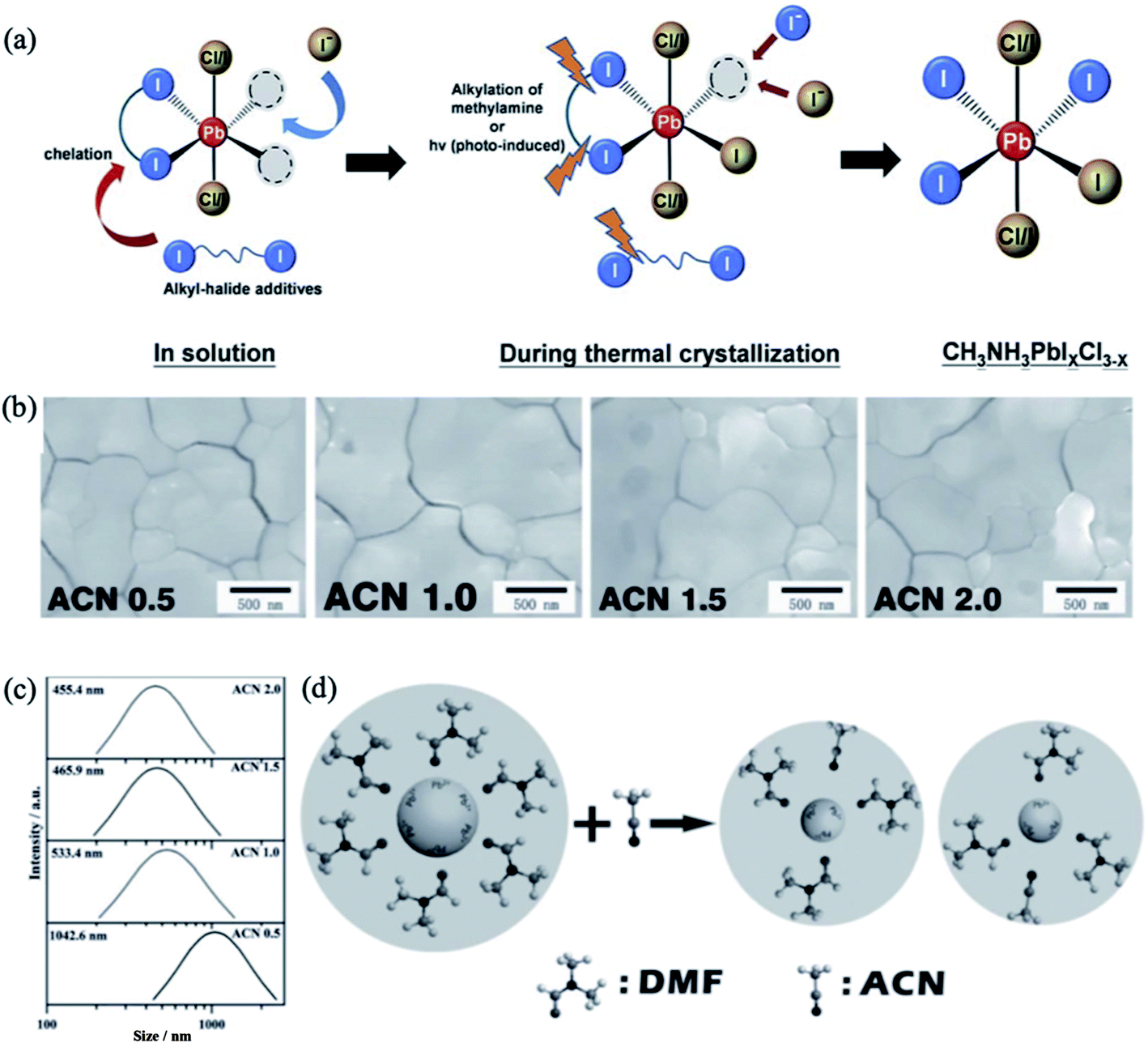 | ||
| Fig. 15 (a) Illustration of the roles of alkyl-halide additives during perovskite crystallization. Reprinted with permission from ref. 170. Copyright 2015 The Royal Society of Chemistry. (b) SEM images of the perovskite thin films fabricated with different concentrations of the ACN additive. (c) Size distribution of the PbI2–DMF particles. (d) Mechanism for the formation of the PbI2–DMF cluster manipulated by the ACN additive. Reproduced with permission from ref. 171. Copyright 2016 Wiley-VCH. | ||
Li et al. demonstrated that the introduction of weakly coordinating solvent molecules, e.g. acetonitrile (ACN), into the PbI2/DMF solution effectively enhances the grain morphology and roughness of MAPbI3 perovskite thin films.171 An optimized ratio of ACN/PbI2 successfully affects the interaction between PbI2 and DMF and modifies the nucleation dynamics, leading to the formation of large grains. The grain size of the perovskite films was found to increase with increasing ACN concentration (Fig. 15b). As revealed by dynamic light scattering (DLS) analysis, the radius of the PbI2–DMF particles decreases with increasing ACN concentration due to partial replacement of DMF molecules by ACN and concomitant formation of ACN–PbI2–DMF adducts, which are much smaller then PbI2–DMF particles (Fig. 15c). The low boiling point of ACN generates pores in the PbI2 film during the annealing process; these pores can act as nucleation centers for the newly formed perovskite. Subsequent deposition of MAI on these nucleation centers favors the formation of a smooth perovskite film with a large grain size (Fig. 15d). Similarly, the proper addition of weakly coordinating isopropanol (IPA) to a precursor solution containing MAI/PbI2 resulted in the formation of uniform perovskite films with low defect densities.172 In addition, the device with IPA additive exhibited better photovoltaic performance and higher stability against moisture compared with the reference material.
Moisture is known to be a critical factor for perovskite stability because water can decompose the structure of perovskite into its starting precursors.173 However, the controlled addition of water to the precursor solution can assist the nucleation and grain growth of perovskite films. The use of H2O as a solvent additive in PbI2/DMF precursor solution resulted in the formation of good quality PbI2 films on PEDOT:PSS-coated ITO.174 As shown in Fig. 16a, full-coverage PbI2 films were obtained only when the PbI2/DMF solution contained 2 to 3 wt% H2O. Further deposition of MAI on the water-modified PbI2 layer led to the crystallization of a smooth, highly crystalline and compact perovskite MAPbI3 film with improved light absorption and charge carrier transportation. As a result, impressive PCEs of 18% were observed for the inverted devices fabricated using 2% H2O additive. Further improvement in performance was achieved by adding controlled amounts of H2O to both the PbI2/DMF and MAI/IPA precursor solutions and DMF vapour post-treatment.175 This synergistic strategy resulted in crystallization of a high-quality 500 nm thick MAPbI3 layer with horizontal grain sizes up to 3 μm. The optimized inverted device yielded a very high PCE of 20.1% and an FF of 0.83. Incorporating a proper amount of water into a DMF-based perovskite precursor solution containing MAI and PbCl2 also improved the crystallization of perovskite thin films with good coverage and smooth morphologies (Fig. 16b).176 Systematic analysis of the modified perovskite films indicated that the 2% H2O additive-based perovskite sample afforded a more continuous and large-grained perovskite film. The higher vapor pressure and lower boiling point of H2O aided the formation of large crystals. Consequently, the optimized water additive-based device showed a high PCE of 16.06% and improved cell stability under ambient conditions compared with the reference cell (Fig. 16c).
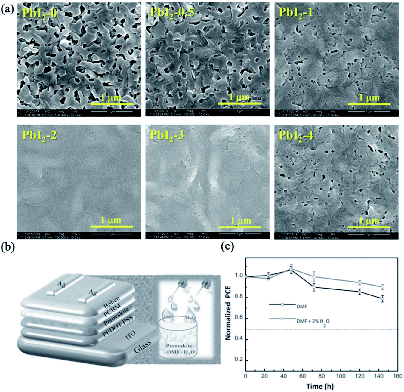 | ||
| Fig. 16 (a) SEM images of PbI2 films prepared from PbI2/DMF solutions containing various amounts of H2O additive. Reprinted with permission from ref. 174. Copyright 2015 Royal Society of Chemistry. (b) Device structure and schematic of the incorporation of water additive into DMF-based perovskite precursor solutions. (c) Device stabilities of DMF and DMF + 2% H2O-based PSCs under ambient conditions. Reprinted with permission from ref. 176. Copyright 2015 Wiley-VCH. | ||
4.5. Lewis acid/base additives
An efficient strategy to passivate surface defect states on perovskite films is the use of Lewis acids or Lewis bases to passivate surface traps. For example, iodopentafluorobenzene (IPFB) was tested as a Lewis acid to passivate excess iodine ions on the surface of MAPbI3−xClx films (Fig. 17a).177 Under-coordinated iodide anions may serve as hole-traps at the perovskite/HTL interface in PSCs (Fig. 17b). These hole-traps lead to faster recombination of charge carriers and decreased charge density within the perovskite/HTL interface. The use of IPFB resolved this issue by screening the electrostatic charge from the under-coordinated halide ions, resulting in decreased non-radiative recombination and enhanced photovoltaic performance. Other work demonstrated that treatment of MAPbI3−xClx films with Lewis bases such as thiophene or pyridine can also significantly decrease the rate of nonradiative recombination in perovskite films (Fig. 17c).178 During the annealing process, the halide and methylammonium ions can leave the perovskite film, forming under-coordinated Pb atoms that act as electronic trap states both on the crystal surface and at the grain boundaries. To neutralize the excess positive charges in the perovskite crystal, the selected thiophene or pyridine molecules donate electron density to the undercoordinated Pb ions, forming coordination bonds (Fig. 17d). As a result, the efficiencies of MAPbI3−xClx PSCs were enhanced from 13% to 15.3% and 16.5% after thiophene and pyridine treatments, respectively.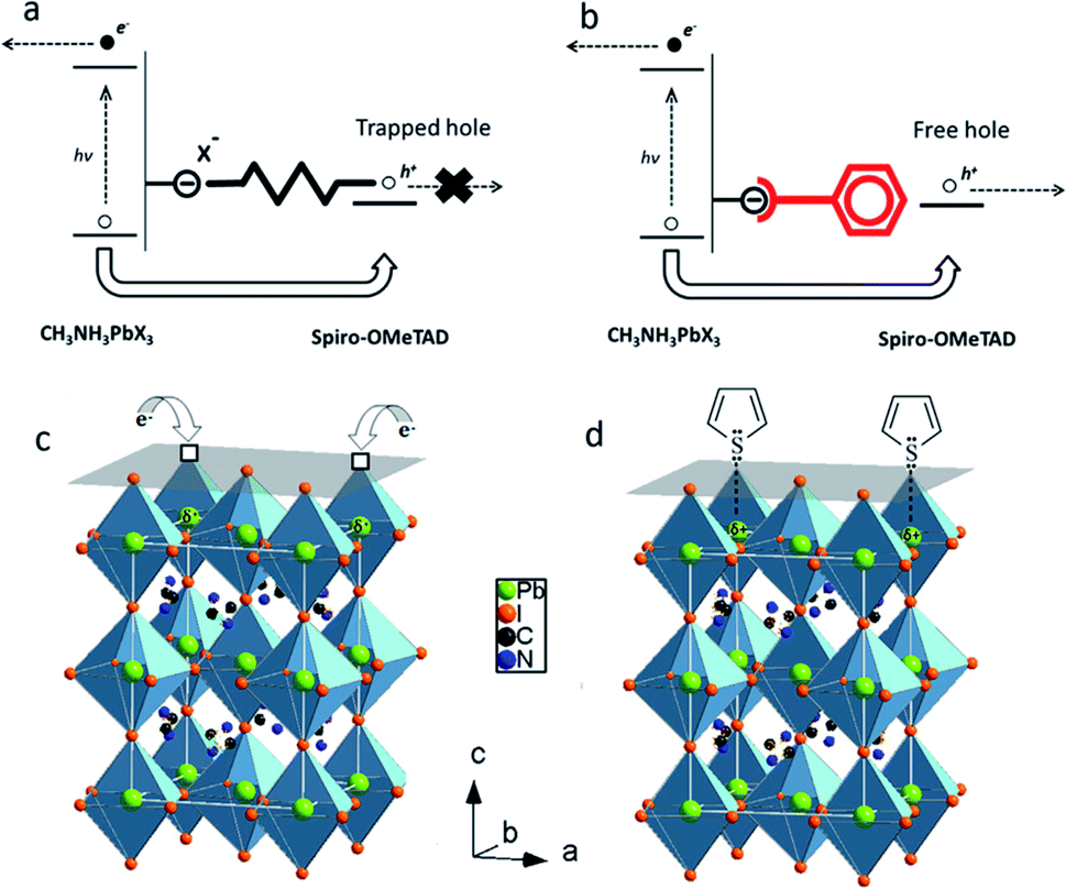 | ||
| Fig. 17 (a) Schematic of the electrostatic interaction between an under-coordinated halide ion on the perovskite surface and a hole injected in spiro-OMeTAD. (b) Schematic of the electrostatic screening of the halide ion via halogen bond complexation of iodopentafluorobenzene (IPFB) on the perovskite surface, which can stop trapping of the holes. Reproduced with permission from ref. 177. Copyright 2014, American Chemical Society. (c) Loss of iodine at the surface of the perovskite leads to vacancy sites (hollow boxes) and a resulting net positive charge residing on the Pb atom (shown in green). Photogenerated electrons can then fall into this Coulomb trap site, thus neutralizing the charge and stabilizing the crystal. (d) Schematic of the donation of thiophene electron density to Pb ions to form coordinate or dative covalent bonds, effectively neutralizing the excess positive charge in the crystal. Reproduced with permission from ref. 178. Copyright 2014, American Chemical Society. | ||
Wen et al. systemically investigated the relationship between the device efficiency and stability and the type of employed 3-alkylthiophene derivative (thiophene, 3-methylthiophene, 3-ethylthiophene, 3-butylthiophene, 3-hexylthiphene and 3-dodecylthiophene).179 These molecules contain delocalized conjugated π systems and hydrophobic alkyl groups that can enhance the charge transfer and collection at the perovskite/HTL interface and protect the bulk perovskite from humidity. It was found that the 3-hexylthiphene post-treatment significantly enhanced both the stability and performance of Cs0.05FA0.81MA0.14PbBr0.45I2.55-based PSCs. Another example of a π-conjugated Lewis base, indacenodithiophene end-capped with 1.1-dicyanomethylene-3-indanone (IDIC), has also been shown to be effective in passivating undercoordinated Pb ions on the MAPbI3 surface (Fig. 18a).180 Due to its n-type semiconducting properties, IDIC simultaneously enhances the charge transfer in perovskite films, while the Lewis base end groups (carbonyl and cyano groups) of IDIC passivate the traps (Fig. 18b and c). Hence, MAPbI3/IDIC-based solar cells yielded stabilized PCEs of up to 19.5% with hysteresis-free and stable outputs compared with reference devices without IDIC-based passivation. This study opens up a route to design new π-conjugated Lewis bases by combining various organic π-conjugated structures (e.g., aromatic fused rings, oligothiophenes) and Lewis base substituent groups (e.g., thiocyanato, sulfhydryl, carbonyl) to achieve defect passivation and further improve both the efficiency and stability of PSCs.181,182
 | ||
| Fig. 18 (a) Molecular structure of IDIC. (b) Schematic of the interaction of the π-conjugated Lewis base and Pb ions. (c) Diagram depicting the formation of a dative covalent bond between two atoms and passivation of trap states. Reprinted with permission from ref. 180. Copyright 2017 Wiley-VCH. | ||
4.6. Hydrophobic additives
Some organic insulating polymers consisting of hydrophobic groups such as poly(ethylene terephthalate) (PET), Teflon,183,184 polystyrene (PS),183 polyvinylidene-trifluoroethylene copolymer (PVDF-TrFE), poly(4-vinylpyridine) (PVP)183,185 and even ionic liquids186 can diffuse into the GBs and cover the surface of the perovskite thin films. These polymers deposited on the perovskite films form a ultrathin tunneling layer that suppresses charge recombination by separating the excess electrons and holes in the electron transport layer and perovskite layer.183 Moreover, these tunneling layers may act as encapsulation layers to protect perovskite films from decomposition caused by moisture. For example, trichloro(3,3,3-trifluoropropyl)silane appears to be an efficient agent to act as a tunneling layer to fabricate water-resistant devices. A very small amount of H2O can trigger the hydroxylation of silanes to form silanols; these subsequently undergo cross-linking reactions, forming Si–O–Si (siloxane) bonds (Fig. 19a). This layer protects the perovskite film underneath it, and the resulting devices show much better resistance to water damage. In other work, Zuo et al. used polymer functionalized with a Lewis base pyridine group, poly(4-vinylpyridine) (PVP), as an agent to passivate the undercoordinated Pb2+ ions and improve both the device efficiency and the stability of PSC cells.187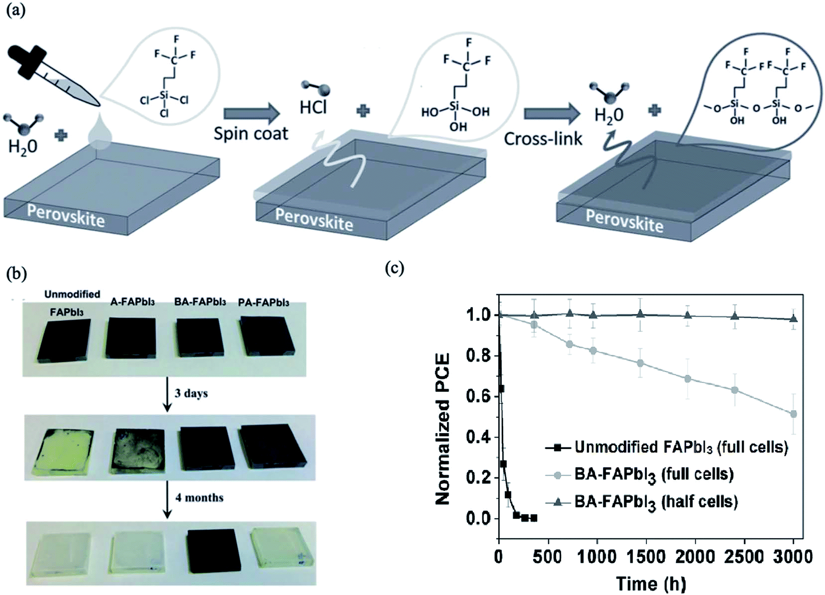 | ||
| Fig. 19 (a) Schematic showing the cross-linking process of the fluoro-silane layer on perovskite films. Reprinted with permission from ref. 183. Copyright 2016 Wiley-VCH. (b) Images of unmodified FAPbI3, A-FAPbI3, BA-FAPbI3 and PA-FAPbI3 films under different durations (fresh, 3 d, 4 months) of exposure under 50 ± 5 RH% air. (c) Moisture stability of unmodified FAPbI3 and BA-FAPbI3 devices under air exposure (50 ± 5 RH%). “Half cells” means that only the BA-FAPbI3 films on the TiO2/FTO substrates were exposed to air and that the spiro-MeOTAD and Au layers were deposited onto the films before the J–V measurements. Reprinted with permission from ref. 188. Copyright 2016 Wiley-VCH. | ||
In addition to organic polymers, the use of hydrophobic amine functional molecules to passivate perovskite films can be regarded as efficient method for enhancing the stability against moisture and improving the electronic properties of PSCs.188 Wang et al. tested aniline (A), phenethylamine (PA) and benzylamine (BA) for passivation of FAPbI3 perovskite films. The selected molecules contain benzene rings, whose π-conjugation structures favor charge transport, while amino groups may be anchored to the Pb–I framework through coordination with the Pb ions or hydrogen bonding with the iodide ions. The authors observed that only benzylamine can stabilize the perovskite films for more than four months in moist air (Fig. 19b). The benzylamine-modified device showed a longer carrier lifetime and improved performance and stability under air exposure (Fig. 19c).
4.7. Surface passivation by oxygen and silica
Tian et al. observed a synergistic passivation effect of a perovskite crystal surface by oxygen using super-resolution optical imaging and PL microscopy.189 The PL intensities of both the small (<100 nm) and large crystals (several micrometers) increase with increasing irradiation time in air, while the PL intensities of the samples in an argon environment are almost constant (Fig. 20a and b). In argon atmosphere, the PL lifetime of the small crystals is much longer than that of the large crystals (Fig. 20c). This evidence reveals that in air, oxygen acts as a reactant to passivate the traps of small crystals rapidly and efficiently. The enhancement of the PL intensity over time was found to vary greatly depending on the measurement position within one crystal when the PL signals of isolated micrometer-sized crystals were investigated at high spatial resolution. Light-induced curing in the presence of oxygen causes enhancement of the perovskite photoluminescence. In other work, the same authors hypothetically proposed that the trap sites are responsible for non-radiative charge recombination, which can be deactivated by photochemical reactions with oxygen, and that the reaction zone is spatially limited by the diffusion length and penetration depth of the charge carriers.190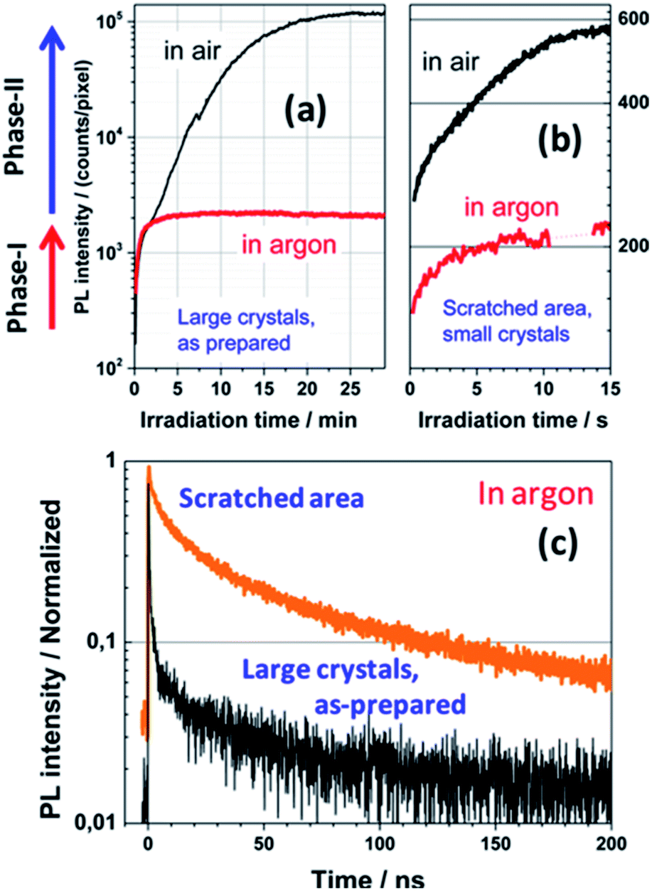 | ||
| Fig. 20 PL enhancement of large (a) and small (b) perovskite crystals in ambient air and in argon (λex = 514 nm, 1 W cm−2). Phase I: enhancement due to consumption of the oxygen dissolved in the material (identical in air and in argon). Phase II: further PL enhancement, which requires oxygen diffusion from the surface to the bulk (does not occur in argon). (c) Normalized PL kinetics measured in the as-prepared micrometer-sized crystals and scratched area (<100 nm grains) of the sample in argon (λex = 640 nm, repetition rate 2.5 MHz, 0.1 W cm−2, IRF width ≈ 100 ps). Reproduced with permission from ref. 189. Copyright 2015, American Chemical Society. | ||
Oxygen can decrease the deep defect states in perovskite materials, not only under illumination but also by thermal treatment in air.191,192 Oxygen acts as a p-type dopant in MAPbl3 in order to produce oxygen passivation.193 Oxygen diffusion can also induce fast degradation of perovskite thin films, similar to the “double-edged sword” effect of Pbl2 passivation at the perovskite grain boundaries.194 By the formation of superoxide (O2−) species, which accelerate the decomposition of perovskite materials, the speed of diffusion of oxygen into the MAPbl3 film increases. The photo-induced formation of superoxide species from O2 can be mitigated by thin-film passivation with iodide salts, which results in higher stability.195 Consequently, this approach has been successfully applied to fabricate highly efficient and stable PSCs (PCE of 22.1%).5
Carnie et al. investigated the effects of addition of 3-aminopropyl (3-oxobutanoic acid)-functionalized silica nanoparticles (f-SiO2) to the perovskite precursor solution on the photovoltaic performance of the resulting PSCs. Modification with f-SiO2 enhanced the performance of MAPbI3−xClx PSCs due to decreases in the number and size of pinholes in the perovskite film during processing.196
4.8. Passivation of perovskite films using 2D perovskite
Recently, two-dimensional (2D) perovskites have been proposed as passivation layers between the 3D perovskite and HTL interface due to their better stability than 3D perovskite and great potential in grain boundary passivation, bulk passivation and surface defect passivation of 3D perovskites.197–202 The deposition of a bulky organic cation on a pre-formed 3D perovskite surface induces in situ growth of a 2D perovskite layer through a reaction with excess PbI2. This approach improves the stability and photovoltaic performance due to the decreased number of surface trap states and suppressed interfacial charge recombination by the favorable band alignment of the 3D/2D mixed-layered structure.Cho et al. developed a procedure for the direct growth of a low-dimensional perovskite layer of (PEA)2PbI4 (PEA = phenylethylammonium) on top of the 3D perovskite surface, which leads to improved thermal stability of the devices and increases the PCE to 20.75%.200 Top view scanning electron microscopy (SEM) analysis showed that the perovskite film with a 2D perovskite layer has a smoother and more homogeneous morphology and decreased grain boundaries compared to the pristine perovskite film. In other related work, the treatment of a carbon electrode with PEAI resulted in the formation of a 2D perovskite at the interface between the perovskite and carbon layers (Fig. 21a and b).203 The interfacial growth of the ultrathin PEA2PbI4 layer provided better band energy alignment with favorable hole transport and higher conduction levels to block electron flow, which greatly suppressed the interfacial charge recombination (Fig. 21c). The PEA-modified devices showed greatly improved stability over 1000 h of exposure to ambient conditions. In a similar manner, a fluorinated aromatic ammonium cation, 2-(4-fluorophenyl)ethyl ammonium iodide (FPEAI), was introduced to in situ grow a 2D perovskite layer on top of a Cs/FA/MA triple-cation 3D perovskite film in a reaction with excess PbI2.204 The resulting FPEA2PbI4 perovskite layer acts as an efficient capping layer to protect the 3D perovskite from moisture; it also simultaneously decreases the charge recombination and promotes hole transportation at the perovskite/HTL interface.
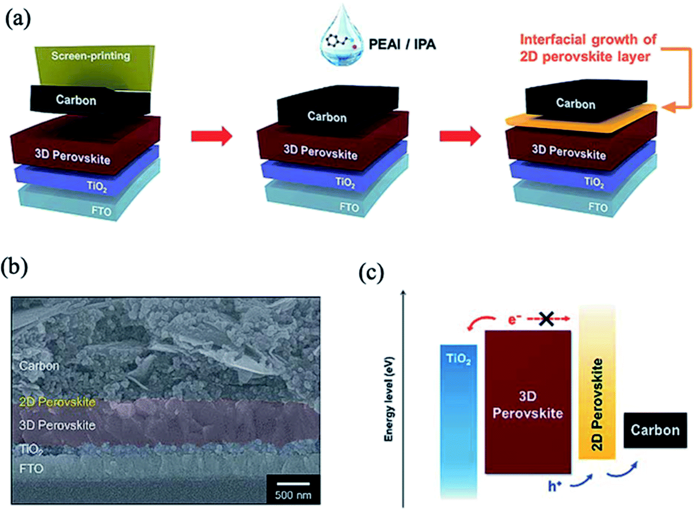 | ||
| Fig. 21 (a) Schematic showing the procedures to deposit a carbon electrode and induce interfacial growth of a 2D perovskite layer. (b) Cross-sectional field emission-scanning electron microscopy (FE-SEM) image of the fabricated PSC. (c) Energy band diagram of each component in the fabricated PSC showing the separation and transport of photo-generated carriers. Reprinted with permission from ref. 203. Copyright 2018 Royal Society of Chemistry. | ||
Luo et al. demonstrated a solution-processed secondary growth strategy (SSG) to produce a wider bandgap layer on top of n-type 3D perovskite films with the assistance of guanidinium bromide. This procedure improved the perovskite film quality and decreased the nonradiative recombination in the inverted PSCs, leading to a stabilized power output approaching 21% and long-term stability.205 Recently, n-hexyl trimethyl ammonium bromide was used for the formation of a thin layer of wide-bandgap halide (WBH) perovskite on top of a narrow-bandgap light-absorbing layer.206 The WBH layer effectively decreased recombination at the perovskite/P3HT interface through favourable van der Waals interactions. Based on this approach, the modified device showed a certified PCE of 22.7% and high stability at 85% relative humidity without encapsulation.
4.9. Passivation of perovskite films using quantum dots
The main issue that hinders the commercialization of PSCs is the instability of their performance under humidity, light exposure and high temperature. It was found that the stability and performance of PSCs can be enhanced using lead halide perovskite quantum dots (QDs), which passivate the GBs and enhance the crystallinity of the perovskite absorber layer.207–210 Moreover, lead halide perovskite QDs appear to be promising additives for interface engineering to control the perovskite band structure due to their high photoluminescence quantum yields and tunable energy bands.Cha et al. developed a method to tune the photovoltaic performance of PSCs by incorporating MAPbBr3−xIx QDs between the MAPbI3 perovskite film and the HTM layer (Fig. 22a).211 By adjustment of the Br:I ratio, the MAPbBr3−xIx QDs showed tunable fluorescence and band energy levels, as shown in Fig. 22b. The interfacial modification with the MAPbBr0.9I2.1 QDs provided appropriate band energy alignment; this facilitates the hole extraction, which enhances the charge carrier lifetime and, hence, the photovoltaic performance. However, the poor chemical stability of MAPbBr3−xIx QDs is regarded as the main obstacle that limits their application in PSCs. Thus, all-inorganic cesium-based perovskite QDs were used as effective additives to modify the perovskite/HTM interface. For example, Akin et al. implemented an interfacial layer of CsPbBr1.85I1.15 QDs between triple-cation based perovskite and spiro-OMeTAD layers in PSCs.212 This modification shields the perovskite layer from moisture and ion migration as well as light exposure and thus improves the stability of the cells. Moreover, CsPbBr1.85I1.15 QDs increased the ability of hole transport by pulling out holes from the inner perovskite layer and decreased the charge recombination by preventing back flow of electrons (Fig. 22c). A maximum PCE as high as 21.14% was achieved, along with long term stability (Fig. 22d). In a similar manner, CsPbBr3 QDs were introduced between the perovskite/HTL interface to improve the morphology and crystallinity of MAPbI3 films.213 The introduction of a proper amount of CsPbBr3 QDs led to the crystallization of a passivation layer of Cs1−yMAyPbI3−xBrx on top of the perovskite layer with fewer grain boundaries and lower defect density; this facilitates the charge extraction and transport at the interfaces. Recently, CsPbBrCl2 QDs were applied as surface modifiers for improving both the PCE and stability of MAPbI3 solar cells.208 The long hydrophobic alkane tails from the perovskite QD ligands were self-assembled on the MAPbI3 surface and retarded the moisture permeation by blocking the escape of MA cations (Fig. 22e). In turn, the QD elemental dopants were uniformly distributed across the MAPbI3 film and passivated the defect trap states. As a result, a CsPbBrCl2 QDs-based device yielded PCEs up to 21.5% and maintained 80% of the initial PCE after 500 h of continuous illumination.
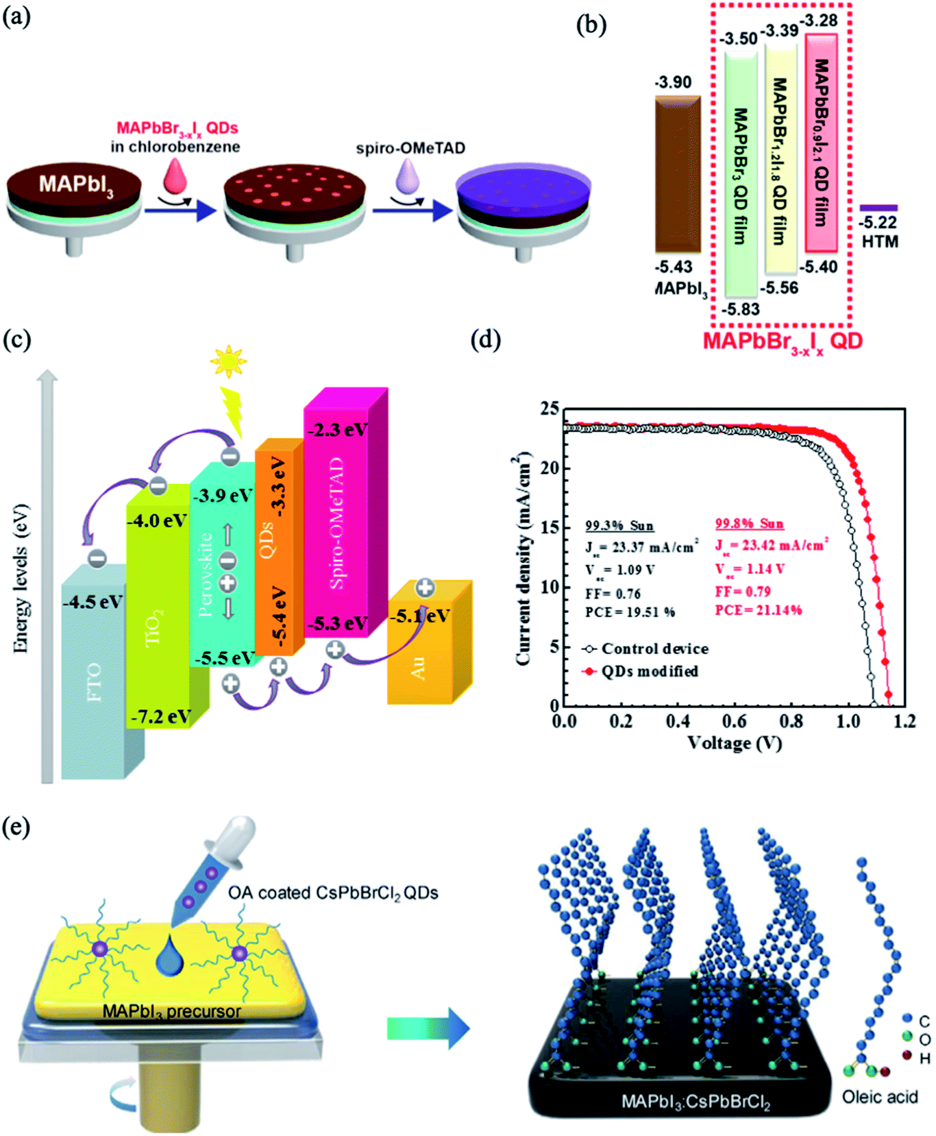 | ||
| Fig. 22 (a) Schematic of the fabrication procedures of perovskite solar cells with MAPbBr3−xIx QDs. (b) Energy diagram of each material in the MAPbBr3−xIx QDs-modified devices. Reproduced with permission from ref. 211. Copyright 2016, American Chemical Society. (c) Energy diagram of each material in the CsPbBr1.85I1.15 QDs-modified device. (d) J–V curves for the optimal CsPbBr1.85I1.15 QDs-modified device. Reprinted with permission from ref. 212. Copyright 2019 Elsevier. (e) Schematic of the procedure for preparing MAPbI3 films using CsPbBrCl2QDs. Reprinted with permission from ref. 208. Copyright 2019 Elsevier. | ||
In addition to lead halide perovskite QDs, carbon quantum dots (CQDs) have emerged as efficient additives for perovskite absorbers to improve the PCE and the stability of PSC devices.207 The authors demonstrated that the hydroxyl and carbonyl functional groups present on CDQs passivated the uncoordinated Pb2+ ions in the GBs and decreased the nonradiative recombination in the perovskite layer, leading to the formation of perovskite films with higher photoluminescence intensities and longer carrier lifetimes. The best CDQs-modified device achieved a PCE of 18.24% and retained 73.4% of this value after being aged for 48 h under 80% humidity in the dark at room temperature.
5. Passivation at the HTL and top electrode interface
The conventionally used Ag and Au electrodes may cause degradation of PSCs by diffusing through the HTM layer and perovskite layer.214 The use of different electrodes based on carbon or other metals and deposition of an interfacial layer to block metal migration can enable the fabrication of stable PSCs.215 Sanehira et al. studied different electrodes (Au, Ag, MoOx/Au, MoOx/Ag, and MoOx/Al) in PSCs and found that the most stable device was composed of MoOx/Al due to its spontaneous formation of an ultra-thin aluminum oxide layer, which inhibits decomposition of the perovskite films under illumination.216 Other work demonstrated that by adding a thin layer of Ni to the Au electrode in CH3NH3PbI3-based PSCs, better photocurrent stability and water stability can be obtained because the Ni layer functions as a hole-transfer catalyst and a physical passivation barrier.217,218 Improvement of the quality of the HTL was also achieved by modification of its surface with a thin layer of rubrene.219 This interfacial modification enhanced the carrier extraction and charge transfer, leading to a device with a high PCE of 19.87% and negligible hysteresis. Moreover, the introduction of rubrene improved the stability of the devices in a humid environment due to its lower water wettability.6. Conclusion and outlook
Among next-generation photovoltaic technologies, PSCs have drawn special attention from the research community due to their incredible power conversion efficiency, lower cost and ease of fabrication. According to a recent NREL PV chart, the best PSC has already achieved a PCE of 25.2%. However, the most efficient PSCs are based on lead (Pb) cation, which is toxic in nature. Other issues, such as instability due to humidity, light exposure, and high temperature, and the dependency of the J–V hysteresis curves restricts the commercialization of PSCs. The interfacial inhomogeneity of the heterostructure layers produces various trap states and large numbers of grain boundaries, which are the main cause of the instability of PSCs. Developing reliable and reproducible methods to produce highly efficient and stable devices that can compete with conventional silicon cells for the enormous PV market remains a challenging task.Our review summarizes the effects of additive engineering of the interfaces in addition to different layers in terms of chemical passivation, including the opto-electronic role of additives, band alignment and interface engineering. Changes in the work function can be induced by deposition of nonconjugated polymers on the transparent conductive oxide, which increases the charge collection and value of the Jsc. However, the influence of the TOC/ETL interface structures on the photovoltaic performance has not been paid as much attention as that on other device interfaces. The insertion of a monolayer with the ability of passivating surface defects on both the ETL and perovskite layer is regarded as a promising approach to improve the device efficiency and stability and decrease their I–V hysteresis phenomenon. The aim of introducing a thin buffer layer at the ETL/perovskite interface is to accelerate the electron injection and inhibit the interface recombination. Careful engineering of the interface is needed to minimize electron losses and to provide a correctly matched energy band alignment. Modification with metal/non-metal ions, fullerene and graphene-based materials, and organic and inorganic self-assembled monolayers results in better carrier transport and low charge recombination at the ETL/perovskite interface. Among these materials, the molecular design of C60 SAM derivatives with low solubility in polar solvents is a promising method to modify the optoelectronic properties of ETL and subsequently improve the efficiency of PSCs as well as decrease their I–V hysteresis. Further progress in the interfacial modification of the ETL surface should pave the way to design highly efficient charge transporting layers for the development of highly efficient PSCs.
The density of the GBs and the morphology of perovskite films have critical impacts on the photovoltaic performance and stability of PSCs; these can be controlled by passivation with additives such as thiocyanate, Cl/Br halide, PbI2, MAI, quantum dots and other organic molecules. The use of excess PbI2 or MAI and chloride additives (MACl, FACl) was demonstrated to be an effective method to passivate the grain boundaries of perovskite films and form large grains, respectively. Control of the hole injection from perovskite to HTL can be drastically improved by applying a passivation layer of hydrophobic groups and low-dimensional 2D perovskites or Lewis bases. The introduction of hydrophobic 2D perovskite on top of a 3D perovskite surface has emerged as a standard route to optimize perovskite for long term stability while maintaining high efficiency and will contribute to the realization of commercial PSCs. Thus, searching for new 2D layered perovskite compositions is highly attractive for offering better solutions to the current challenges in the perovskite research community. We also believe that Lewis base passivation strategies deserve further investigation because decreased defect densities as well as enhanced electronic properties are critical for improvement of PSC performance. On the other hand, modification of the HTL/top electrode interface improves the alignment of the band energy position and yields PSCs that are more stable against humidity. Further evolution of the HTL/metal electrode interface may provide a key for understanding the long-term stability of PSCs.
In-depth understanding of the relationship between the physicochemical properties of used additives and the improved properties of perovskite films is crucial for developing new additive systems. We expect that even greater performance enhancement can be achieved through further rational design of processing additives for interface engineering.
Conflicts of interest
We declare that there is no conflict of interest.Acknowledgements
M. M. T. would like to acknowledge the research laboratory of electronics (RLE) at Massachusetts Institute of Technology. D. P. acknowledges the financial support from the HOMING programme of the Foundation for Polish Science co-financed by the European Union under the European Regional Development Fund (POIR.04.04.00-00-5EE7/18-00).References
- A. K. Jena, A. Kulkarni and T. Miyasaka, Chem. Rev., 2019, 119, 3036–3103 CrossRef CAS PubMed
.
-
A. Kojima, K. TeshimaY. Shirai, T. Miyasaka, A. Kojima, K. Teshima, Y. Shirai and T. Miyasaka, in 212th ECS Meeting, 2008, p. 352 Search PubMed
- A. Kojima, K. Teshima, Y. Shirai and T. Miyasaka, J. Am. Chem. Soc., 2009, 131, 6050–6051 CrossRef CAS PubMed
- H.-S. Kim, C.-R. Lee, J.-H. Im, K.-B. Lee, T. Moehl, A. Marchioro, S.-J. Moon, R. Humphry-Baker, J.-H. Yum, J. E. Moser, M. Grätzel and N.-G. Park, Sci. Rep., 2012, 2, 591 CrossRef PubMed
- W. S. Yang, B.-W. Park, E. H. Jung, N. J. Jeon, Y. C. Kim, D. U. Lee, S. S. Shin, J. Seo, E. K. Kim, J. H. Noh and S. I. Seok, Science, 2017, 356, 1376–1379 CrossRef CAS PubMed
- N. J. Jeon, H. Na, E. H. Jung, T.-Y. Yang, Y. G. Lee, G. Kim, H.-W. Shin, S. Il Seok, J. Lee and J. Seo, Nat. Energy, 2018, 3, 682–689 CrossRef CAS
- https://www.nrel.gov/pv/cell-efficiency.html .
- Q. Zhang, M. M. Tavakoli, L. Gu, D. Zhang, L. Tang, Y. Gao, J. Guo, Y. Lin, S. F. Leung, S. Poddar, Y. Fu and Z. Fan, Nat. Commun., 2019, 10, 727 CrossRef
- M. Yavari, M. Mazloum-Ardakani, S. Gholipour, M. M. Tavakoli, S. H. Turren-Cruz, N. Taghavinia, M. Grätzel, A. Hagfeldt and M. Saliba, Adv. Energy Mater., 2018, 8, 1800177 CrossRef
- D. Prochowicz, R. Runjhun, M. M. Tavakoli, P. Yadav, M. Saski, A. Q. Alanazi, D. J. Kubicki, Z. Kaszkur, S. M. Zakeeruddin, J. Lewiński and M. Grätzel, Chem. Mater., 2019, 31, 1620–1627 CrossRef CAS
- M. M. Tavakoli, K. H. Tsui, Q. Zhang, J. He, Y. Yao, D. Li and Z. Fan, ACS Nano, 2015, 9, 10287–10295 CrossRef CAS
- Z. Zhao, F. Gu, H. Rao, S. Ye, Z. Liu, Z. Bian and C. Huang, Adv. Energy Mater., 2019, 9, 1802671 CrossRef
- M. M. Tavakoli, S. M. Zakeeruddin, M. Grätzel and Z. Fan, Adv. Mater., 2018, 30, 1705998 CrossRef
- Z. Xiao, Z. Song and Y. Yan, Adv. Mater., 2019, 1803792 CrossRef CAS
- Y. Zhou and Y. Zhao, Energy Environ. Sci., 2019, 12, 1495–1511 RSC
- M. Saliba, T. Matsui, J.-Y. Seo, K. Domanski, J.-P. Correa-Baena, M. K. Nazeeruddin, S. M. Zakeeruddin, W. Tress, A. Abate, A. Hagfeldt and M. Grätzel, Energy Environ. Sci., 2016, 9, 1989–1997 RSC
- Z. Yang, C.-C. Chueh, P.-W. Liang, M. Crump, F. Lin, Z. Zhu and A. K.-Y. Jen, Nano Energy, 2016, 22, 328–337 CrossRef CAS
- M. M. Tavakoli, P. Yadav, R. Tavakoli and J. Kong, Adv. Energy Mater., 2018, 1800794 CrossRef
- M. M. Tavakoli, W. Tress, J. V. Milić, D. Kubicki, L. Emsley and M. Grätzel, Energy Environ. Sci., 2018, 11, 3310–3320 RSC
- A. Waleed, M. M. Tavakoli, L. Gu, Z. Wang, D. Zhang, A. Manikandan, Q. Zhang, R. Zhang, Y. L. Chueh and Z. Fan, Nano Lett., 2016, 17, 523–530 CrossRef
- M. He, X. Pang, X. Liu, B. Jiang, Y. He, H. Snaith and Z. Lin, Angew. Chem., Int. Ed., 2016, 55, 4280–4284 CrossRef CAS
- K. O. Brinkmann, J. Zhao, N. Pourdavoud, T. Becker, T. Hu, S. Olthof, K. Meerholz, L. Hoffmann, T. Gahlmann, R. Heiderhoff, M. F. Oszajca, N. A. Luechinger, D. Rogalla, Y. Chen, B. Cheng and T. Riedl, Nat. Commun., 2017, 8, 13938 CrossRef CAS
- M. M. Tavakoli, A. Waleed, L. Gu, D. Zhang, R. Tavakoli, B. Lei, W. Su, F. Fang and Z. Fan, Nanoscale, 2017, 9, 5828–5834 RSC
- M. He, D. Zheng, M. Wang, C. Lin and Z. Lin, J. Mater. Chem. A, 2014, 2, 5994–6003 RSC
- M. M. Tavakoli, D. Bi, L. Pan, A. Hagfeldt, S. M. Zakeeruddin and M. Grätzel, Adv. Energy Mater., 2018, 8, 1800275 CrossRef
- M. Ye, C. He, J. Iocozzia, X. Liu, X. Cui, X. Meng, M. Rager, X. Hong, X. Liu and Z. Lin, J. Phys. D: Appl. Phys., 2017, 50, 373002 CrossRef
- Z. Zhao, F. Gu, H. Rao, S. Ye, Z. Liu, Z. Bian and C. Huang, Adv. Energy Mater., 2019, 9, 1802671 CrossRef
- J. Kim, A. Ho-Baillie and S. Huang, Sol. RRL, 2019, 3, 1800302 CrossRef
-
A. D. McNaught, A. Wilkinson and International Union of Pure and Applied Chemistry, Compendium of chemical terminology: IUPAC recommendations, Blackwell Science, 1997 Search PubMed
- J. Song, E. Zheng, J. Bian, X.-F. Wang, W. Tian, Y. Sanehira and T. Miyasaka, J. Mater. Chem. A, 2015, 3, 10837–10844 RSC
- D. Prochowicz, M. M. Tavakoli, S. H. Turren-Cruz, K. Pandey, M. Saliba and P. Yadav, Sustainable Energy Fuels, 2018, 2, 2407–2411 RSC
- J. Zhao, R. Tavakoli and M. M. Tavakoli, Chem. Commun., 2019, 55, 9196–9199 RSC
- D. Prochowicz, M. M. Tavakoli, A. Kalam, R. D. Chavan, S. Trivedi, M. Kumar and P. Yadav, J. Mater. Chem. A, 2019, 7, 8218–8225 RSC
- M. Yavari, M. Mazloum-Ardakani, S. Gholipour, M. M. Tavakoli, N. Taghavinia, A. Hagfeldt and W. Tress, ACS Omega, 2018, 3, 5038–5043 CrossRef CAS PubMed
- M. M. Tavakoli, A. Simchi, Z. Fan and H. Aashuri, Chem. Commun., 2016, 52, 323–326 RSC
- A. Tayyebi, M. M. Tavakoli, M. Outokesh, A. Shafiekhani and A. Simchi, Ind. Eng. Chem. Res., 2015, 54, 7382–7392 CrossRef CAS
- J. T. W. Wang, J. M. Ball, E. M. Barea, A. Abate, J. A. Alexander-Webber, J. Huang, M. Saliba, I. Mora-Sero, J. Bisquert, H. J. Snaith and R. J. Nicholas, Nano Lett., 2014, 14, 724–730 CrossRef CAS PubMed
- Y. Zhou, C. Fuentes-Hernandez, J. Shim, J. Meyer, A. J. Giordano, H. Li, P. Winget, T. Papadopoulos, H. Cheun, J. Kim, M. Fenoll, A. Dindar, W. Haske, E. Najafabadi, T. M. Khan, H. Sojoudi, S. Barlow, S. Graham, J.-L. Bredas, S. R. Marder, A. Kahn and B. Kippelen, Science, 2012, 336, 327–332 CrossRef CAS PubMed
- H. Zhou, Q. Chen, G. Li, S. Luo, T.-b. Song, H.-S. Duan, Z. Hong, J. You, Y. Liu and Y. Yang, Science, 2014, 345, 542–546 CrossRef CAS
- M. M. Tavakoli, D. Prochowicz, P. Yadav, R. Tavakoli and M. Saliba, Eng. Sci., 2018, 3, 48–53 Search PubMed
- P. Yadav, S. H. Turren-Cruz, D. Prochowicz, M. M. Tavakoli, K. Pandey, S. M. Zakeeruddin, M. Grätzel, A. Hagfeldt and M. Saliba, J. Phys. Chem. C, 2018, 122, 15149–15154 CrossRef CAS
- M. M. Tavakoli, F. Giordano, S. M. Zakeeruddin and M. Grätzel, Nano Lett., 2018, 18, 2428–2434 CrossRef CAS PubMed
- S. S. Mali, C. S. Shim, H. K. Park, J. Heo, P. S. Patil and C. K. Hong, Chem. Mater., 2015, 27, 1541–1551 CrossRef CAS
- M. Abdi-Jalebi, M. I. Dar, A. Sadhanala, S. P. Senanayak, M. Grätzel and R. H. Friend, J. Visualized Exp., 2017, 121, e55307 Search PubMed
- H. Zhou, Q. Chen, G. Li, S. Luo, T.-b. Song, H.-S. Duan, Z. Hong, J. You, Y. Liu and Y. Yang, Science, 2014, 345, 542–546 CrossRef CAS
- F. Giordano, A. Abate, J. P. Correa Baena, M. Saliba, T. Matsui, S. H. Im, S. M. Zakeeruddin, M. K. Nazeeruddin, A. Hagfeldt and M. Graetzel, Nat. Commun., 2016, 7, 10379 CrossRef CAS
- Z. Xu, X. Yin, Y. Guo, Y. Pu and M. He, J. Mater. Chem. C, 2018, 6, 4746–4752 RSC
- J. Wang, M. Qin, H. Tao, W. Ke, Z. Chen, J. Wan, P. Qin, L. Xiong, H. Lei, H. Yu and G. Fang, Appl. Phys. Lett., 2015, 106, 121104 CrossRef
- B. Roose, K. C. Gödel, S. Pathak, A. Sadhanala, J. P. C. Baena, B. D. Wilts, H. J. Snaith, U. Wiesner, M. Grätzel, U. Steiner and A. Abate, Adv. Energy Mater., 2016, 6, 1501868 CrossRef
- X.-X. Gao, Q.-Q. Ge, D.-J. Xue, J. Ding, J.-Y. Ma, Y.-X. Chen, B. Zhang, Y. Feng, L.-J. Wan and J.-S. Hu, Nanoscale, 2016, 8, 16881–16885 RSC
- Z. Ren, J. Wu, N. Wang and X. Li, J. Mater. Chem. A, 2018, 6, 15348–15358 RSC
- H. Tan, A. Jain, O. Voznyy, X. Lan, F. P. García de Arquer, J. Z. Fan, R. Quintero-Bermudez, M. Yuan, B. Zhang, Y. Zhao, F. Fan, P. Li, L. N. Quan, Y. Zhao, Z.-H. Lu, Z. Yang, S. Hoogland and E. H. Sargent, Science, 2017, 355, 722–726 CrossRef CAS
- T. Cao, Z. Wang, Y. Xia, B. Song, Y. Zhou, N. Chen and Y. Li, ACS Appl. Mater. Interfaces, 2016, 8, 18284–18291 CrossRef CAS
- B. L. Watson, N. Rolston, K. A. Bush, T. Leijtens, M. D. McGehee and R. H. Dauskardt, ACS Appl. Mater. Interfaces, 2016, 8, 25896–25904 CrossRef CAS
- A. Abrusci, S. D. Stranks, P. Docampo, H.-L. Yip, A. K.-Y. Jen and H. J. Snaith, Nano Lett., 2013, 13, 3124–3128 CrossRef CAS PubMed
- K. Wojciechowski, S. D. Stranks, A. Abate, G. Sadoughi, A. Sadhanala, N. Kopidakis, G. Rumbles, C.-Z. Li, R. H. Friend, A. K.-Y. Jen and H. J. Snaith, ACS Nano, 2014, 8, 12701–12709 CrossRef CAS
- S. Ryu, J. Seo, S. S. Shin, Y. C. Kim, N. J. Jeon, J. H. Noh and S. I. Seok, J. Mater. Chem. A, 2015, 3, 3271–3275 RSC
- J. Xie, X. Yu, J. Huang, X. Sun, Y. Zhang, Z. Yang, M. Lei, L. Xu, Z. Tang, C. Cui, P. Wang and D. Yang, Adv. Sci., 2017, 4, 1700018 CrossRef
- H.-R. Liu, S.-H. Li, L.-L. Deng, Z.-Y. Wang, Z. Xing, X. Rong, H.-R. Tian, X. Li, S.-Y. Xie, R.-B. Huang and L.-S. Zheng, ACS Appl. Mater. Interfaces, 2019, 11, 23982–23989 CrossRef CAS
- Y. Li, Y. Zhao, Q. Chen, Y. Yang, Y. Liu, Z. Hong, Z. Liu, Y.-T. Hsieh, L. Meng, Y. Li and Y. Yang, J. Am. Chem. Soc., 2015, 137, 15540–15547 CrossRef CAS PubMed
- M. M. Tavakoli, H. Aashuri, A. Simchi, S. Kalytchuk and Z. Fan, J. Phys. Chem. C, 2015, 119, 18886–18895 CrossRef CAS
- D. I. Son, B. W. Kwon, J. D. Yang, D. H. Park, W. S. Seo, H. Lee, Y. Yi, C. L. Lee and W. K. Choi, Nano Res., 2012, 5, 747–761 CrossRef CAS
- M. M. Tavakoli, A. Simchi and H. Aashuri, Mater. Chem. Phys., 2015, 156, 163–169 CrossRef CAS
- X. Meng, X. Cui, M. Rager, S. Zhang, Z. Wang, J. Yu, Y. W. Harn, Z. Kang, B. K. Wagner, Y. Liu, C. Yu, J. Qiu and Z. Lin, Nano Energy, 2018, 52, 123–133 CrossRef CAS
- Z. Zhu, J. Ma, Z. Wang, C. Mu, Z. Fan, L. Du, Y. Bai, L. Fan, H. Yan, D. L. Phillips and S. Yang, J. Am. Chem. Soc., 2014, 136, 3760–3763 CrossRef CAS PubMed
- M. M. Tavakoli, R. Tavakoli, P. Yadav and J. Kong, J. Mater. Chem. A, 2019, 7, 679–686 RSC
- M. M. Tavakoli, R. Tavakoli, Z. Nourbakhsh, A. Waleed, U. S. Virk and Z. Fan, Adv. Mater. Interfaces, 2016, 3, 1500790 CrossRef
- Y. Zhou, S. Yang, X. Yin, J. Han, M. Tai, X. Zhao, H. Chen, Y. Gu, N. Wang and H. Lin, J. Mater. Chem. A, 2019, 7, 1878–1888 RSC
- M. M. Tavakoli, R. Tavakoli, S. Hasanzadeh and M. H. Mirfasih, J. Phys. Chem. C, 2016, 120, 19531–19536 CrossRef CAS
- G. Yang, C. Wang, H. Lei, X. Zheng, P. Qin, L. Xiong, X. Zhao, Y. Yan and G. Fang, J. Mater. Chem. A, 2017, 5, 1658–1666 RSC
- K. Choi, H. Choi, J. Min, T. Kim, D. Kim, S. Y. Son, G.-W. Kim, J. Choi and T. Park, Sol. RRL, 2019, solr.201900251 CrossRef
- Y. Ogomi, A. Morita, S. Tsukamoto, T. Saitho, Q. Shen, T. Toyoda, K. Yoshino, S. S. Pandey, T. Ma and S. Hayase, J. Phys. Chem. C, 2014, 118, 16651–16659 CrossRef CAS
- L. Zuo, Q. Chen, N. De Marco, Y.-T. Hsieh, H. Chen, P. Sun, S.-Y. Chang, H. Zhao, S. Dong and Y. Yang, Nano Lett., 2017, 17, 269–275 CrossRef CAS PubMed
- L. F. Zhu, Y. Z. Xu, J. J. Shi, H. Y. Zhang, X. Xu, Y. H. Zhao, Y. H. Luo, Q. B. Meng and D. M. Li, RSC Adv., 2016, 6, 82282–82288 RSC
- M. Hou, H. Zhang, Z. Wang, Y. Xia, Y. Chen and W. Huang, ACS Appl. Mater. Interfaces, 2018, 10, 30607–30613 CrossRef CAS PubMed
- F. So and D. Kondakov, Adv. Mater., 2010, 22, 3762–3777 CrossRef CAS PubMed
- S. F. Shaikh, H.-C. Kwon, W. Yang, H. Hwang, H. Lee, E. Lee, S. Ma and J. Moon, J. Mater. Chem. A, 2016, 4, 15478–15485 RSC
- J. M. Marin-Beloqui, L. Lanzetta and E. Palomares, Chem. Mater., 2016, 28, 207–213 CrossRef CAS
- H.-W. Kang, J.-W. Lee, D.-Y. Son and N.-G. Park, RSC Adv., 2015, 5, 47334–47340 RSC
- G. S. Han, H. S. Chung, B. J. Kim, D. H. Kim, J. W. Lee, B. S. Swain, K. Mahmood, J. S. Yoo, N.-G. Park, J. H. Lee and H. S. Jung, J. Mater. Chem. A, 2015, 3, 9160–9164 RSC
- W. Li, W. Zhang, S. Van Reenen, R. J. Sutton, J. Fan, A. A. Haghighirad, M. B. Johnston, L. Wang and H. J. Snaith, Energy Environ. Sci., 2016, 9, 490–498 RSC
- M. M. Byranvand, T. Kim, S. Song, G. Kang, S. U. Ryu and T. Park, Adv. Energy Mater., 2018, 8, 1702235 CrossRef
- M. Liu, M. B. Johnston and H. J. Snaith, Nature, 2013, 501, 395–398 CrossRef CAS PubMed
- D. Prochowicz, M. M. Tavakoli, A. Solanki, T. W. Goh, K. Pandey, T. C. Sum, M. Saliba and P. Yadav, J. Mater. Chem. A, 2018, 6, 14307–14314 RSC
- M. M. Tavakoli, H. T. Dastjerdi, D. Prochowicz, P. Yadav, R. Tavakoli, M. Saliba and Z. Fan, J. Mater. Chem. A, 2019, 7, 14753–14760 RSC
- S. F. Leung, Q. Zhang, M. M. Tavakoli, J. He, X. Mo and Z. Fan, Small, 2016, 12, 2536–2548 CrossRef CAS PubMed
- W. E. I. Sha, X. Ren, L. Chen and W. C. H. Choy, Appl. Phys. Lett., 2015, 106, 221104 CrossRef
- C. Bi, Q. Wang, Y. Shao, Y. Yuan, Z. Xiao and J. Huang, Nat. Commun., 2015, 6, 7747 CrossRef CAS PubMed
- D. Prochowicz, P. Yadav, M. Saliba, D. J. Kubicki, M. M. Tavakoli, S. M. Zakeeruddin, J. Lewiński, L. Emsley and M. Grätzel, Nano Energy, 2018, 49, 523–528 CrossRef CAS
- M. M. Tavakoli, P. Yadav, D. Prochowicz, R. Tavakoli and M. Saliba, J. Phys. D: Appl. Phys., 2018, 52, 034005 CrossRef
- G. E. Eperon, V. M. Burlakov, P. Docampo, A. Goriely and H. J. Snaith, Adv. Funct. Mater., 2014, 24, 151–157 CrossRef CAS
- S. van Reenen, M. Kemerink and H. J. Snaith, J. Phys. Chem. Lett., 2015, 6, 3808–3814 CrossRef CAS PubMed
- M. M. Tavakoli, Q. Lin, S. F. Leung, G. C. Lui, H. Lu, L. Li, B. Xiang and Z. Fan, Nanoscale, 2016, 8, 4276–4283 RSC
- M. He, B. Li, X. Cui, B. Jiang, Y. He, Y. Chen, D. O'Neil, P. Szymanski, M. A. EI-Sayed, J. Huang and Z. Lin, Nat. Commun., 2017, 8, 16045 CrossRef CAS PubMed
- F. Huang, Y. Dkhissi, W. Huang, M. Xiao, I. Benesperi, S. Rubanov, Y. Zhu, X. Lin, L. Jiang, Y. Zhou, A. Gray-Weale, J. Etheridge, C. R. McNeill, R. A. Caruso, U. Bach, L. Spiccia and Y.-B. Cheng, Nano Energy, 2014, 10, 10–18 CrossRef CAS
- X. Li, D. Bi, C. Yi, J.-D. Decoppet, J. Luo, S. M. Zakeeruddin, A. Hagfeldt and M. Gratzel, Science, 2016, 353, 58–62 CrossRef CAS PubMed
- W. Nie, H. Tsai, R. Asadpour, J.-C. Blancon, A. J. Neukirch, G. Gupta, J. J. Crochet, M. Chhowalla, S. Tretiak, M. A. Alam, H.-L. Wang and A. D. Mohite, Science, 2015, 347, 522–525 CrossRef CAS PubMed
- Z. Xiao, Q. Dong, C. Bi, Y. Shao, Y. Yuan and J. Huang, Adv. Mater., 2014, 26, 6503–6509 CrossRef CAS PubMed
- C. Bi, Q. Wang, Y. Shao, Y. Yuan, Z. Xiao and J. Huang, Nat. Commun., 2015, 6, 7747 CrossRef CAS PubMed
- N. J. Jeon, J. H. Noh, Y. C. Kim, W. S. Yang, S. Ryu and S. Il Seok, Nat. Mater., 2014, 13, 897–903 CrossRef CAS PubMed
- Y. C. Kim, N. J. Jeon, J. H. Noh, W. S. Yang, J. Seo, J. S. Yun, A. Ho-Baillie, S. Huang, M. A. Green, J. Seidel, T. K. Ahn and S. Il Seok, Adv. Energy Mater., 2016, 6, 1502104 CrossRef
- M. Yang, Y. Zhou, Y. Zeng, C.-S. Jiang, N. P. Padture and K. Zhu, Adv. Mater., 2015, 27, 6363–6370 CrossRef CAS PubMed
- C. Bi, Q. Wang, Y. Shao, Y. Yuan, Z. Xiao and J. Huang, Nat. Commun., 2015, 6, 7747 CrossRef CAS PubMed
- J. Chen, P. J. Roland, R. J. Ellingson, C. Wang, Y. Yan, W. Liao, A. J. Cimaroli, N. Shrestha, C. R. Grice, Y. Yu and D. Zhao, ChemSusChem, 2016, 9, 3288–3297 CrossRef PubMed
- B. A. Koscher, J. K. Swabeck, N. D. Bronstein and A. P. Alivisatos, J. Am. Chem. Soc., 2017, 139, 6566–6569 CrossRef CAS PubMed
- B. Walker, G. Kim and J. Y. Kim, Adv. Mater., 2019, 31, 1807029 CrossRef PubMed
- Q. Jiang, D. Rebollar, J. Gong, E. L. Piacentino, C. Zheng and T. Xu, Angew. Chem., Int. Ed., 2015, 54, 7617–7620 CrossRef CAS PubMed
- Y. Chen, B. Li, W. Huang, D. Gao and Z. Liang, Chem. Commun., 2015, 51, 11997–11999 RSC
- M. Daub and H. Hillebrecht, Angew. Chem., Int. Ed., 2015, 54, 11016–11017 CrossRef CAS PubMed
- A. M. Ganose, C. N. Savory and D. O. Scanlon, J. Phys. Chem. Lett., 2015, 6, 4594–4598 CrossRef CAS PubMed
- Z. Xiao, W. Meng, B. Saparov, H.-S. Duan, C. Wang, C. Feng, W. Liao, W. Ke, D. Zhao, J. Wang, D. B. Mitzi and Y. Yan, J. Phys. Chem. Lett., 2016, 7, 1213–1218 CrossRef CAS PubMed
- W. Ke, C. Xiao, C. Wang, B. Saparov, H.-S. Duan, D. Zhao, Z. Xiao, P. Schulz, S. P. Harvey, W. Liao, W. Meng, Y. Yu, A. J. Cimaroli, C.-S. Jiang, K. Zhu, M. Al-Jassim, G. Fang, D. B. Mitzi and Y. Yan, Adv. Mater., 2016, 28, 5214–5221 CrossRef CAS PubMed
- M. K. Kim, T. Jeon, H. I. Park, J. M. Lee, S. A. Nam and S. O. Kim, CrystEngComm, 2016, 18, 6090–6095 RSC
- Y.-H. Chiang, M.-H. Li, H.-M. Cheng, P.-S. Shen and P. Chen, ACS Appl. Mater. Interfaces, 2017, 9, 2403–2409 CrossRef CAS PubMed
- Y. Yu, C. Wang, C. R. Grice, N. Shrestha, D. Zhao, W. Liao, L. Guan, R. A. Awni, W. Meng, A. J. Cimaroli, K. Zhu, R. J. Ellingson and Y. Yan, ACS Energy Lett., 2017, 2, 1177–1182 CrossRef CAS
- Y. Sun, J. Peng, Y. Chen, Y. Yao and Z. Liang, Sci. Rep., 2017, 7, 46193 CrossRef CAS PubMed
- W. Zhao, Z. Yao, F. Yu, D. Yang and S. F. Liu, Adv. Sci., 2018, 5, 1700131 CrossRef PubMed
- P. Zhao, W. Yin, M. Kim, M. Han, Y. J. Song, T. K. Ahn and H. S. Jung, J. Mater. Chem. A, 2017, 5, 7905–7911 RSC
- T. Bu, X. Liu, Y. Zhou, J. Yi, X. Huang, L. Luo, J. Xiao, Z. Ku, Y. Peng, F. Huang, Y.-B. Cheng and J. Zhong, Energy Environ. Sci., 2017, 10, 2509–2515 RSC
- J. K. Nam, S. U. Chai, W. Cha, Y. J. Choi, W. Kim, M. S. Jung, J. Kwon, D. Kim and J. H. Park, Nano Lett., 2017, 17, 2028–2033 CrossRef CAS PubMed
- M. Abdi-Jalebi, Z. Andaji-Garmaroudi, A. J. Pearson, G. Divitini, S. Cacovich, B. Philippe, H. Rensmo, C. Ducati, R. H. Friend and S. D. Stranks, ACS Energy Lett., 2018, 2671–2678 CrossRef CAS PubMed
- M. Abdi-Jalebi, Z. Andaji-Garmaroudi, S. Cacovich, C. Stavrakas, B. Philippe, J. M. Richter, M. Alsari, E. P. Booker, E. M. Hutter, A. J. Pearson, S. Lilliu, T. J. Savenije, H. Rensmo, G. Divitini, C. Ducati, R. H. Friend and S. D. Stranks, Nature, 2018, 555, 497–501 CrossRef CAS PubMed
- R. Zhang, M. Li, Y. Huan, J. Xi, S. Zhang, X. Cheng, H. Wu, W. Peng, Z. Bai and X. Yan, Inorg. Chem. Front., 2019, 6, 434–442 RSC
- A. Baldan, J. Mater. Sci., 2002, 37, 2171–2202 CrossRef CAS
- M. Yang, T. Zhang, P. Schulz, Z. Li, G. Li, D. H. Kim, N. Guo, J. J. Berry, K. Zhu and Y. Zhao, Nat. Commun., 2016, 7, 12305 CrossRef CAS PubMed
- C. Roldán-Carmona, P. Gratia, I. Zimmermann, G. Grancini, P. Gao, M. Graetzel and M. K. Nazeeruddin, Energy Environ. Sci., 2015, 8, 3550–3556 RSC
- M. M. Tavakoli, A. Simchi, X. Mo and Z. Fan, Mater. Chem. Front., 2017, 1, 1520–1525 RSC
- D. Bi, W. Tress, M. I. Dar, P. Gao, J. Luo, C. Renevier, K. Schenk, A. Abate, F. Giordano, J.-P. Correa Baena, J.-D. Decoppet, S. M. Zakeeruddin, M. K. Nazeeruddin, M. Grätzel and A. Hagfeldt, Sci. Adv., 2016, 2, e1501170 CrossRef PubMed
- T. J. Jacobsson, J. P. Correa-Baena, E. Halvani Anaraki, B. Philippe, S. D. Stranks, M. E. F. Bouduban, W. Tress, K. Schenk, J. Teuscher, J. E. Moser, H. Rensmo and A. Hagfeldt, J. Am. Chem. Soc., 2016, 138, 10331–10343 CrossRef CAS PubMed
- W. Peng, B. Anand, L. Liu, S. Sampat, B. E. Bearden, A. V. Malko and Y. J. Chabal, Nanoscale, 2016, 8, 1627–1634 RSC
- M. L. Petrus, Y. Hu, D. Moia, P. Calado, A. M. A. Leguy, P. R. F. Barnes and P. Docampo, ChemSusChem, 2016, 9, 2699–2707 CrossRef CAS PubMed
- Y. Lei, L. Gu, W. He, Z. Jia, X. Yang, H. Jia and Z. Zheng, J. Mater. Chem. A, 2016, 4, 5474–5481 RSC
- Q. Chen, H. Zhou, T.-B. Song, S. Luo, Z. Hong, H.-S. Duan, L. Dou, Y. Liu and Y. Yang, Nano Lett., 2014, 14, 4158–4163 CrossRef CAS PubMed
- T. Supasai, N. Rujisamphan, K. Ullrich, A. Chemseddine and Th. Dittrich, Appl. Phys. Lett., 2013, 103, 183906 CrossRef
- L. Wang, C. McCleese, A. Kovalsky, Y. Zhao and C. Burda, J. Am. Chem. Soc., 2014, 136, 12205–12208 CrossRef CAS PubMed
- S. Wang, W. Dong, X. Fang, Q. Zhang, S. Zhou, Z. Deng, R. Tao, J. Shao, R. Xia, C. Song, L. Hu and J. Zhu, Nanoscale, 2016, 8, 6600–6608 RSC
- F. Liu, Q. Dong, M. K. Wong, A. B. Djurišić, A. Ng, Z. Ren, Q. Shen, C. Surya, W. K. Chan, J. Wang, A. M. C. Ng, C. Liao, H. Li, K. Shih, C. Wei, H. Su and J. Dai, Adv. Energy Mater., 2016, 6, 1502206 CrossRef
- F. Jiang, Y. Rong, H. Liu, T. Liu, L. Mao, W. Meng, F. Qin, Y. Jiang, B. Luo, S. Xiong, J. Tong, Y. Liu, Z. Li, H. Han and Y. Zhou, Adv. Funct. Mater., 2016, 26, 8119–8127 CrossRef CAS
- S. Wang, W. Dong, X. Fang, Q. Zhang, S. Zhou, Z. Deng, R. Tao, J. Shao, R. Xia, C. Song, L. Hu and J. Zhu, Nanoscale, 2016, 8, 6600–6608 RSC
- Y. Chen, B. Li, W. Huang, D. Gao and Z. Liang, Chem. Commun., 2015, 51, 11997–11999 RSC
- T. Zhang, N. Guo, G. Li, X. Qian and Y. Zhao, Nano Energy, 2016, 26, 50–56 CrossRef CAS
- Q. Chen, H. Zhou, T.-B. Song, S. Luo, Z. Hong, H.-S. Duan, L. Dou, Y. Liu and Y. Yang, Nano Lett., 2014, 14, 4158–4163 CrossRef CAS PubMed
- M. Moriya, D. Hirotani, T. Ohta, Y. Ogomi, Q. Shen, T. S. Ripolles, K. Yoshino, T. Toyoda, T. Minemoto and S. Hayase, ChemSusChem, 2016, 9, 2634–2639 CrossRef CAS PubMed
- C. Wang, D. Zhao, Y. Yu, N. Shrestha, C. R. Grice, W. Liao, A. J. Cimaroli, J. Chen, R. J. Ellingson, X. Zhao and Y. Yan, Nano Energy, 2017, 35, 223–232 CrossRef CAS
- D.-Y. Son, J.-W. Lee, Y. J. Choi, I.-H. Jang, S. Lee, P. J. Yoo, H. Shin, N. Ahn, M. Choi, D. Kim and N.-G. Park, Nat. Energy, 2016, 1, 16081 CrossRef CAS
- S. Ham, Y. J. Choi, J.-W. Lee, N.-G. Park and D. Kim, J. Phys. Chem. C, 2017, 121, 3143–3148 CrossRef CAS
- B. Hwang, C. Gu, D. Lee and J.-S. Lee, Sci. Rep., 2017, 7, 43794 CrossRef PubMed
- G. Chai, S. Luo, H. Zhou and W. A. Daoud, Mater. Des., 2017, 125, 222–229 CrossRef CAS
- N. Li, C. Shi, L. Li, Z. Zhang and C. Ma, Superlattices Microstruct., 2017, 104, 445–450 CrossRef CAS
- F. Zhang, B. Yang, X. Mao, R. Yang, L. Jiang, Y. Li, J. Xiong, Y. Yang, R. He, W. Deng and K. Han, ACS Appl. Mater. Interfaces, 2017, 9, 14827–14832 CrossRef CAS PubMed
- Q. Chen, H. Zhou, Y. Fang, A. Z. Stieg, T.-B. Song, H.-H. Wang, X. Xu, Y. Liu, S. Lu, J. You, P. Sun, J. McKay, M. S. Goorsky and Y. Yang, Nat. Commun., 2015, 6, 7269 CrossRef CAS PubMed
- F. Xu, T. Zhang, G. Li and Y. Zhao, ChemSusChem, 2017, 10, 2365–2369 CrossRef CAS PubMed
- Z. Li, C. Kolodziej, C. McCleese, L. Wang, A. Kovalsky, A. C. Samia, Y. Zhao and C. Burda, Nanoscale Adv., 2019, 1, 827–833 RSC
- M. M. Tavakoli, M. Saliba, P. Yadav, P. Holzhey, A. Hagfeldt, S. M. Zakeeruddin and M. Grätzel, Adv. Energy Mater., 2019, 9, 1802646 CrossRef
- M. M. Tavakoli, P. Yadav, D. Prochowicz, M. Sponseller, A. Osherov, V. Bulović and J. Kong, Adv. Energy Mater., 2019, 1803587 CrossRef
- N. De Marco, H. Zhou, Q. Chen, P. Sun, Z. Liu, L. Meng, E.-P. Yao, Y. Liu, A. Schiffer and Y. Yang, Nano Lett., 2016, 16, 1009–1016 CrossRef PubMed
- D. J. Kubicki, D. Prochowicz, A. Hofstetter, M. Saski, P. Yadav, D. Bi, N. Pellet, J. Lewiński, S. M. Zakeeruddin, M. Grätzel and L. Emsley, J. Am. Chem. Soc., 2018, 140, 3345–3351 CrossRef CAS PubMed
- Y. Wang, N. Song, L. Feng and X. Deng, ACS Appl. Mater. Interfaces, 2016, 8, 24703–24711 CrossRef CAS PubMed
- N. Li, C. Shi, L. Li, Z. Zhang and C. Ma, Superlattices Microstruct., 2017, 104, 445–450 CrossRef CAS
- M. Kim, B. J. Kim, D.-Y. Son, N.-G. Park, H. S. Jung and M. Choi, Nano Lett., 2016, 16, 5756–5763 CrossRef CAS PubMed
- G. Chai, S. Luo, H. Zhou and W. A. Daoud, Mater. Des., 2017, 125, 222–229 CrossRef CAS
- M. Ibrahim Dar, M. Abdi-Jalebi, N. Arora, T. Moehl, M. Grätzel and M. K. Nazeeruddin, Adv. Mater., 2015, 27, 7221–7228 CrossRef CAS PubMed
- F. Zhang, B. Yang, X. Mao, R. Yang, L. Jiang, Y. Li, J. Xiong, Y. Yang, R. He, W. Deng and K. Han, ACS Appl. Mater. Interfaces, 2017, 9, 14827–14832 CrossRef CAS PubMed
- C. M. Sutter-Fella, Y. Li, M. Amani, J. W. Ager, F. M. Toma, E. Yablonovitch, I. D. Sharp and A. Javey, Nano Lett., 2016, 16, 800–806 CrossRef CAS PubMed
- G. Y. Kim, S. H. Oh, B. P. Nguyen, W. Jo, B. J. Kim, D. G. Lee and H. S. Jung, J. Phys. Chem. Lett., 2015, 6, 2355–2362 CrossRef CAS PubMed
- F. Xu, T. Zhang, G. Li and Y. Zhao, ChemSusChem, 2017, 10, 2365–2369 CrossRef CAS PubMed
- T. Li, Y. Pan, Z. Wang, Y. Xia, Y. Chen and W. Huang, J. Mater. Chem. A, 2017, 5, 12602–12652 RSC
- Y. Li, L. Ji, R. Liu, C. Zhang, C. H. Mak, X. Zou, H.-H. Shen, S.-Y. Leu and H.-Y. Hsu, J. Mater. Chem. A, 2018, 6, 12842–12875 RSC
- P.-W. Liang, C.-Y. Liao, C.-C. Chueh, F. Zuo, S. T. Williams, X.-K. Xin, J. Lin and A. K.-Y. Jen, Adv. Mater., 2014, 26, 3748–3754 CrossRef CAS PubMed
- C.-C. Chueh, C.-Y. Liao, F. Zuo, S. T. Williams, P.-W. Liang and A. K.-Y. Jen, J. Mater. Chem. A, 2015, 3, 9058–9062 RSC
- L. Li, Y. Chen, Z. Liu, Q. Chen, X. Wang and H. Zhou, Adv. Mater., 2016, 28, 9862–9868 CrossRef CAS PubMed
- S. You, S. Bi, J. Huang, Q. Jia, Y. Yuan, Y. Xia, Z. Xiao, Z. Sun, J. Liu, S. Sun and Z. Zhao, Chem.–Eur. J., 2017, 23, 18140–18145 CrossRef CAS PubMed
- Y.-H. Kye, C.-J. Yu, U.-G. Jong, Y. Chen and A. Walsh, J. Phys. Chem. Lett., 2018, 9, 2196–2201 CrossRef CAS PubMed
- C.-G. Wu, C.-H. Chiang, Z.-L. Tseng, M. K. Nazeeruddin, A. Hagfeldt and M. Grätzel, Energy Environ. Sci., 2015, 8, 2725–2733 RSC
- C.-H. Chiang, M. K. Nazeeruddin, M. Grätzel and C.-G. Wu, Energy Environ. Sci., 2017, 10, 808–817 RSC
- X. Gong, M. Li, X.-B. Shi, H. Ma, Z.-K. Wang and L.-S. Liao, Adv. Funct. Mater., 2015, 25, 6671–6678 CrossRef CAS
- A. Abate, M. Saliba, D. J. Hollman, S. D. Stranks, K. Wojciechowski, R. Avolio, G. Grancini, A. Petrozza and H. J. Snaith, Nano Lett., 2014, 14, 3247–3254 CrossRef CAS PubMed
- N. K. Noel, A. Abate, S. D. Stranks, E. S. Parrott, V. M. Burlakov, A. Goriely and H. J. Snaith, ACS Nano, 2014, 8, 9815–9821 CrossRef CAS
- T. Y. Wen, S. Yang, P. F. Liu, L. J. Tang, H. W. Qiao, X. Chen, X. H. Yang, Y. Hou and H. G. Yang, Adv. Energy Mater., 2018, 8, 1703143 CrossRef
- Y. Lin, L. Shen, J. Dai, Y. Deng, Y. Wu, Y. Bai, X. Zheng, J. Wang, Y. Fang, H. Wei, W. Ma, X. C. Zeng, X. Zhan and J. Huang, Adv. Mater., 2017, 29, 1604545 CrossRef PubMed
- Y. Guo, J. Ma, H. Lei, F. Yao, B. Li, L. Xiong and G. Fang, J. Mater. Chem. A, 2018, 6, 5919–5925 RSC
- G. Yang, P. Qin, G. Fang and G. Li, Sol. RRL, 2018, 2, 1800055 CrossRef
- Q. Wang, Q. Dong, T. Li, A. Gruverman and J. Huang, Adv. Mater., 2016, 28, 6734–6739 CrossRef CAS PubMed
- I. Hwang, I. Jeong, J. Lee, M. J. Ko and K. Yong, ACS Appl. Mater. Interfaces, 2015, 7, 17330–17336 CrossRef CAS PubMed
- B. Chaudhary, A. Kulkarni, A. K. Jena, M. Ikegami, Y. Udagawa, H. Kunugita, K. Ema and T. Miyasaka, ChemSusChem, 2017, 10, 2473–2479 CrossRef CAS PubMed
- X. Huang, H. Guo, K. Wang and X. Liu, Org. Electron., 2017, 41, 42–48 CrossRef CAS
- L. Zuo, H. Guo, D. W. deQuilettes, S. Jariwala, N. De Marco, S. Dong, R. DeBlock, D. S. Ginger, B. Dunn, M. Wang and Y. Yang, Sci. Adv., 2017, 3, e1700106 CrossRef PubMed
- F. Wang, W. Geng, Y. Zhou, H. H. Fang, C. J. Tong, M. A. Loi, L. M. Liu and N. Zhao, Adv. Mater., 2016, 28, 9986–9992 CrossRef CAS PubMed
- Y. Tian, A. Merdasa, E. Unger, M. Abdellah, K. Zheng, S. McKibbin, A. Mikkelsen, T. Pullerits, A. Yartsev, V. Sundström and I. G. Scheblykin, J. Phys. Chem. Lett., 2015, 6, 4171–4177 CrossRef CAS PubMed
- Y. Tian, M. Peter, E. Unger, M. Abdellah, K. Zheng, T. Pullerits, A. Yartsev, V. Sundström and I. G. Scheblykin, Phys. Chem. Chem. Phys., 2015, 17, 24978–24987 RSC
- A. Ng, Z. Ren, Q. Shen, S. H. Cheung, H. C. Gokkaya, S. K. So, A. B. Djurišić, Y. Wan, X. Wu and C. Surya, ACS Appl. Mater. Interfaces, 2016, 8, 32805–32814 CrossRef CAS PubMed
- Z. Ren, A. Ng, Q. Shen, H. C. Gokkaya, J. Wang, L. Yang, W.-K. Yiu, G. Bai, A. B. Djurišić, W. W. Leung, J. Hao, W. K. Chan and C. Surya, Sci. Rep., 2015, 4, 6752 CrossRef PubMed
- W.-J. Yin, H. Chen, T. Shi, S.-H. Wei and Y. Yan, Adv. Electron. Mater., 2015, 1, 1500044 CrossRef
- T. J. Jacobsson, J.-P. Correa-Baena, E. Halvani Anaraki, B. Philippe, S. D. Stranks, M. E. F. Bouduban, W. Tress, K. Schenk, J. Teuscher, J.-E. Moser, H. Rensmo and A. Hagfeldt, J. Am. Chem. Soc., 2016, 138, 10331–10343 CrossRef CAS PubMed
- N. Aristidou, C. Eames, I. Sanchez-Molina, X. Bu, J. Kosco, M. S. Islam and S. A. Haque, Nat. Commun., 2017, 8, 15218 CrossRef PubMed
- M. J. Carnie, C. Charbonneau, M. L. Davies, B. O. Regan, D. A. Worsley and T. M. Watson, J. Mater. Chem. A, 2014, 2, 17077–17084 RSC
- H.-S. Yoo and N.-G. Park, Sol. Energy Mater. Sol. Cells, 2018, 179, 57–65 CrossRef CAS
- Y. Lin, Y. Bai, Y. Fang, Z. Chen, S. Yang, X. Zheng, S. Tang, Y. Liu, J. Zhao and J. Huang, J. Phys. Chem. Lett., 2018, 9, 654–658 CrossRef CAS
- N. Li, Z. Zhu, Q. Dong, J. Li, Z. Yang, C.-C. Chueh, A. K.-Y. Jen and L. Wang, Adv. Mater. Interfaces, 2017, 4, 1700598 CrossRef
- K. T. Cho, G. Grancini, Y. Lee, E. Oveisi, J. Ryu, O. Almora, M. Tschumi, P. A. Schouwink, G. Seo, S. Heo, J. Park, J. Jang, S. Paek, G. Garcia-Belmonte and M. K. Nazeeruddin, Energy Environ. Sci., 2018, 11, 952–959 RSC
- Y. Cho, A. M. Soufiani, J. S. Yun, J. Kim, D. S. Lee, J. Seidel, X. Deng, M. A. Green, S. Huang and A. W. Y. Ho-Baillie, Adv. Energy Mater., 2018, 8, 1703392 CrossRef
- P. Chen, Y. Bai, S. Wang, M. Lyu, J.-H. Yun and L. Wang, Adv. Funct. Mater., 2018, 28, 1706923 CrossRef
- K. Lee, J. Kim, H. Yu, J. W. Lee, C.-M. Yoon, S. K. Kim and J. Jang, J. Mater. Chem. A, 2018, 6, 24560–24568 RSC
- Q. Zhou, L. Liang, J. Hu, B. Cao, L. Yang, T. Wu, X. Li, B. Zhang and P. Gao, Adv. Energy Mater., 2019, 9, 1802595 CrossRef
- D. Luo, W. Yang, Z. Wang, A. Sadhanala, Q. Hu, R. Su, R. Shivanna, G. F. Trindade, J. F. Watts, Z. Xu, T. Liu, K. Chen, F. Ye, P. Wu, L. Zhao, J. Wu, Y. Tu, Y. Zhang, X. Yang, W. Zhang, R. H. Friend, Q. Gong, H. J. Snaith and R. Zhu, Science, 2018, 360, 1442–1446 CrossRef CAS PubMed
- E. H. Jung, N. J. Jeon, E. Y. Park, C. S. Moon, T. J. Shin, T.-Y. Yang, J. H. Noh and J. Seo, Nature, 2019, 567, 511–515 CrossRef CAS PubMed
- Y. Ma, H. Zhang, Y. Zhang, R. Hu, M. Jiang, R. Zhang, H. Lv, J. Tian, L. Chu, J. Zhang, Q. Xue, H. L. Yip, R. Xia, X. Li and W. Huang, ACS Appl. Mater. Interfaces, 2019, 11, 3044–3052 CrossRef CAS PubMed
- X. Zheng, J. Troughton, N. Gasparini, Y. Lin, M. Wei, Y. Hou, J. Liu, K. Song, Z. Chen, C. Yang, B. Turedi, A. Y. Alsalloum, J. Pan, J. Chen, A. A. Zhumekenov, T. D. Anthopoulos, Y. Han, D. Baran, O. F. Mohammed, E. H. Sargent and O. M. Bakr, Joule, 2019, 3, 1963–1976 CrossRef CAS
- Y. Wang, J. Zhang, S. Chen, H. Zhang, L. Li and Z. Fu, J. Mater. Sci., 2018, 53, 9180–9190 CrossRef CAS
- T. T. Ngo and I. Mora-Seró, J. Phys. Chem. Lett., 2019, 10, 1099–1108 CrossRef CAS PubMed
- M. Cha, P. Da, J. Wang, W. Wang, Z. Chen, F. Xiu, G. Zheng and Z.-S. Wang, J. Am. Chem. Soc., 2016, 138, 8581–8587 CrossRef CAS PubMed
- S. Akin, Y. Altintas, E. Mutlugun and S. Sonmezoglu, Nano Energy, 2019, 60, 557–566 CrossRef CAS
- Y. Gao, Y. Wu, H. Lu, C. Chen, Y. Liu, X. Bai, L. Yang, W. W. Yu, Q. Dai and Y. Zhang, Nano Energy, 2019, 59, 517–526 CrossRef CAS
- K. Domanski, J.-P. Correa-Baena, N. Mine, M. K. Nazeeruddin, A. Abate, M. Saliba, W. Tress, A. Hagfeldt and M. Grätzel, ACS Nano, 2016, 10, 6306–6314 CrossRef CAS PubMed
- B.-E. Cohen, M. Wierzbowska and L. Etgar, Sustainable Energy Fuels, 2017, 1, 1935–1943 RSC
- E. M. Sanehira, B. J. Tremolet de Villers, P. Schulz, M. O. Reese, S. Ferrere, K. Zhu, L. Y. Lin, J. J. Berry and J. M. Luther, ACS Energy Lett., 2016, 1, 38–45 CrossRef CAS
- C. Wang, S. Yang, X. Chen, T. Wen and H. G. Yang, J. Mater. Chem. A, 2017, 5, 910–913 RSC
- R. T. Ginting, M.-K. Jeon, K.-J. Lee, W.-Y. Jin, T.-W. Kim and J.-W. Kang, J. Mater. Chem. A, 2017, 5, 4527–4534 RSC
- M. M. Tavakoli, R. Tavakoli, D. Prochowicz, P. Yadav and M. Saliba, Mol. Syst. Des. Eng., 2018, 3, 717–722 RSC
Footnote |
| † These authors contributed equally to this work. |
| This journal is © The Royal Society of Chemistry 2020 |