Perceiving the temperature coefficients of carbon-based perovskite solar cells†
Received
22nd May 2020
, Accepted 16th October 2020
First published on 19th October 2020
Abstract
Perovskite solar cells (PSCs) have emerged in a “catfish effect” of other established photovoltaic technologies with the rapid development of high-power conversion efficiency (PCE) and low-cost fabrication. Among various kinds of PSCs, organic hole transport layer (HTL)-free carbon-based PSCs (c-PSCs) have been considered as the most promising devices due to their excellent stability. However, temperature becomes one of the crucial factors in determining the pace of PSC commercialization. Temperature stress at the interface between the perovskite film and the charge transport layer is an essential factor in determining the performance of c-PSCs. This work assesses the correlation between the temperature coefficient (TC) and different photovoltaic parameters for HTL-free c-PSCs. To evaluate different photovoltaic parameters of the c-PSC as a function of temperature, two different testing approaches namely under steady temperature (ST) and transient temperature (TT) conditions have been considered across a wide temperature window (5–75 °C) under 1 Sun 1.5 AM. Here TT testing involves subjecting a single c-PSC to a continuous temperature treatment, whereas ST testing consists of specific temperature treatment of an individual c-PSC. The maximum efficiency achieved at 25 °C for TT testing devices is ∼14.5%, which is ∼11% higher than that of ST testing devices (PCE ∼ 13%). Moreover, the efficiency temperature coefficient (ETC) for ST testing was found to be 3.5 × 10⁻² (5 °C ≤ T ≤ 25 °C) and −2.1 × 10⁻² (25 °C ≤ T ≤ 75 °C), whereas the ETC values of TT testing devices were +2.5 × 10⁻² (5 °C ≤ T ≤ 25 °C) and −1.8 × 10⁻² (25 °C ≤ T ≤ 75 °C), respectively. The outcome of temperature stress transmitting through different interfacial layers was further investigated by thermal imaging of TT devices. On the other hand, X-ray diffraction and scanning electron microscopy structural analyses were performed to understand the effect of thermal stress on the overall performance of ST devices. It has been observed that TC values obtained under TT testing conditions are reversible, whereas in the case of ST testing the TC values are irreversible which shows degradation of the device.
Introduction
Perovskite solar cells (PSCs) with their cutting-edge technology have been universally elevated as an economically and environmentally feasible renewable technology option in place of regular and traditional solar cell technologies for addressing the global challenges in the area of energy generation and climate change.1,2 From initial development to use of carbon as a counter electrode, extensive studies have been done in this field, and to date, the highest photo-conversion efficiency (PCE) achieved for PSCs has been 25.2%.3–19 Engineering of interfaces and grain boundary of the perovskite layer can further help to enrich the PSC field towards more stable, reliable and enhanced PCE generating devices. Despite this massive development, there are issues related to upscaling, toxicity, and stability of performance that restrict the commercialization of PSCs.2,20 Due to the cost-effectiveness, environmental superiority, abundance, and excellent photo-electrochemical catalytic activity, carbon plays critical roles in the charge transport layer, as well as the counter electrode utilizing different polymorphs like carbon nanotubes, fullerene, graphite, and graphene.21–23 Carbon polymorphs as charge transport materials produced the highest PCE of 21.1% whereas as electrode materials for hole-selective layer-free devices, they were able to provide the highest PCE of 16.26%.24,25 With the potential of achieving even higher efficiencies and very low production costs, c-PSCs have become commercially attractive.
However, temperature is one of the most crucial external factors that influence the photovoltaic performance and stability of PSCs. Temperature strongly influences physical parameters, like charge diffusion in the layers and/or recombination reactions of the generated electrons in the device.26 To date, studies on temperature-dependent c-PSCs are a limited and less-explored area of research compared with numerous studies on improving the PCE and stability of c-PSC devices. There are few studies on temperature-dependent PSCs, which suggest a maximum PCE around room temperature with successive performance curtailment under higher or lower temperature conditions.27–30 Most of the studies reveal the accumulation of ions at selective interfacial contacts during temperature stress. This further signifies evaporation of additives in the hole transport layer (HTL) as the reason behind such performance decline of a PSC device.31,32 In this regard, our study aims to investigate and understand the role of temperature coefficients (TC) of c-PSCs using photovoltaic parameters such as short circuit current (JSC), open-circuit voltage (VOC), fill factor (FF) and power conversion efficiency (PCE) in visualizing the commercialization of solar cells.33,34 The relative change of a temperature-dependent parameter corresponding to the change of temperature is known as the temperature coefficient of that parameter.35 The physics of temperature coefficients (TC) of solar cells suggests a strong dependency of VOC and JSC on temperature, as the balance between charge carrier generation and recombination can be affected by temperature.34 Also, the temperature dependency of bandgap shift plays a vital role along with the incident spectrum in affecting the cell parameters.36 Extensive research on performance variation with temperature to pin-point the temperature coefficient and deducing the origin of interfacial damage needs to be done for c-PSCs. It has been observed that for the three most widely commercialized thin-film solar cells namely α-Si, CdTe and copper indium gallium selenide, the TC values are negative.37,38 Although, they are highly effective in large scale operation. A negative TC value normally implies that with the increase of temperature, the parameter of interest will decrease, which can affect the performance of solar cells in a hot climate. Again a positive TC value indicates that the increase of temperature will increase the performance, which can impact the performance of the device in a cold climate.39 In contrast, reports on TC value evaluation are less explored for PSCs. The commercialization of PSCs highly depends on the TC values of the devices because PV cells in the ground are operated at lower or higher temperatures relative to standard test conditions (STC, the temperature is taken as 25 °C), depending on the environment, leading to changes in the average PCE, as reported for silicon solar cells.33,34,40–43 Under different climatic conditions, the yearly average temperature varies significantly from the STC.44 On the earth's surface, every location usually undergoes a daily (in 24 hours) temperature variation of ∼5 to 10 °C or sometimes more than that.45,46 In areas where the variation is ∼5 °C or less in 24 hours, it is possible that the performance of the devices can be different from places where the variation is 10 °C or more due to inherent properties of materials like specific heat capacities.47,48 A change of 10 °C can significantly vary the performance of PSC devices, and detection of TC values is inevitable in this scenario. This kind of temperature variation can disrupt the instantaneous thermal equilibrium between different materials depending on specific heat capacity and thermal conductivity.49
Therefore, in this work, steady temperature (ST) and transient temperature (TT) temperature conditions are introduced to understand their effect on the interface between the CH3NH3PbI3 perovskite film and the charge transport layer and on the performances of c-PSCs in the temperature range of 5 °C to 75 °C. Here ST and TT terms are designated depending on conditions of experimentation. Characterization of a particular device at different temperatures starting from 5 °C to 75 °C is termed as TT testing, which could be more realistic for everyday temperature variation of ≥10 °C on the earth's surface. On the other hand, keeping different devices at different temperatures (i.e. a particular device was kept at a particular temperature) in the 5 °C to 75 °C range for examination is called ST testing, which could be more realistic for everyday temperature variation ≤5 °C for a long time. Observations indicate a clear spectrum of TC values of different photovoltaic parameters for the first time, along with the probable reasons behind significant performance variations. This finding will be relevant for industrial applications in both single-junction and tandem architectures for c-PSC devices in future.
Results and discussion
Crystal growth via the solvent exchange method to develop c-PSCs
Crystal growth via the solvent exchange (CGSE) method turns out to be an effective one-step approach for the fabrication of organic hole-conductor-free carbon-based perovskite solar cells with superior device performance.50 At the same time, the room-temperature solution processing fabrication method allows us to develop crystalline, scalable and rapid perovskite thin films with no further heat-treatment. Unencapsulated c-PSCs investigated here had the conventional n–i–p structure of FTO/compact TiO2/mesoporous TiO2/mesoporous Al2O3/WO3 incorporated carbon. The MAPbI3 precursor solution was drop-cast and spin-coated from the top of the counter electrode. Crystal growth via solvent exchange (CGSE) was then applied for room-temperature deposition of the perovskite thin film, as shown in Fig. 1. The details of the device fabrication process have been described in the Experimental section.
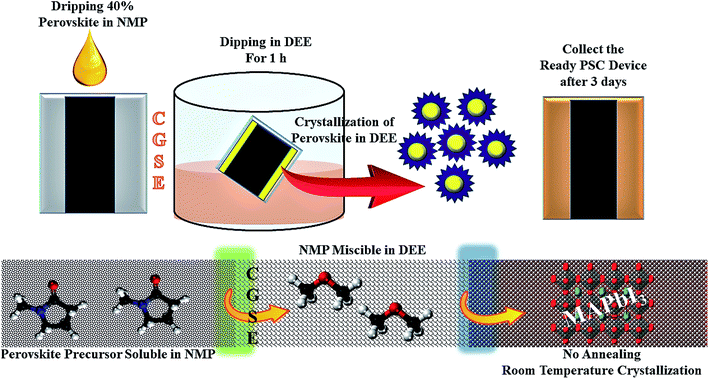 |
| | Fig. 1 Schematic illustration showing the CGSE process for the room-temperature deposition of the MAPbI3 thin film to fabricate the c-PSC. The process of perovskite formation without any heat treatment was performed for three days for fine crystallization. Exchange of N-methyl-2-pyrrolidone (NMP) with diethyl ether (DEE) helped in the formation of the pure crystal phase (the yellow arrows represent the crystal growth process by changing the solvent medium). | |
Testing approaches to determine the temperature coefficient (TC)
In order to determine the TC values, the devices fabricated were tested under two different conditions namely ST and TT. ST testing devices were placed at a particular temperature for 2 days before any further characterization. For example, at low temperature like 5 °C, it was kept in a chamber where the surrounding temperature was 5 °C and similarly at other temperatures without interference from factors like moisture and air. In contrast, for the TT testing, a single device was placed at each particular temperature using a covered vacuum temperature controller to maintain surrounding temperature (system under vacuum to avoid air and condensation) for ∼1 hour (∼30 min to reach the required temperature and then kept at that temperature for ∼30 min) for performance evaluation. A schematic of the testing details has been given in Fig. 2.
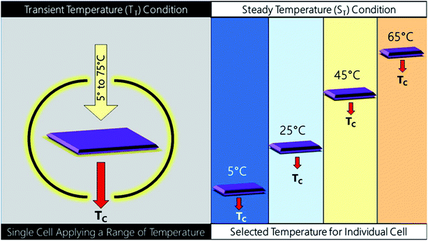 |
| | Fig. 2 Schematic of two different pathways of testing namely transient temperature testing (TT) and steady temperature testing (ST). | |
Thermal, X-ray diffraction and microstructural analyses of c-PSCs
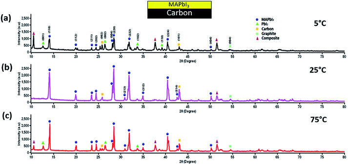
The ST devices were further investigated using scanning electron microscopy (SEM) and powder X-ray diffraction (XRD). In contrast, thermal imaging was introduced to characterize the devices under TT testing conditions. The SEM and XRD pattern of the fabricated c-PSCs under four different ST testing conditions of 5 °C, 25 °C, 45 °C and 65 °C, respectively, are shown in Fig. 3, where significant changes have been observed for different interfacial layers associated with the PSC device. ST devices were maintained at a particular temperature for two days before executing the respective characterization. For thermal images, as shown in Fig. 3, the TT testing devices were prepared as follows. At first the c-TiO2 layer was deposited over the entire fluorine-doped tin oxide (FTO) coated glass surface, and after sintering and cooling, this layer was taped from every side to reduce the surface aperture area of the next layer. In this way, successively the surface aperture area of every layer was reduced from its preceding ones to monitor the thermal imaging of the individual layer. After that, the devices were kept at a particular temperature with a covered vacuum temperature controller to maintain a similar temperature surrounding the device. Starting from the ambient conditions, for each set-temperature, 30 min was allowed to attain the set-temperature, and then it was kept for ∼30 min in order to capture the thermal images. This is how top surface thermal images of different layers separately can be obtained to record the temperature profile of the layers. Usually, the environmental temperature is variable (may be minor) throughout the day, which should affect the instantaneous thermal equilibrium of different materials due to their inherent properties. Similarly, the thermal images captured for the c-PSC can predominately correlate with outdoor circumstances where different layers could not be in instantaneous thermal equilibrium all the time. Fundamentally, different materials have different heat capacities which will have an effective influence on the disruption of the thermal equilibrium of different layers of real-world PSC devices. Thermal images at a specific temperature exhibit the nature of interfacial layers under different temperature stress. At a lower temperature, the FTO layer maintains 5 °C, whereas the compact-TiO2 layer remains at around 5.7 °C. On the other hand, m-TiO2 and m-Al2O3 layers maintain a temperature of 6.2 °C and 7 °C, respectively. The carbon layer confines the maximum amount of temperature, which is reflected in the thermal images of around 8.5 °C. It can be predicted that the temperature difference of m-TiO2, m-Al2O3 and the carbon layer can promote ion migration in this low-temperature region relative to a system in equilibrium.29 In this scenario, analysing the SEM image and XRD pattern of the devices kept at 5 °C can clarify ST behaviour. XRD data suggest the formation of PbI2 and some other intermediates at ∼5 °C. The degradation from CH3NH3PbI3 (MAPbI3) to PbI2 is most likely accompanied by a chemical reaction under thermal stress.51 On the other hand, SEM points towards spill-over of PbI2 through m-TiO2 and m-Al2O3 layers, as shown by the arrow in Fig. 3b. The spill-over is only possible due to in situ layer formation at the interfaces of the deposited layers, causing unrecognizable layer separation in the device architecture (Fig. 3b). In Fig. 3c, the XRD analysis also suggests the formation of PbI2, which triggers the spill-over, and it will affect the photovoltaic performances of devices to a great extent. At 25 °C, the separated layers of the c-PSC are quite distinct, as shown in Fig. 3d–f. Prominent layer distinction was also observed in SEM, as shown by colours in Fig. 3e and also the XRD data suggest the formation of a stable perovskite having major peaks at 14.10°, 23.47°, 28.42°, and 30.89° corresponding to the (110), (211), (220), and (310) planes of CH3NH3PbI3, respectively. Interestingly, at 25 °C, the corresponding thermal image (Fig. 3d) exhibits insignificant variation among the layers. It has also been suggested that the small amount of excess PbI2 in perovskite influences the morphology and increases the size as well as uniformity of perovskite crystals by the solvent engineering method.52
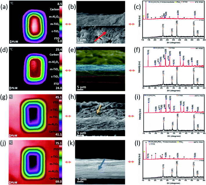 |
| | Fig. 3 (a), (b), and (c) are the top surface thermal image of the TT device, and the SEM image and XRD pattern at 5 °C for the ST device, respectively (arrow in SEM suggests the formation of an intermediate and exfoliation of PbI2); (d), (e), and (f) are the top surface thermal image of the TT device, and the SEM image and XRD pattern at 25 °C for the ST device, respectively; (g), (h), and (i) are the top surface thermal image of the TT device, and the SEM image and XRD pattern at 45 °C for the ST device, respectively (arrow in SEM suggests the initiation of intermediate formation leading to the conflation of carbon and the Al2O3 layer); (j), (k) and (l) are the top surface thermal image of the TT device, and the SEM image and XRD pattern at 65 °C for the ST device, respectively (arrow in SEM images suggests the zone of PbI2 exfoliation and conflation of layers). | |
On increasing the temperatures from 25 °C, major variations of thermal profiles on different layers were not significantly observed at 45 °C for TT devices. Analysing ST devices at 45 °C, minimal defects in both the SEM and XRD have been depicted, as shown in Fig. 3h and i, respectively. At 45 °C, the formation of low intense intermediate phases observed from the corresponding XRD study further indicates the conflation of carbon and m-Al2O3 layers as observed from the SEM image (Fig. 3h). Stepping up for much higher temperature from 45 °C to 65 °C, the pattern observed (Fig. 3j–l) was similar to that of the low temperature one for ST devices. The thermal image of the TT testing device at 65 °C indicates a relatively higher temperature of m-TiO2 and m-Al2O3 than the carbon layer, which clarifies faster ion migration within those layers as observed at the low temperature.21 The thermal images were reversible as lowering of temperature made a similar trend for TT testing. The SEM image at 65 °C signifies the factor responsible for the emergence of an interstitial layer of ST devices, Fig. 3k. This in situ layer exfoliates through other layers leading to degradation of the device performance. This may be due to the formation of an in situ intermediate structure in the interstitial position affecting the temperature transfer process, which can be confirmed by further characterization. Regarding TT devices, it is interesting to note that for all the temperature variation cases, the carbon layer possesses a relatively perceptible temperature compared to other layers of the concerned device. The effect of heating from the bottom surface, i.e. from the glass/FTO surface is therefore interpreted as an essential factor as the device is not influenced by any other external factors such as light and moisture. Fundamentally, thermal conductivity dictates the effective transfer of heat, and as the top layer, the carbon suffers from less instantaneous heating. Besides, the carbon electrode has graphite in a large amount, and previous reports show that graphite has a low thermal conductivity in a high-temperature region.53 Also, the role of specific heat capacities of materials is highly significant to maintain the temperature of the layers. From available data, it was found that the specific heat capacities of other layers are lower than that of the carbon layer (having carbon black and graphite mainly) which produces this kind of behaviour.54–56
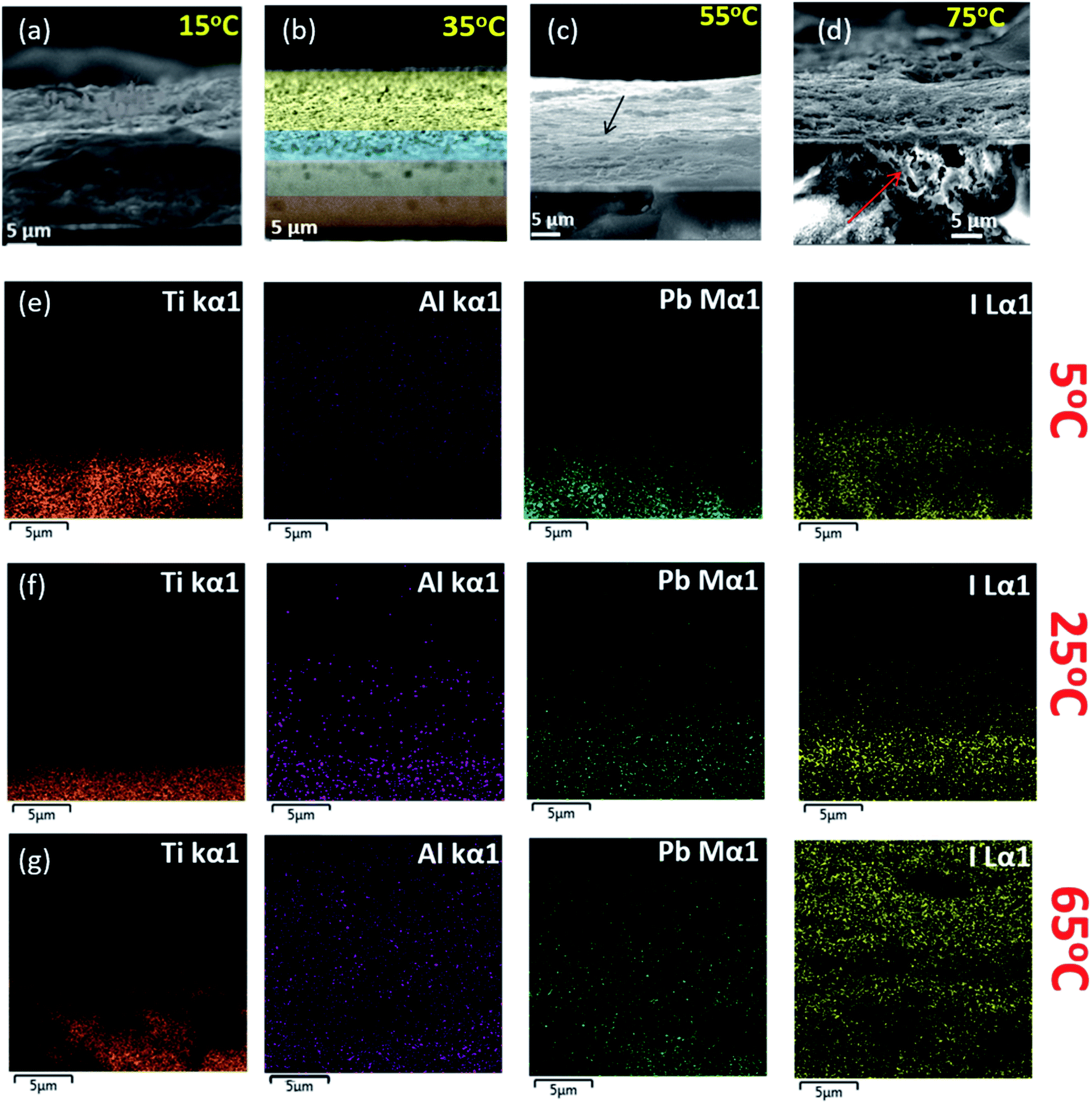
It can be one more potential reason behind this kind of thermal imaging response. Again, in a very low-temperature surrounding, the temperature dissipates very slowly from the carbon material, as shown in Fig. 3. The lower thermal conductivity of other layers along with specific heat capacity of the carbon electrode could be the reason behind this kind of significant physico-chemical response at low temperature. Materials with higher specific heat capacity have to lose a higher amount of heat energy to change their temperature during the cooling effect, which can be the primary reason for the low-temperature behaviour of the carbon electrode.57 Further study of other intermediate temperature states of ST devices has been shown in Fig. 4. The SEM images of ST devices at 15 °C, 35 °C, 55 °C and 75 °C illustrate the effect of temperature on the microstructural behaviour of the devices. The combination of layers can be seen clearly at 55 °C, and at the same time, a significant amount of degradation can be observed at very high temperature. The spill-over of the degraded material was observed in the FTO coating at 75 °C. The corresponding energy dispersive X-ray (EDX) elemental colour mapping images indicate the extent of the Pb and I formation followed by their proliferation across the different layers of the devices, as shown in Fig. 4.
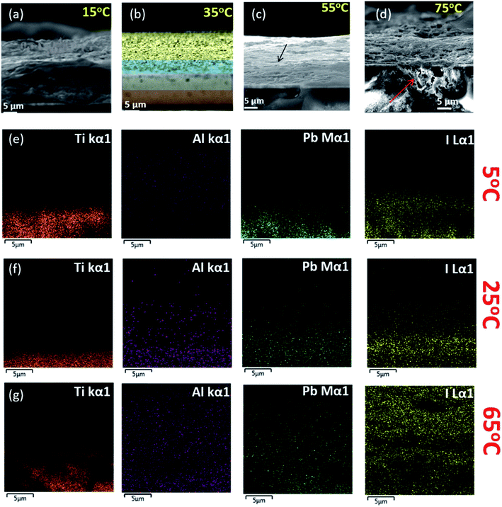 |
| | Fig. 4 (a), (b), (c), and (d) are the SEM images of ST testing devices at 15 °C, 35 °C, 55 °C, and 75 °C, respectively. (e), (f), and (g) are energy dispersive X-ray (EDX) elemental colour maps of Ti, Al, Pb, and I of the devices at 5 °C, 25 °C, and 65 °C, respectively. | |
Photovoltaic performance of c-PSCs under ST and TT conditions
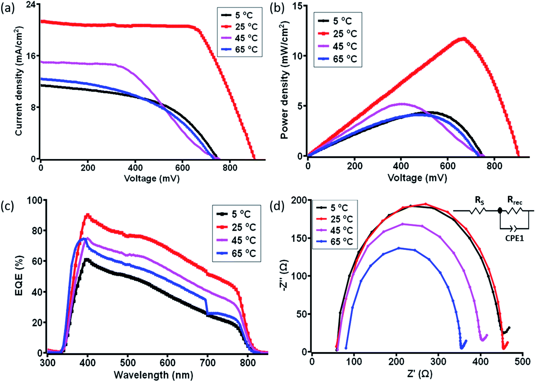
In order to understand the correlation between material characterization data and the photovoltaic parameter aspect of c-PSC devices regarding their real-world performances, the photovoltaic parameters were carefully monitored for both the ST and TT devices in the temperature window of 5 °C to 75 °C. For evaluating the performance of the as-prepared c-PSCs under ambient conditions, the current density vs. voltage (J–V) characteristic measurements were performed under 1 Sun AM 1.5 (100 mW cm−2) in the temperature range of 5 °C to 75 °C with an increment of 10 °C considered as ST condition. The recorded J–V characteristic parameters are further compared in Table 1. Interestingly, starting from 5 to 25 °C there was a steady increase in the device PCE, followed by a maximum PCE achieved as 13.1% at 25 °C. After that, a decline of PCE was noticed up to 40 °C, and from 45 to 75 °C, the PCE dropped down extensively. Poor performance at higher temperatures is expected due to the degradation of MAPbI3, but the initiation of degradation and its impression on the different layers are still uncovered and need to be addressed.28,29Fig. 5a and b describes the major J–V characteristics and power density plots at four significant temperatures of the ST devices, respectively, whereas the overall J–V characteristic plot recorded for ST variations has been shown in Fig. S1a and b, ESI.† The variation of photovoltaic performances was measured for a set of five devices at each temperature, as shown in Fig. S2, ESI.†
Table 1 Photovoltaic parameters of ST c-PSC under 1 Sun 1.5G AM (active area of 0.12 cm2)
| Temperature (°C) |
J
SC (mA cm−2) |
V
OC (mV) |
FF |
PCEmax (%) |
Powermax (mW cm−2) |
| 5 |
11.42 |
752.6 |
0.51 |
4.34 |
4.32 |
| 15 |
16.64 |
758.8 |
0.65 |
8.34 |
7.84 |
| 25 |
21.34 |
905.1 |
0.68 |
12.0 |
13.11 |
| 35 |
20.12 |
902.1 |
0.54 |
9.7 |
9.62 |
| 45 |
15.30 |
759.2 |
0.48 |
5.50 |
5.15 |
| 55 |
15.16 |
748.6 |
0.45 |
5.14 |
4.93 |
| 65 |
12.43 |
734.7 |
0.45 |
4.10 |
4.15 |
| 75 |
12.32 |
740.3 |
0.42 |
3.87 |
3.76 |
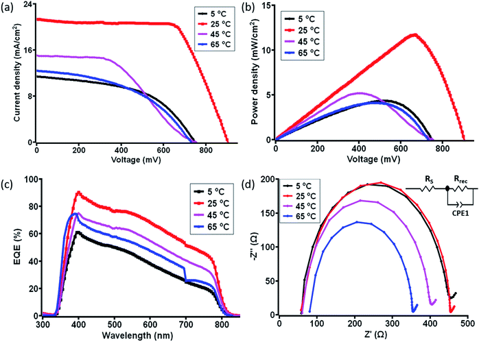 |
| | Fig. 5 (a) Current density–voltage (J–V) curves and (b) power density–voltage curve for the ST c-PSCs at different temperatures in the range of 5 °C to 75 °C, (c) IPCE spectra of c-PSCs at different temperatures, and (d) corresponding EIS characteristics (Nyquist plots) with the fitted circuit diagram for ST devices having the best performance. | |
In addition, the external quantum efficiency (EQE) curves of c-PSCs exhibited a broad peak over the range of 300–800 nm with a maximum value of ∼90% for the devices at 25 °C at a wavelength of 450 nm showing high charge collection efficiency in devices as shown in Fig. 5c and S1c, ESI.† It has been observed that the EQE values are relatively lower at a lower or higher temperature compared to 25 °C. Higher values of EQE signify higher charge carrier collection for the solar cell and a slow charge recombination process.58 Further, the integrated JSC for samples at different temperatures was evaluated from the overlap integral of the IPCE spectra, and values are given in Table S1, ESI.† The average integrated JSC values of c-PSCs at different temperatures are almost similar to the JSC values obtained from the J–V analysis.
Further, electrochemical impedance spectroscopy (EIS) studies encourage us to understand the transport properties at different interfaces of layers in the ST c-PSC device. The Nyquist plot with an equivalent circuit diagram of the considered c-PSCs was recorded in the dark at 0.8 V bias from 10 mHz to 1 MHz, as shown in Fig. 5d and S1d, ESI.† In the circuit diagram (inset of Fig. 5d), RS represents the series resistance, which includes the resistance of FTO and the carbon counter electrode. Rrec is the charge transfer resistance at the perovskite/carbon interface.59 In Fig. 5d, the large parabola in the high-frequency region implies higher transportation and exchange resistance from the perovskite to the carbon counter electrode, which will influence the fill factor as reflected from J–V characterization. Again, higher values of RS should diminish the efficiency, and depending on temperature variation RS values can be observed from Table S1, ESI.†
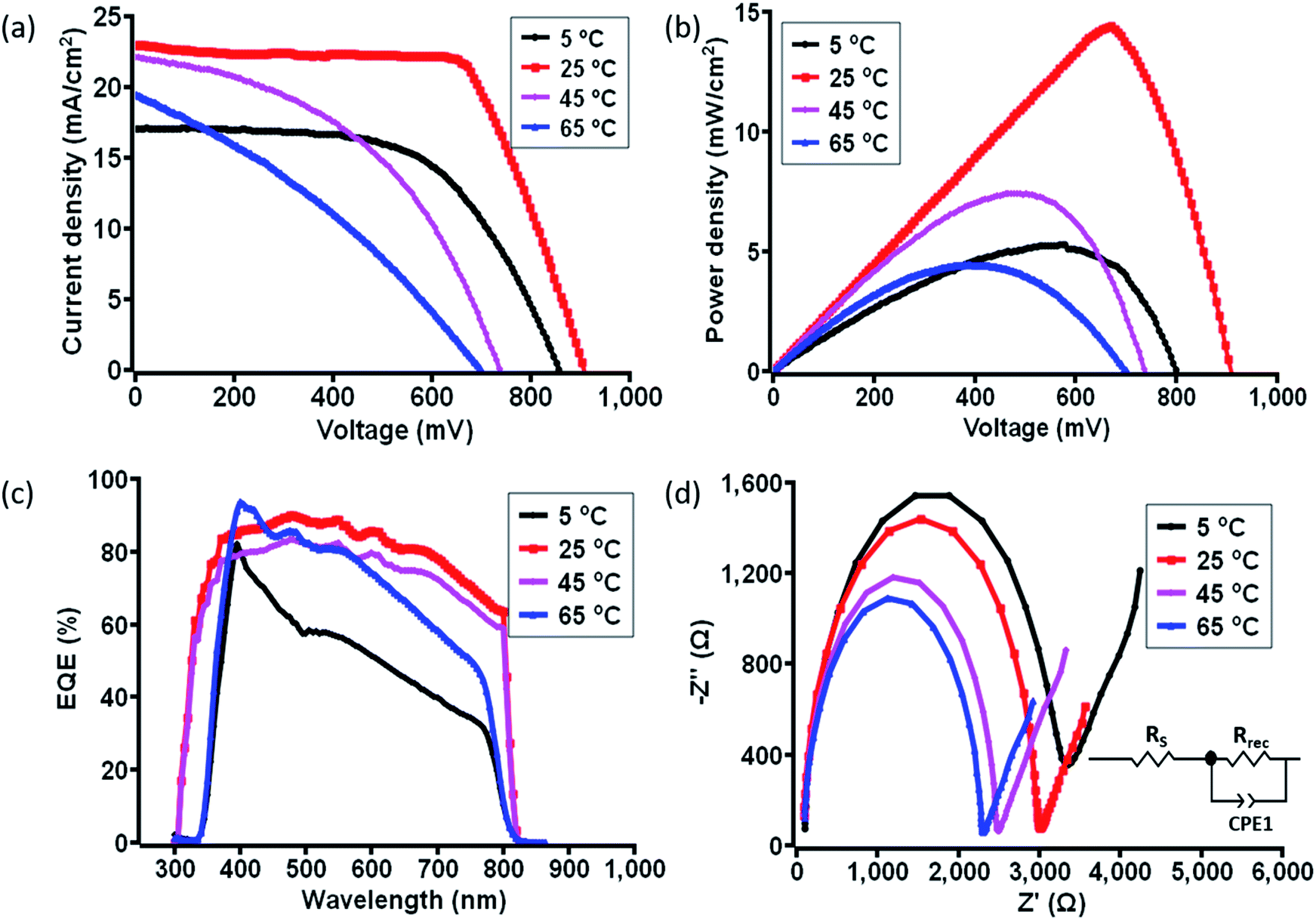
Despite the ST observation, a c-PSC device can withstand a wide range of temperatures. In order to understand the instantaneous behaviour of the photovoltaic performance, a c-PSC device was further employed for TT testing. In this case, the performance of the c-PSC devices was also examined in the same way in the temperature range of 5 to 75 °C with an increment of 5 °C. Similarly, the temperature was allowed to decrease from 75 to 5 °C and the data were recorded at an interval of every 5 °C. The overall tuning of the temperature window was repeated twice on the same c-PSC device. The obtained reversible nature of parameters of the champion device is given in the ESI (Fig. S5†). It has been observed that the PCE was reduced by ∼10% during the transition from high to low temperature. However, the PCE regained almost its initial value when the device was heated back from low temperature. This particular behaviour signifies a negligible effect on the TC. The maximum PCE of 14.4% was observed at 25 °C (Fig. 6a), and then a consistent decrease in PCE was reflected during stepping up or stepping down to higher and lower temperatures, respectively. Fig. 6a and b describe the major J–V characteristics and power density plots at four significant temperatures of the TT devices, respectively. The performance of all other temperatures is given in Fig. S3a and b, ESI.† The continuous temperature change may have triggered some internal modifications in the devices, which can be responsible for this phenomenon. The variation of performances was measured for a set of five devices at each temperature, as shown in Fig. S4, ESI.† EQE data of TT c-PSCs exhibited a broad peak over the range of 300–800 nm with a maximum value of ∼90% for the device at 25 °C at a wavelength of 450 nm indicating a higher rate of charge collection efficiency in devices as shown in Fig. 6c and S3c, ESI.† From the overlap integral of the IPCE spectra, integrated JSC values were evaluated, and values are mentioned in Table S2, ESI.† Besides, the corresponding EIS measurements of TT devices are shown in Fig. 6d and S3d, ESI,† which reflect a similar nature of data obtained from J–V characterization. The RS and Rrec values, as recorded from EIS analysis, are mentioned in Table S2, ESI.† The photovoltaic performances under both ST and TT conditions show the influence of interface passivation on the operating temperature of PSCs. The energy barrier, the defects or charge or ion accumulation at perovskite-transport material interfaces, ions in perovskite or charge transport layers, and charge mobility in charge transport layers determine not only the charge collection efficiency but also have a significant impact on the hysteresis.60 Though the interfacial layers avoid the direct contact of the perovskite film with metal electrodes, the inherent mobile iodide ions in the perovskite film can easily diffuse across the interfacial materials to react with the electrode due to the minimal activation energy for their migration.
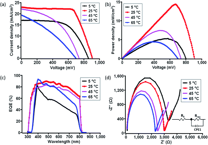 |
| | Fig. 6 (a) Current density–voltage curves and (b) power density–voltage curve for the best TT c-PSC at different temperatures in the range of 5 to 75 °C. Photovoltaic characterization of the best TT device for each temperature in the range of 5 °C to 75 °C, (c) IPCE spectra of c-PSCs at different temperatures, and (d) corresponding EIS characteristics (Nyquist plots) with the fitted circuit diagram for the TT device having the best performance. | |
Evaluation of TC from the ST and TT testing devices
The temperature coefficients quite delineate the behaviour of the c-PSC's photovoltaic parameter function of the temperature. Determination of the temperature coefficient (TC) of these two types of testing for c-PSC devices applying the generalized linear relation becomes very much essential for a better understanding of the temperature–performance correlation in real-world condition as mentioned in the following equations (eqn (i)–(iv))34,41where JTC is the temperature coefficient of current density, ΔJ is the difference of short-circuit current density at a particular temperature with respect to the reference temperature (reference temperature is 25 °C), Jref is current density at the reference temperature, VTC is the temperature coefficient of open-circuit voltage, ΔV is the difference of open-circuit voltage at a particular temperature with respect to the reference temperature, Vref is the open-circuit voltage at the reference temperature, ηTC is the efficiency temperature coefficient (ETC)/°C, Δη is the difference of efficiency at a particular temperature with respect to the reference temperature, ηref is the efficiency at the reference temperature, PTC is the temperature coefficient of power density, ΔP is the difference of power density at a particular temperature with respect to the reference temperature, Pref is the power density at the reference temperature, and ΔT is the temperature difference between device temperature and reference temperature. Using eqn (i)–(iv) quite a remarkable trend was obtained in the TC values for ST and TT processes.
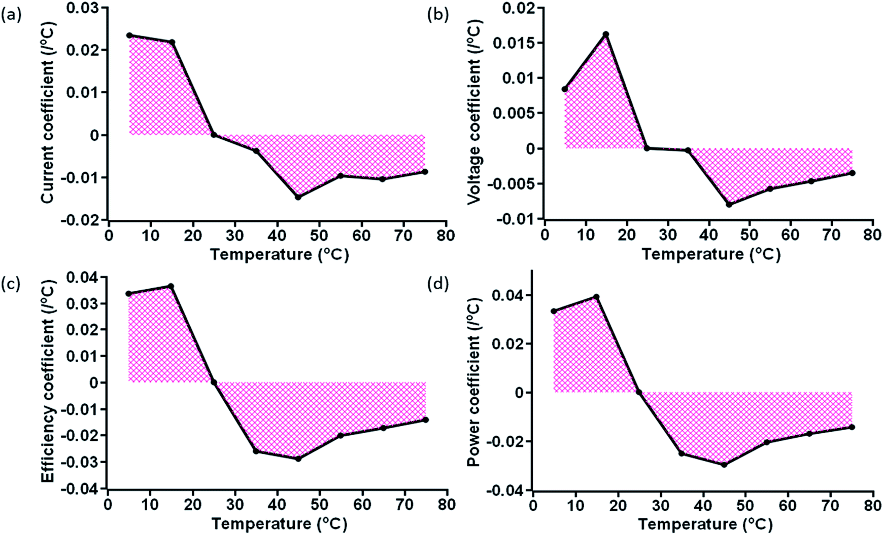
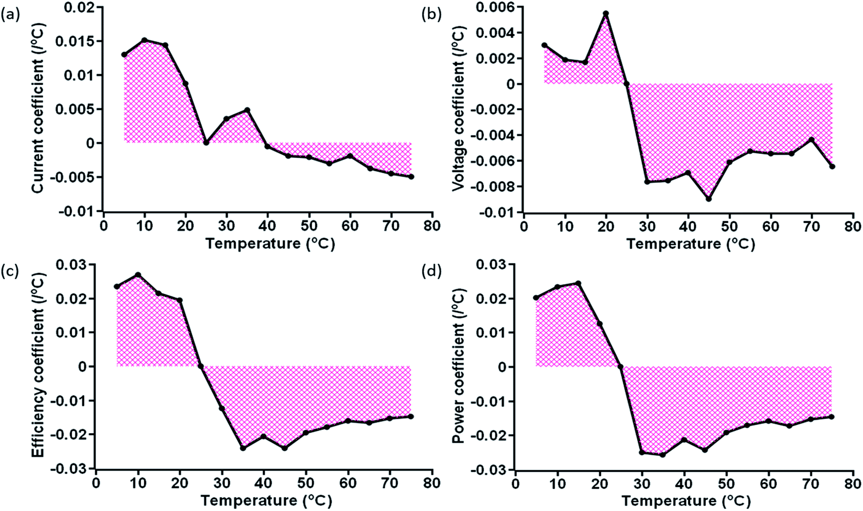
The variation of obtained TC values at specific temperature is shown in Fig. 7 and 8, for ST and TT methods, respectively. A clear distinction of the average TC values is acquired for ST and TT processes, as shown in Table 3. The average TC values of current density for ST and TT conditions have significant discrimination from each other. In the case of the TT process, the current density increases from 5 to 35 °C, but for ST testing, the increase occurs up to 25 °C. TC values of other parameters for two different scenarios seem to be close. However, these variations lead to significant differences in the PCE and other parameters of devices under two different testing conditions, as shown in Tables 1 and 2. Also, the conditions are entirely different in these two testing states, which makes TC values more significant. Moreover, the TC values resulting from TT testing conditions are reversible, whereas ST testing devices do not show such behaviour, hence resulting in faster degradation.
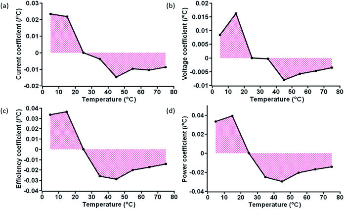 |
| | Fig. 7 Area plot of the variation of the (a) current coefficient, (b) voltage coefficient, (c) efficiency coefficient, and (d) power coefficient at specific temperatures for ST devices. | |
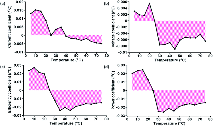 |
| | Fig. 8 Area plot of the variation of the (a) current coefficient, (b) voltage coefficient, (c) efficiency coefficient, and (d) power coefficient at specific temperatures for TT devices. | |
Table 2 Photovoltaic parameters of the TT c-PSC under 1 Sun 1.5G AM (active area of 0.12 cm2)
| Temperature (°C) |
J
SC (mA cm−2) |
V
OC (mV) |
FF |
PCEmax (%) |
Powermax (mW cm−2) |
| 5 |
17.0 |
860.0 |
0.59 |
8.62 |
8.65 |
| 10 |
17.74 |
891.4 |
0.60 |
9.44 |
9.38 |
| 15 |
19.69 |
895.3 |
0.65 |
11.30 |
11.1 |
| 20 |
22.0 |
894.5 |
0.68 |
13.57 |
12.94 |
| 25 |
23.0 |
915.0 |
0.69 |
14.50 |
14.43 |
| 30 |
23.36 |
872.1 |
0.66 |
13.40 |
13.14 |
| 35 |
24.06 |
835.8 |
0.55 |
11.06 |
11.02 |
| 40 |
22.82 |
805.9 |
0.54 |
9.80 |
9.54 |
| 45 |
22.13 |
742.0 |
0.45 |
7.47 |
7.35 |
| 50 |
21.79 |
768.4 |
0.44 |
7.36 |
7.37 |
| 55 |
20.92 |
746.1 |
0.42 |
6.54 |
6.48 |
| 60 |
21.45 |
758.3 |
0.40 |
6.44 |
6.25 |
| 65 |
19.49 |
703.5 |
0.33 |
4.48 |
4.38 |
| 70 |
18.37 |
736.2 |
0.33 |
4.51 |
4.48 |
| 75 |
17.34 |
679.9 |
0.33 |
3.80 |
3.57 |
Table 3 Average values of temperature coefficients for ST and TT testing devices in different temperature ranges (NA: not applicable)
| Temperature (T) range (°C) |
Average temperature coefficient of JSC (×10−2) |
Average temperature coefficient of VOC (×10−2) |
Average temperature coefficient of PCEmax (×10−2) |
Average temperature coefficient of power densitymax (×10−2) |
|
S
T
testing
|
| 5 ≤ T ≤ 25 |
+2.3 |
+1.2 |
+3.5 |
+3.6 |
| 25 ≤ T ≤ 75 |
−0.9 |
−0.4 |
−2.1 |
−2.2 |
![[thin space (1/6-em)]](https://www.rsc.org/images/entities/char_2009.gif) |
|
T
T
testing
|
| 5 ≤ T ≤ 25 |
+1.2 |
+0.3 |
+2.5 |
+2.0 |
| 25 ≤ T ≤ 35 |
+0.4 |
NA |
NA |
NA |
| 35 ≤ T ≤ 75 |
−0.3 |
NA |
NA |
NA |
| 25 ≤ T ≤ 75 |
NA |
−0.6 |
−1.8 |
−1.9 |
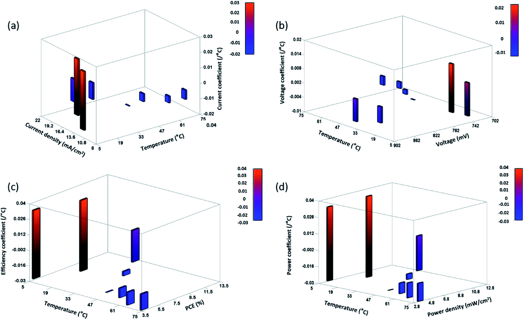
Besides, the temperature-dependent TC exhibits interesting features under various photovoltaic parameters, and temperatures as shown by three-dimensional (3D) representation plots in Fig. 9 and 10. The figures dictate a similarity in TC as reported for other traditional solar cells only in the high-temperature region (negative TC) but not at temperatures below STC (positive TC for the c-PSC), which can make them a more front runner for commercialization.22 The difference in TC plots of ST and TT testing is fascinating as well for real-world performance analysis.
 |
| | Fig. 9 3D bar plot of the (a) current coefficient, (b) voltage coefficient, (c) efficiency coefficient, and (d) power coefficient at the specific temperature and corresponding parameters for ST devices. | |
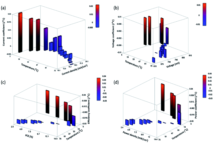 |
| | Fig. 10 3D bar plot of the (a) current coefficient, (b) voltage coefficient, (c) efficiency coefficient, and (d) power coefficient with respect to temperature, and corresponding parameters for TT devices. | |
During the TT testing (Fig. 8), the stabilized TC values show that the TT c-PCSs are more suitable in those parts of the world where temperature variation throughout the day is very high. On the other hand, ST temperature conditions can notably be considered in those parts where the variation of weather in a day is very low throughout a particular season. Moreover, the lower TC value for a c-PSC makes it a suitable candidate for a multi-junction solar cell.
An overall analysis of c-PSCs under ST testing conditions
It is now highly relevant to realize the variation of TC values or rather the performances with in-depth analysis, for which further investigation was performed to recognize the probable origin concerning the associated layers of the device. The MAPbI3 actually controls the device performance, and further its stability.61 Thus, it is crucial to investigate the role of MAPbI3 across the different layers of the c-PSC under thermal stress. In order to understand such effects, three different sets of films were prepared on an FTO glass namely (a) spin-coated m-TiO2 and MAPbI3, (b) spin coated m-Al2O3 and MAPbI3, and (c) screen printed carbon and spin coated MAPbI3 under ST conditions.
The XRD patterns at 5 °C and 65 °C for Al2O3 based films exhibit quite distinct characteristics, as shown in Fig. S6, ESI.† It has been observed that at the low temperature the appearance of unwanted PbI2 is less pronounced compared to the higher temperature. Besides, PbI2 tends to cover the Al2O3 layer to some extent, which eases the exfoliation of PbI2 formed in the interstitial position. On the other hand, for the m-TiO2 coated samples, it was found that the extent of PbI2 formation at both high and low temperatures is quite truncated, as shown in Fig. S7, ESI.† Due to the lower formation of PbI2 weak exfoliation through the TiO2 layer is expected. Again, for the carbon-based layer, a substantial amount of information was obtained to understand the low efficiencies at temperatures 5 °C and 75 °C for the ST devices. The XRD pattern suggests the formation of an intermediate state by the interaction of carbon and perovskite or a degraded perovskite due to thermal treatment, as shown in Fig. 11. This further leads to more extensive degradation of MAPbI3.
 |
| | Fig. 11 (a), (b), and (c) XRD data of glass samples coated with WO3 doped carbon and perovskite at 5 °C, 25 °C, and 75 °C, respectively showing the formation of an intermediate state. | |
The appearance of the PbI2 phase facilitates increased exfoliation through the layer of the c-PSC. The combination of a newly formed unrecognizable intermediate and formation of PbI2 severely damages the performances of devices at very high and low-temperature regions. The SEM images also defended the formation of an intermediate phase with carbon, as shown in Fig. S8, ESI.† At 25 °C, the SEM image (Fig. S8c, ESI†) shows a prominent surface structure, but dissimilarity can also be observed with temperature variation. On the other hand, the SEM analysis indicates that a rapid change occurred at 15 °C and 45 °C for the ST devices. The results suggest the initialization of intermediate formation, which points towards a rapid decrease in efficiency at those temperatures. On, the other hand, extrinsic accumulation of I− plays a great role in exfoliation through Al2O3 and TiO2 layers. The extent of degradation is greater when MAPbI3 interacts with Al2O3 rather than TiO2. This elucidates the predominant spill-over of perovskite through the Al2O3 layer in the ST testing devices. The interaction of the carbon layer and perovskite greatly influences the device performance via the formation of intermediates, and as a whole, the interface of carbon and Al2O3 is expected to initiate perovskite deformation. At temperatures above 45 °C and below 15 °C for ST testing, “pinhole structures” are created, which clearly verifies inter-molecular interaction leading to intermediate formation for devices as shown in SEM (Fig. S8, ESI†).32 The XRD pattern, as shown in Fig. 11, further confirms the formation of such intermediate structures between carbon and MAPbI3 upon exposure to different temperatures for more than a day. The heat produced by high temperature also initiates the chemical decomposition of the MAPbI3 film. In this case, the interfacial layers have the direct contact of the MAPbI3 film with the electrode, and the inherent mobile halide ions in the perovskite film can easily diffuse across the interfacial materials to react with the electrode due to the minimal activation energy for their migration. The heat generated at high temperature was also reported to cause migration of metal atoms into PSCs, leading to the degradation of the devices.61 At the same time, corrosion occurring from the active carbon and Al2O3 layer by either the iodide in the perovskite film or the decomposed by-product such as volatile I2 and HI has also become a significant concern for high-temperature stress for the operation of the PSC. Temperature stress can produce thermal exfoliation of the layers as observed from different temperature-based SEM analyses, as obtained from Fig. 3. Exfoliation decreases the reachable aperture area of the layers concerned, which accordingly retards the performance of devices. However, the degradation of the device performance of PSCs has also been observed at a lower temperature for ST testing. It is observed that at low temperatures the orientation of the methylammonium cation in MAPbI3 is fixed because of hydrogen bonding between the NH3 groups and the framework iodide atoms. This acts as the driving force for the observed deformation of the PbI3− framework and further adopting a staggered formation. As the temperature is increased the thermal motion of the cation increases and the NH–I interactions weaken.61 It seems that, in general, the growth of metal oxide might give rise to the lowering of interface quality. This might be related to the presence of surface defects in metal oxides, which lead to high interface recombination.62 Also, there will be a slight influence of surrounding moisture and air, although the devices were kept inside a chamber of fixed temperature. It was suggested that excess PbI2 in MAPbI3 could help to passivate defects at surfaces and grain boundaries and a small amount of residual PbI2 in perovskite helps to reduce charge recombination and improves the VOC and FF.59 As a result, the devices do not lose their VOC under thermal stress, indicating the PCE loss is mainly restricted to the JSC. This kind of materialistic interface dependent performance variation with respect to temperature is highly demanded for real-world application of c-PSCs. The discussions mentioned above have been further schematically described in Fig. 12.
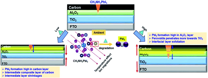 |
| | Fig. 12 Schematic view of high, low, and ambient temperature effect on a c-PSC. | |
An overall analysis of c-PSCs under TT testing conditions
T
T testing signifies the unique effects of temperature variations on a particular device. The presence of a temperature gradient between the layers significantly influenced the performance. The perovskite can become chemically unstable at temperatures well below its decomposition conditions due to the temperature gradient.21 Migration of mobile ions by the influence of temperature stress (majorly iodide ion) is responsible for PSCs' unique and prominent properties, although the large-scale trapping of electrons cannot be ruled out.63–65 Most of the studies suggest that, with temperature, the mobility of transient ions increases, which leads to the accumulation of ions at interfacial contacts of the perovskite and other layers. As the work function of the HTL and ETL differs from each other, this difference creates a built-in field, which drives the migratory ions. Temperature variation can reduce the built-in field, which eventually can increase the extent of ion migration. Thus, the excess mobility of ions leads to accumulation of ions at interfaces. Accumulation of ions reduces current generation due to the increase in the recombination process at interfaces by increasing bandgap defects or electrostatic traps.66–69 Data obtained from EIS (Fig. 6) confirm high charge recombination resistance pointing towards the hike in the recombination process for the TT study. The role of crystal lattice disruption of perovskite (tetragonal to cubic) at a temperature higher than 50 °C cannot be neglected, which significantly reduces the performance of TT devices.70 On the other hand, the thermal expansion coefficients of different materials used can significantly disrupt the interconnectivity of layers, increasing the interfacial defects.70 The variation of performance at low temperature may be the result of this expansion factor. Also, the effect of low charge diffusion cannot be neglected at low temperature, which can reduce performance.71 A correlation between ST and TT observations can be drawn from this experiment. It is explained earlier that intrinsic ion migration and accumulation may be the reason behind the performance loss of TT devices. Because of thermal stress on the TT devices, defect states may occur followed by creation of interstitial vacancies.64 Iodide ions could drift across the interface, and enter the vacant positions. The intermediate formation in ST devices could have originated from the intrinsic behaviour of TT devices. However, the exact nature of the intermediate phase needs clarity leading to research that is more intensive. To the best of our knowledge, we are the first to report the TC aspect of carbon-based PSCs. It is anticipated that temperature can significantly influence the photovoltaic parameters of the device. The way of temperature treatment is further indicative of the c-PSCs' photovoltaic behaviour, which has been depicted in terms of TC for the real-world condition. In this study, we propose that the average TC values should closely agree with the observed trend of this study for any c-PSC or rather any PSC. The challenge is the development of advanced high-temperature resistant PSCs, and modules based on novel architectures and/or processes, which can tackle efficiency limitations while improving cost-effectiveness.
Conclusions
In conclusion, we have investigated the temperature coefficient (TC) of carbon-based perovskite solar cells (c-PSCs) in two determining ways namely under steady temperature (ST) and transient temperature (TT) conditions across a broad temperature window from 5 to 75 °C. These explorations provide new insights into a PSC by means of TC analysis based on corresponding different photovoltaic parameters. Highly noticeable performance in short circuit current, open-circuit voltage, fill factor, and power conversion efficiency of the devices as a function of temperature was observed, leading to distinct TC values separately for the ST and TT cases. Instantaneous behaviour is pronounced in the case of TT devices leading to rapid changes due to ion migration and accumulation at interfaces across the c-PSC device. We have observed that the TC value becomes higher for ST testing devices compared to TT, which is further explained by various interfacial layer physicochemical studies. The TC values derived from TT testing conditions are reversible, whereas the irreversible TC value of ST testing shows degradation of the devices. Effect of temperature on the different interfacial layers of the c-PSC and their correlation with the photovoltaic performances have been further established. The XRD and SEM microstructural analyses further suggested that the extent of perovskite degradation was greater at the Al2O3–perovskite interface due to the thermal stress. The observed dual characteristics of TC for a c-PSC in a low and high-temperature region attract future research interest for its large-scale real-world condition testing. Future studies will be further required to investigate whether other architectures of PSCs or other organo-metal halide perovskites are more robust to the TC parameter variation. The temperature-dependent surface features of the perovskite also highlight the role of the interfacial interaction associated with the different layers in the photovoltaic performance of the solar cells. We assume that further research about the origin of thermal stress on various interfacial layers might help in reducing the photocurrent loss, thereby increasing the likelihood of successful outdoor application of PSCs.
Materials and methods
CH3NH3PbI3 synthesis and c-PSC device fabrication
Fabrication of c-PSCs was adopted from our earlier reported article with slight modification using the ‘crystal growth via solvent exchange’ (CGSE) method for better performance.65 In short, sequential deposition of compact TiO2 (c-TiO2), mesoporous TiO2 (m-TiO2), mesoporous Al2O3, and WO3 incorporated carbon was performed on a fluorine-doped tin oxide (FTO) glass substrate. The perovskite precursor (MAPbI3) solution was drop-cast, followed by spin coating, and then the CGSE method was deduced from previous literature.50 CGSE stands out as an effective one-step approach for the fabrication of organic hole-conductor free carbon-based perovskite solar cells with superior device performance. At the same time, the room-temperature solution processing fabrication method allows us to develop crystalline, scalable, and rapid perovskite thin films with no further heat-treatment. In the CGSE process, coated FTO glasses were immersed in a diethyl ether (DEE) bath for 1 hour at room temperature instead of thermal annealing. During the CGSE process, the NMP soluble MAPbI3 precursor is exposed to DEE, and the NMP solvent is extracted selectively because NMP is highly miscible in DEE. This triggers the crystallization of MAPbI3 perovskite in areas devoid of NMP, which spreads rapidly to cover the entire area as NMP is completely extracted by DEE. A schematic diagram has been mentioned, which illustrated the CGSE process as shown in Fig. 1. The as prepared devices were kept under dry and dark conditions for three days to obtain a uniform growth of perovskite crystals. Finally, the c-PSCs were subjected to further characterization and measurements. The prepared c-PSC devices were divided into two groups before further characterization under ST and TT conditions (Fig. 2). ST resembles separate devices kept at different temperatures and TT indicates that a particular device has been tested under variable temperature conditions. ST devices were again classified into sub-groups depending on temperature rather in the case of TT devices, where there were no sub-groups.
Material characterization
The infra-red (IR) camera shots (thermal images) were taken with a FLIR T425 camera positioned on top of the PSC kept at every different temperature at the base by 10 mm. The cross-sectional thickness measurement and elemental mapping of the PSC were performed on a scanning electron microscope (SEM-EDX), (LEO 430i, Carl Zeiss). X-ray diffraction (XRD) analysis of the fabricated PSC films was carried out on an X'pert pro MPD XRD of PAN analytical with Cu Kα radiation (λ = 1.5406 Å). Further, testing of the PSC was executed under 1000 W m−2 of light from a Wacom AAA continuous solar simulator (model: WXS-210S-20, AM1.5G). The I–V characteristic of the devices was recorded using an EKO MP-160i I–V Tracer. EIS measurements were carried out with an AUTOLAB frequency analyzer setup equipped with an AUTOLAB PGSTAT 10 and a Frequency Response Analyzer (FRA) Module. The measurements were performed under the same solar simulator condition with the frequency range from 10 mHz to 1 MHz. All the devices were measured at the 0.80 V open-circuit voltage of the devices. The experimental data were fitted with the Z-view software (version 3.4d, Scribner Associates, Inc., USA) using appropriate equivalent circuits. Incident photon to current efficiency (IPCE) was measured on a BENTHAM PVE300 Photovoltaic EQE (IPCE), and IQE solution under 350–750 nm wavelength using a tungsten halogen lamp source.72 All the data presented are an average of measurements taken on five different devices.
Data availability statements
The data that support the plots within this paper, and other findings of this study are available from the corresponding author upon reasonable request.
Conflicts of interest
The authors declare no conflicts of interest.
Acknowledgements
S. B. acknowledges the College of Engineering, Mathematics, and Physical Sciences, the University of Exeter for his PhD fellowship. Partial funding from the EPSRC funded JUICE project (EP/P003605/1) is acknowledged.
Notes and references
- J. Yan and B. R. Saunders, RSC Adv., 2014, 4, 43286–43314 RSC.
- N. Torabi, A. Behjat, Y. Zhou, P. Docampo, R. J. Stoddard, H. W. Hillhouse and T. Ameri, Materials Today Energy, 2019, 12, 70–94 CrossRef.
- A. Kojima, K. Teshima, Y. Shirai and T. Miyasaka, J. Am. Chem. Soc., 2009, 131, 6050–6051 CrossRef CAS.
- H.-S. Kim, C.-R. Lee, J.-H. Im, K.-B. Lee, T. Moehl, A. Marchioro, S.-J. Moon, R. Humphry-Baker, J.-H. Yum, J. E. Moser, M. Grätzel and N.-G. Park, Sci. Rep., 2012, 2, 591 CrossRef.
- G. Grancini, C. Roldán-Carmona, I. Zimmermann, E. Mosconi, X. Lee, D. Martineau, S. Narbey, F. Oswald, F. De Angelis, M. Graetzel and M. K. Nazeeruddin, Nat. Commun., 2017, 8, 15684 CrossRef CAS.
- F. Meng, A. Liu, L. Gao, J. Cao, Y. Yan, N. Wang, M. Fan, G. Wei and T. Ma, J. Mater. Chem. A, 2019, 7, 8690–8699 RSC.
-
Best Research-Cell Efficiency Chart, https://www.nrel.gov/pv/cell-efficiency.html, 2019 Search PubMed.
- I. Y. Choi, C. U. Kim, W. Park, H. Lee, M. H. Song, K. K. Hong, S. Il Seok and K. J. Choi, Nano Energy, 2019, 65, 104044 CrossRef CAS.
- T. D. Siegler, T. M. Shimpi, W. S. Sampath and B. A. Korgel, Chem. Eng. Sci., 2019, 199, 388–397 CrossRef CAS.
-
D. Forgacs, K. Wojciechowski and O. Malinkiewicz, Perovskite Photovoltaics: From Laboratory to Industry, ed. V. Petrova-Koch, R. Hezel and A. Goetzberger, Springer International Publishing, Cham, 2020, pp. 219–255 Search PubMed.
- A. Ghosh, S. Bhandari, S. Sundaram and T. K. Mallick, Renewable Energy, 2020, 145, 2151–2158 CrossRef CAS.
- M. M. Lee, J. Teuscher, T. Miyasaka, T. N. Murakami and H. J. Snaith, Science, 2012, 338, 643–647 CrossRef CAS.
- A. Abate, J.-P. Correa-Baena, M. Saliba, M. S. Su'ait and F. Bella, Chem.–Eur. J., 2018, 24, 3083–3100 CrossRef CAS.
- A. Bashir, S. Shukla, J. H. Lew, S. Shukla, A. Bruno, D. Gupta, T. Baikie, R. Patidar, Z. Akhter, A. Priyadarshi, N. Mathews and S. G. Mhaisalkar, Nanoscale, 2018, 10, 2341–2350 RSC.
- M. Batmunkh, C. J. Shearer, M. J. Biggs and J. G. Shapter, J. Mater. Chem. A, 2015, 3, 9020–9031 RSC.
- H. Chen and S. Yang, Adv. Mater., 2017, 29, 1603994 CrossRef.
- S. Collavini and J. L. Delgado, Adv. Energy Mater., 2017, 7, 1601000 CrossRef.
- M. Duan, Y. Hu, A. Mei, Y. Rong and H. Han, Materials Today Energy, 2018, 7, 221–231 CrossRef.
- F. Meng, L. Gao, Y. Yan, J. Cao, N. Wang, T. Wang and T. Ma, Carbon, 2019, 145, 290–296 CrossRef CAS.
- R. Wang, M. Mujahid, Y. Duan, Z.-K. Wang, J. Xue and Y. Yang, Adv. Funct. Mater., 2019, 29, 1808843 CrossRef CAS.
- X. Wang, H. Liu, F. Zhou, J. Dahan, X. Wang, Z. Li and W. Shen, ACS Appl. Mater. Interfaces, 2018, 10, 835–844 CrossRef CAS.
- A. Roy, A. Ghosh, S. Bhandari, S. Sundaram and T. K. Mallick, Ind. Eng. Chem. Res., 2020, 59, 11063–11071 CrossRef CAS.
- S. Bhandari, A. Roy, T. K. Mallick and S. Sundaram, Mater. Lett., 2020, 268, 127568 CrossRef CAS.
- M. Hadadian, J.-H. Smått and J.-P. Correa-Baena, Energy Environ. Sci., 2020, 13, 1377–1407 RSC.
- Q. Wang, W. Zhang, Z. Zhang, S. Liu, J. Wu, Y. Guan, A. Mei, Y. Rong, Y. Hu and H. Han, Adv. Energy Mater., 2020, 10, 1903092 CrossRef CAS.
- L. K. Ono, S. R. Raga, S. Wang, Y. Kato and Y. Qi, J. Mater. Chem. A, 2015, 3, 9074–9080 RSC.
- G. Mannino, A. Alberti, I. Deretzis, E. Smecca, S. Sanzaro, Y. Numata, T. Miyasaka and A. La Magna, J. Phys. Chem. C, 2017, 121, 7703–7710 CrossRef.
- R. B. Dunbar, W. Moustafa, A. R. Pascoe, T. W. Jones, K. F. Anderson, Y.-B. Cheng, C. J. Fell and G. J. Wilson, Prog. Photovoltaics Res. Appl., 2017, 25, 533–544 CrossRef CAS.
- R. Cao, F. Xu, J. Zhu, S. Ge, W. Wang, H. Xu, R. Xu, Y. Wu, Z. Ma, F. Hong and Z. Jiang, Adv. Energy Mater., 2016, 6, 1600814 CrossRef.
- H. Zhang, X. Qiao, Y. Shen, T. Moehl, S. M. Zakeeruddin, M. Grätzel and M. Wang, J. Mater. Chem. A, 2015, 3, 11762–11767 RSC.
- J. A. Schwenzer, L. Rakocevic, R. Gehlhaar, T. Abzieher, S. Gharibzadeh, S. Moghadamzadeh, A. Quintilla, B. S. Richards, U. Lemmer and U. W. Paetzold, ACS Appl. Mater. Interfaces, 2018, 10, 16390–16399 CrossRef CAS.
- I. Mesquita, L. Andrade and A. Mendes, ChemSusChem, 2019, 12, 2186–2194 CrossRef CAS.
- T. D. Lee and A. U. Ebong, Renewable Sustainable Energy Rev., 2017, 70, 1286–1297 CrossRef CAS.
- O. Dupré, R. Vaillon and M. A. Green, Sol. Energy Mater. Sol. Cells, 2015, 140, 92–100 CrossRef.
-
D. L. King, J. A. Kratochvil and W. E. Boyson, Conference Record of the Twenty Sixth IEEE Photovoltaic Specialists Conference – 1997, 1997, pp. 1183–1186 Search PubMed.
- K. P. O'Donnell and X. Chen, Appl. Phys. Lett., 1991, 58, 2924–2926 CrossRef.
- S. H. Liu, E. J. Simburger, J. Matsumoto, A. Garcia III, J. Ross and J. Nocerino, Prog. Photovoltaics Res. Appl., 2005, 13, 149–156 CrossRef CAS.
- B. E. McCandless and J. R. Sites, Handb. Photovoltaic Sci. Eng., 2010, 600–641 Search PubMed.
- T. Ishii, K. Otani, T. Takashima and S. Kawai, Sol. Energy Mater. Sol. Cells, 2011, 95, 386–389 CrossRef CAS.
- E. Cuce, P. M. Cuce and T. Bali, Appl. Energy, 2013, 111, 374–382 CrossRef CAS.
- N. Chatterji, A. Antony and P. R. Nair, IEEE J. Photovoltaics, 2019, 9, 583–590 Search PubMed.
- R. Eberle, S. T. Haag, I. Geisemeyer, M. Padilla and M. C. Schubert, IEEE J. Photovoltaics, 2018, 8, 930–936 Search PubMed.
- S. Chander, A. Purohit, A. Sharma, Arvind, S. P. Nehra and M. S. Dhaka, Energy Reports, 2015, 1, 104–109 CrossRef.
- J. Kalvová, T. Halenka, K. Bezpalcová and I. Nemešová, Stud. Geophys. Geod., 2003, 47, 185–202 CrossRef.
- U. Lohmann, R. Sausen, L. Bengtsson, U. Cubasch, J. Perlwitz and E. Roeckner, Clim. Res., 1993, 3, 177–193 CrossRef.
- T. A. Mcmahon, M. C. Peel and B. L. Finlayson, Hydrology and Earth System Sciences Discussions, 2007, 4, 439–473 CrossRef.
- E. F. Fernández, F. Almonacid, J. A. Ruiz-Arias and A. Soria-Moya, Sol. Energy Mater. Sol. Cells, 2014, 127, 179–187 CrossRef.
- B.-X. Wang, L.-P. Zhou and X.-F. Peng, Int. J. Thermophys., 2006, 27, 139–151 CrossRef CAS.
- M. Quintard and S. Whitaker, Int. J. Heat Mass Transfer, 1995, 38, 2779–2796 CrossRef CAS.
- C.-Y. Chan, Y. Wang, G.-W. Wu and E. Wei-Guang Diau, J. Mater. Chem. A, 2016, 4, 3872–3878 RSC.
- B. Conings, J. Drijkoningen, N. Gauquelin, A. Babayigit, J. D'Haen, L. D'Olieslaeger, A. Ethirajan, J. Verbeeck, J. Manca, E. Mosconi, F. De Angelis and H.-G. Boyen, Adv. Energy Mater., 2015, 5, 1500477 CrossRef.
- C. Roldán-Carmona, P. Gratia, I. Zimmermann, G. Grancini, P. Gao, M. Graetzel and M. K. Nazeeruddin, Energy Environ. Sci., 2015, 8, 3550–3556 RSC.
- R. A. Buerschaper, J. Appl. Phys., 1944, 15, 452–454 CrossRef CAS.
- K. Uddin, M. Amirul Islam, S. Mitra, J. Lee, K. Thu, B. B. Saha and S. Koyama, Appl. Therm. Eng., 2018, 129, 117–126 CrossRef CAS.
- S. J. Smith, R. Stevens, S. Liu, G. Li, A. Navrotsky, J. Boerio-Goates and B. F. Woodfield, Am. Mineral., 2009, 94, 236–243 CrossRef CAS.
- C. A. Nieto de Castro, S. M. S. Murshed, M. J. V. Lourenço, F. J. V. Santos, M. L. M. Lopes and J. M. P. França, Int. J. Therm. Sci., 2012, 62, 34–39 CrossRef CAS.
- T. Tao, T. Odagaki and A. Yoshimori, J. Chem. Phys., 2005, 122, 44505 CrossRef CAS.
-
A. Delamarre, D. Ory, M. Paire, D. Lincot, J.-F. Guillemoles and L. Lombez, Proc. SPIE, 2013, vol. 8620 Search PubMed.
- A. Roy, S. Bhandari, A. Ghosh, S. Sundaram and T. K. Mallick, J. Phys. Chem. A, 2020, 124, 5709–5719 CrossRef CAS.
- J. Wei, Y. Zhao, H. Li, G. Li, J. Pan, D. Xu, Q. Zhao and D. Yu, J. Phys. Chem. Lett., 2014, 5, 3937–3945 CrossRef CAS.
- T. J. Jacobsson, W. Tress, J.-P. Correa-Baena, T. Edvinsson and A. Hagfeldt, J. Phys. Chem. C, 2016, 120, 11382–11393 CrossRef CAS.
- P. Cui, P. Fu, D. Wei, M. Li, D. Song, X. Yue, Y. Li, Z. Zhang, Y. Li and J. M. Mbengue, RSC Adv., 2015, 5, 75622–75629 RSC.
- G. Richardson, S. E. J. O'Kane, R. G. Niemann, T. A. Peltola, J. M. Foster, P. J. Cameron and A. B. Walker, Energy Environ. Sci., 2016, 9, 1476–1485 RSC.
- C. Eames, J. M. Frost, P. R. F. Barnes, B. C. O'Regan, A. Walsh and M. S. Islam, Nat. Commun., 2015, 6, 7497 CrossRef CAS.
- P. Lopez-Varo, J. A. Jiménez-Tejada, M. García-Rosell, J. A. Anta, S. Ravishankar, A. Bou and J. Bisquert, ACS Energy Lett., 2017, 2, 1450–1453 CrossRef CAS.
- P. Calado, A. M. Telford, D. Bryant, X. Li, J. Nelson, B. C. O'Regan and P. R. F. Barnes, Nat. Commun., 2016, 7, 13831 CrossRef CAS.
- I. Levine, P. K. Nayak, J. T.-W. Wang, N. Sakai, S. Van Reenen, T. M. Brenner, S. Mukhopadhyay, H. J. Snaith, G. Hodes and D. Cahen, J. Phys. Chem. C, 2016, 120, 16399–16411 CrossRef CAS.
- T. S. Sherkar, C. Momblona, L. Gil-Escrig, J. Ávila, M. Sessolo, H. J. Bolink and L. J. A. Koster, ACS Energy Lett., 2017, 2, 1214–1222 CrossRef CAS.
- H. Uratani and K. Yamashita, J. Phys. Chem. Lett., 2017, 8, 742–746 CrossRef CAS.
- L. Cojocaru, S. Uchida, Y. Sanehira, V. Gonzalez-Pedro, J. Bisquert, J. Nakazaki, T. Kubo and H. Segawa, Chem. Lett., 2015, 44, 1557–1559 CrossRef CAS.
- R. L. Milot, G. E. Eperon, H. J. Snaith, M. B. Johnston and L. M. Herz, Adv. Funct. Mater., 2015, 25, 6218–6227 CrossRef CAS.
- S. Bhandari, A. Roy, A. Ghosh, T. K. Mallick and S. Sundaram, ACS Omega, 2020, 5, 422–429 CrossRef CAS.
Footnote |
| † Electronic supplementary information (ESI) available. See DOI: 10.1039/d0se00782j |
|
| This journal is © The Royal Society of Chemistry 2020 |
Click here to see how this site uses Cookies. View our privacy policy here. 
 Open Access Article
 This Open Access Article is licensed under a
  *,
Anurag
Roy
*,
Anurag
Roy