
 Open Access Article
 This Open Access Article is licensed under a Creative Commons Attribution-Non Commercial 3.0 Unported Licence
Two-dimensional boron monochalcogenide monolayer for thermoelectric material†
Pushkar
Mishra
a,
Deobrat
Singh
 *b,
Yogesh
Sonvane
*a and
Rajeev
Ahuja
*bc
*b,
Yogesh
Sonvane
*a and
Rajeev
Ahuja
*bc
aAdvance Material Lab, Department of Applied Physics, S. V. National Institute of Technology, Surat, 395007, India. E-mail: yas@phy.svnit.ac.in
bCondensed Matter Theory Group, Materials Theory Division, Department of Physics and Astronomy, Uppsala University, Box 516, 75120 Uppsala, Sweden. E-mail: deobrat.singh@physics.uu.se
cApplied Materials Physics, Department of Materials and Engineering, Royal Institute of Technology (KTH), S-100 44 Stockholm, Sweden. E-mail: rajeev.ahuja@physics.uu.se
First published on 26th February 2020
Abstract
Monochalcogenide materials have outstanding potential for thermoelectric applications. In this paper, we have investigated the electronic structure, vibrational and transport properties of boron chalcogenide BX (X = S, Se, Te) materials. Electronic structure calculations show that each material has an indirect bandgap in the range of 2.92 eV to 1.53 eV. The presence of positive phonon frequencies shows the dynamic stability of the materials. We also calculated the mobility (m) and relaxation time (t) of all the materials. Additionally, as the 2D boron monochalcogenide BX (X = S, Se, Te) materials have superior carrier mobility, they have a small effective mass of electrons. The 1T and 2H phases of the BS monolayer have superior electron carrier mobilities of 11![[thin space (1/6-em)]](https://www.rsc.org/images/entities/char_2009.gif) 903.07 and 11651.61 cm2 V−1 s−1. We also found that for the low and mid-temperature range (200–450 K), all the materials have a high electronic figure of merit ZTe nearly equal to 1, with the exception of the BS 2H phase. The BSe 1T phase has high ZTe = 1.022, which is the maximum across all the materials. These theoretical investigations suggest that boron monochalcogenide BX (X = S, Se, Te) materials have promise for applications in high-performance thermoelectrics.
903.07 and 11651.61 cm2 V−1 s−1. We also found that for the low and mid-temperature range (200–450 K), all the materials have a high electronic figure of merit ZTe nearly equal to 1, with the exception of the BS 2H phase. The BSe 1T phase has high ZTe = 1.022, which is the maximum across all the materials. These theoretical investigations suggest that boron monochalcogenide BX (X = S, Se, Te) materials have promise for applications in high-performance thermoelectrics.
1 Introduction
The conversion of waste heat into electricity could play a significant role in the recent challenge of developing alternative energy technologies to reduce the reliance on fossil fuels and emission of greenhouse gases.1 However, the applicability of alternative energy technologies is limited by conditions such as the availability and durability of materials, cost and toxicity of components. It is possible to use thermoelectric materials to directly transform heat into electricity and vice versa. Thermoelectric (TE) materials have become increasingly important in the previous few decades because of their capability to overcome energy problems.2–4 Some typical applications involving new thermoelectric materials include biothermal batteries to power cardiac pacemakers, and optoelectronics with increased efficiency combined with solid-state thermoelectric cooling to provide power to several spacecraft launched by NASA for deep-space missions.5 Now thermoelectric materials are also actively utilized for a range of new applications such as the transformation of automotive radiator heat to electricity, thermal powered night vision systems, electric refrigeration cages, coolers for diode lasers and some low voltage power generators.6 The efficiency of thermoelectric materials is identified by the dimensionless figure of merit ZT. ZT = S2σT/κ, where S represents the Seebeck coefficient, σ is the electric conductivity, T is the absolute temperature and κ is the thermal conductivity. The thermal conductivity κ contains both lattice and electronic parts, where κ = κl + κe. κl is the lattice thermal conductivity relative to lattice vibrations (phonons) and κe is the electronic thermal conductivity related to electronic structure. Over the last several years intensive work has been done to increase ZT for high thermoelectric performance.3,7,8 To attain better thermoelectric efficiency, a high Seebeck coefficient (S) and high electric conductivity (σ) are needed. Yet electric conductivity (σ) and the Seebeck coefficient (S) are generally inversely related. Therefore, to increase the thermoelectric efficiency, a balance is required between these two opposing variables. It was proposed that in a low dimensional material the electronic density of states increases close to the Fermi level, hence transport of the carrier is confined, which could increase the Seebeck coefficient (S) without reducing the electric conductivity (σ). Many other methods have been adopted by researchers to enhance the thermoelectric performance of materials, such as doping or applying strain.9–13 There are various crystal structures of different materials that provide good thermoelectric performance, such as Half-Heusler compounds,14 clathrates,15 skutterudites,16 perovskites,17 anti-perovskite,18 some oxide materials19,20 and chalcogenides.21,22 The elements of group 16 (O, S, Se, Te) are known as chalcogens. Materials that contain at least one chalcogen atom are known as chalcogenide materials.23 Chalcogenide materials have a long tradition of well-known thermoelectric uses, for which lead telluride and bismuth telluride are very famous. Bismuth telluride (Bi2Te3) is used commercially for low temperature thermoelectric devices, but for high temperatures lead telluride (PbTe) is a better candidate.24 Many other chalcogenides, such as di-metal chalcogenides (AgBiSe2),25 copper chalcogenide26 and tin chalcogenide27 have been identified as potential thermoelectric materials. In recent years, group IIIA monochalcogenides have also attracted significant interest from materials researchers. Previous studies reported that group IIIA monochalcogenides such as AlX, GaX and InX (X = S, Se, Te) have superior thermoelectric efficiency.28–30Motivated by such fascinating thermoelectric properties of group IIIA chalcogenide materials, we have investigated the thermoelectric properties of boron monochalcogenide BX (X = S, Se, Te). Boron monochalcogenides are recently proposed materials utilizing density functional theory (DFT) which contain two phases, 1T and 2H.31 We have systematically investigated the thermoelectric properties of both the 1T and 2H phases of boron monochalcogenides. This present study includes the structural, vibrational, electronic and thermoelectric properties of boron chalcogenides.
2 Computational methods
In this work, we used the Vienna ab initio simulation package (VASP) code32–34 to conduct first principle density functional theory (DFT) calculations. The electron exchange-correlations were defined by generalized gradient approximation (GGA) in the context of the Perdew–Burke–Ernzenhof (PBE) functional.35 An energy cut-off of 500 eV was given for plane wave expansion. We chose convergence criteria of 0.005 eV Å−1 and 10−6 eV for force and energy. For system optimization, we used a conjugate gradient method with a Brillouin zone sampled by 19 × 19 × 1 k-point mesh within the Monkhorst–Pack scheme.36 A vacuum of 15 Å was introduced to prevent possible interactions between the layers in the vertical direction. In order to analyze the stability of boron monochalcogenides, a bigger supercell (2 × 2 × 1) was produced for calculating force constants; this was then used by Phonopy software.37To calculate electron transport properties we used semi-classical Boltzmann theory, taking into account the relaxation time approximation and rigid band approximation implemented by BoltzTrap code.38 Transport properties such as the electric conductivity (σ), the electronic part of thermal conductivity (κ) and the Seebeck coefficient (S) are explained in the ESI.† The simulation is carried out with the entire first Brillouin zone, which is divided into 25 × 25 × 1 k-point mesh. In order to determine electrical and thermal conductivity, the electron relaxation time τ is usually measured by experimentally observed data or theoretical calculations.39,40 For the investigations of carrier mobility, we used deformation potential theory, which explains the transport of charge in 2D materials. In order to measure the thermoelectric properties we use the electronic figure of merit, ZTe = S2σT/κe, which represents the features of electron transport and gives the upper limit of total ZT. Atomic structures are shown using the VESTA package.41
3 Results and discussion
3.1 Structural stability and electronic properties
To validate the computational methodology, we first examined the structural properties of the BX (X = S, Se, Te) 1T and 2H phase monolayers, as presented in Fig. 1 (top view and side view of structure). Table 1 shows structural parameters such as lattice constants, bond lengths, bond angles, and cohesive energies. From our calculations, it is observed that our calculated parameters are in good agreement with previous work.31 Cohesive energy was calculated by using the formula given below: | (1) |
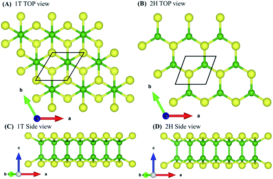 | ||
| Fig. 1 (A) Top view of 1T, (B) side view of 1T phase, (C) top view of 2H, (D) side view of 2H phase. The structure shown has two buckled hexagonal layers arranged in such a way that, in the 2H configuration, boron atoms are located on boron atoms and chalcogen atoms are located at chalcogen atoms, but in the 1T configuration boron atoms are located on boron atoms and chalcogen atoms are placed at the hexagon centers. Green and yellow colors denote boron and chalcogen atoms, respectively. The black box indicates a unit cell containing four atoms. | ||
| System | BS | BSe | BTe | |||
|---|---|---|---|---|---|---|
| Phase | 1T | 2H | 1T | 2H | 1T | 2H |
| a (Å) | 3.06 | 3.04 | 3.27 | 3.26 | 3.59 | 3.57 |
| d B–B (Å) | 1.70 | 1.73 | 1.69 | 1.71 | 1.68 | 1.71 |
| d B–X (Å) | 1.95 | 1.95 | 2.11 | 2.10 | 2.32 | 2.31 |
| d X–X (Å) | 3.81 | 3.43 | 4.02 | 3.61 | 4.28 | 3.83 |
| ∠BBX | 115.45 | 115.83 | 116.22 | 116.71 | 116.51 | 117.21 |
| ∠BXB | 102.89 | 102.44 | 101.94 | 101.34 | 101.61 | 100.74 |
| E coh | −5.79 | −5.78 | −5.24 | −5.23 | −4.72 | −4.69 |
In order to further investigate the stability of the BX (S, Se, Te) monolayer, phonon calculations were performed along the Γ–M–K–Γ high symmetry directions. Fig. S1 (ESI†) shows the obtained phonon dispersion curves, which show good agreement with previous investigations.31 Most of the BX monolayers are free from imaginary frequencies, except BTe (2H). BTe (2H) can be considered dynamically stable and includes very low imaginary frequencies (−0.224 THz) close to Γ, due to numerical anomalies that would be improved if a larger supercell or increased k-points were used for calculation. Since the B atom has a lower mass, it appears to vibrate at high frequencies; hence the higher frequencies associated with optical phonons are contributed by B atoms. Chalcogen atoms contribute so much to vibrations at lower frequencies. There are two frequency gaps observed in the phonon dispersions for all the monolayers, which are due to mass differences between elements B and X (S, Se, Te) and the vibration modes. The calculated phonon dispersion curves also indicate that the 1T phase has slightly higher frequencies than the 2H phase.
The calculated electronic band structures and corresponding densities of states are shown in Fig. 2 and 3. The figures show that the considered materials, boron monochalcogenides BX (X = S, Se, Te), are all broad indirect band gap semiconductors. In all the band structures the top of the valence band arises at the high symmetry point Γ (0, 0, 0) and the minimum of the conduction band occurs very near to the M (0.5, 0, 0) point. The related band gap values of BS (1T), BSe (1T), and BTe (1T) are 2.92 eV, 2.46 eV, and 1.78 eV, respectively. For the 2H phase the band gaps of BS (2H), BSe (2H), and BTe (2H) are 2.83 eV, 2.55 eV, and 1.53 eV, respectively. We observed that the 2H phases have lower bandgap values in comparison with the 1T phases due to the different atomic arrangements. We also noticed that with the increasing size and weight of the chalcogen atoms, the band gap decreases, as shown in Fig. 4(a). We employed the hybrid functional HSE06 to find more accurate electronic band structures, as shown in Fig. S2 (ESI†). The electronic band gaps using HSE06 functional are BS (1T) = 4.03 eV, BS (2H) = 3.91 eV, BSe (1T) = 3.89 eV, BSe (2H) = 3.47 eV, BTe (1T) = 2.48 eV and BTe (2H) = 2.14 eV. Additionally, we calculated the electronic band structure and corresponding electronic density of states due to the presence of heavy atomic weight using PBE functional with spin–orbit coupling effect for both phases of the BTe monolayer, as depicted in Fig. S3 (ESI†). The electronic band gap is affected due to the presence of Te atoms in both the 1T and 2H phases. The computed electronic band gaps of the structure are BTe (1T): Eg = 1.54 eV from 1.78 eV, and BTe (2H): Eg = 1.24 eV from 1.53 eV.
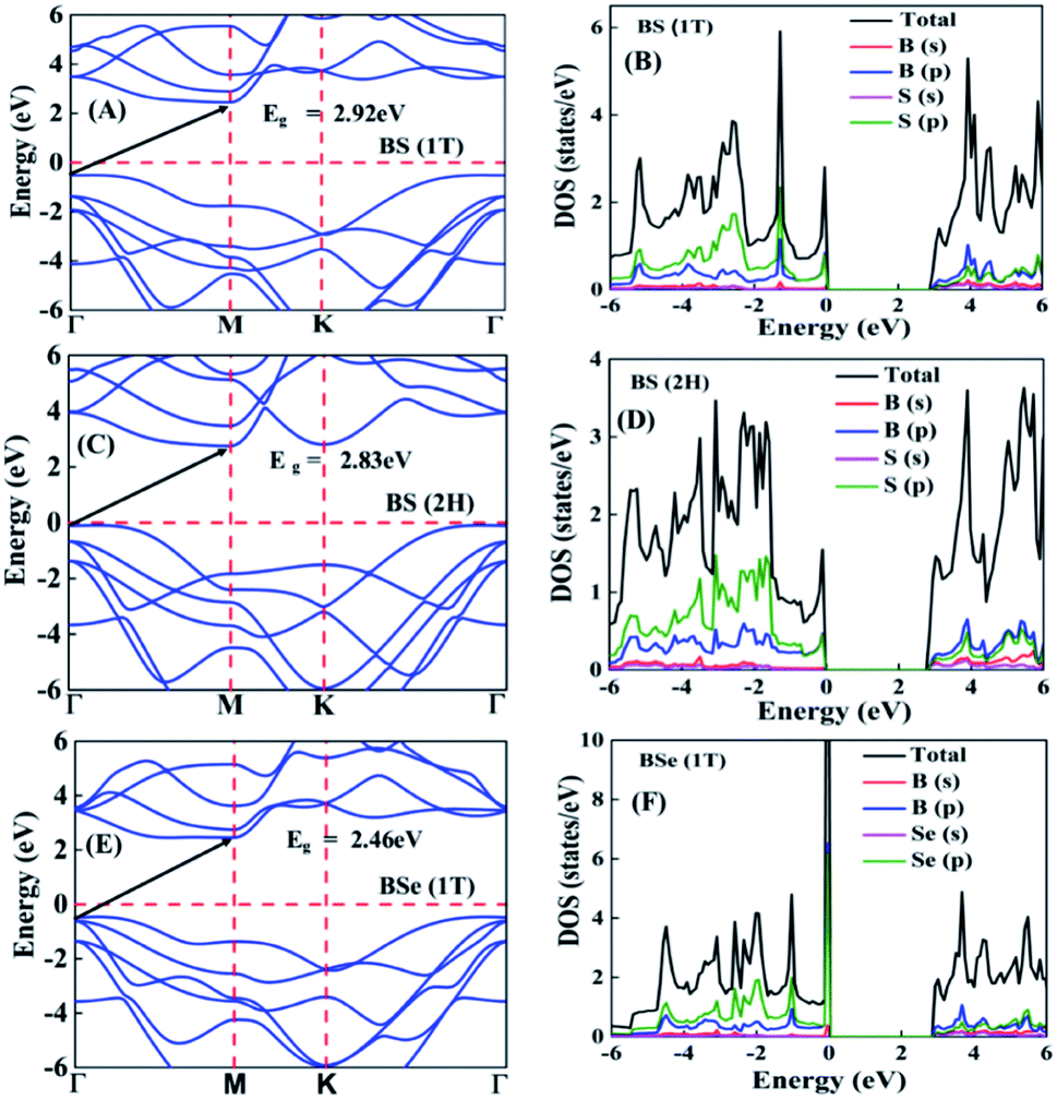 | ||
| Fig. 2 (A) Electronic band structure and (B) corresponding projected density of states of BS 1T phase. (C) Electronic band structure and (D) corresponding projected density of states of BS 2H phase. (E) Electronic band structure and (F) corresponding projected density of states of BSe 1T phase. | ||
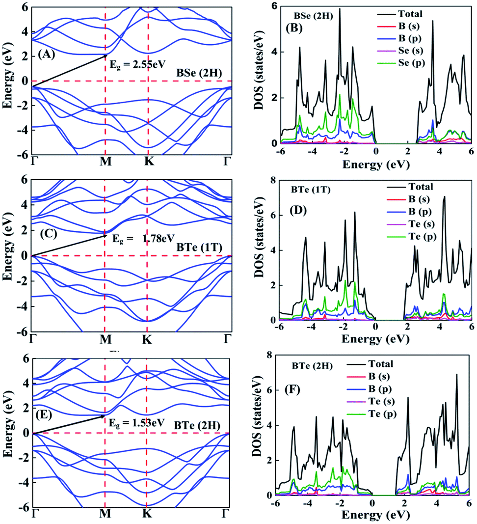 | ||
| Fig. 3 (A) Electronic band structure and (B) corresponding projected density of states of BSe 2H phase. (C) Electronic band structure and (D) corresponding projected density of states of BTe 1T phase. (E) Electronic band structure and (F) corresponding projected density of states of BTe 2H phase. | ||
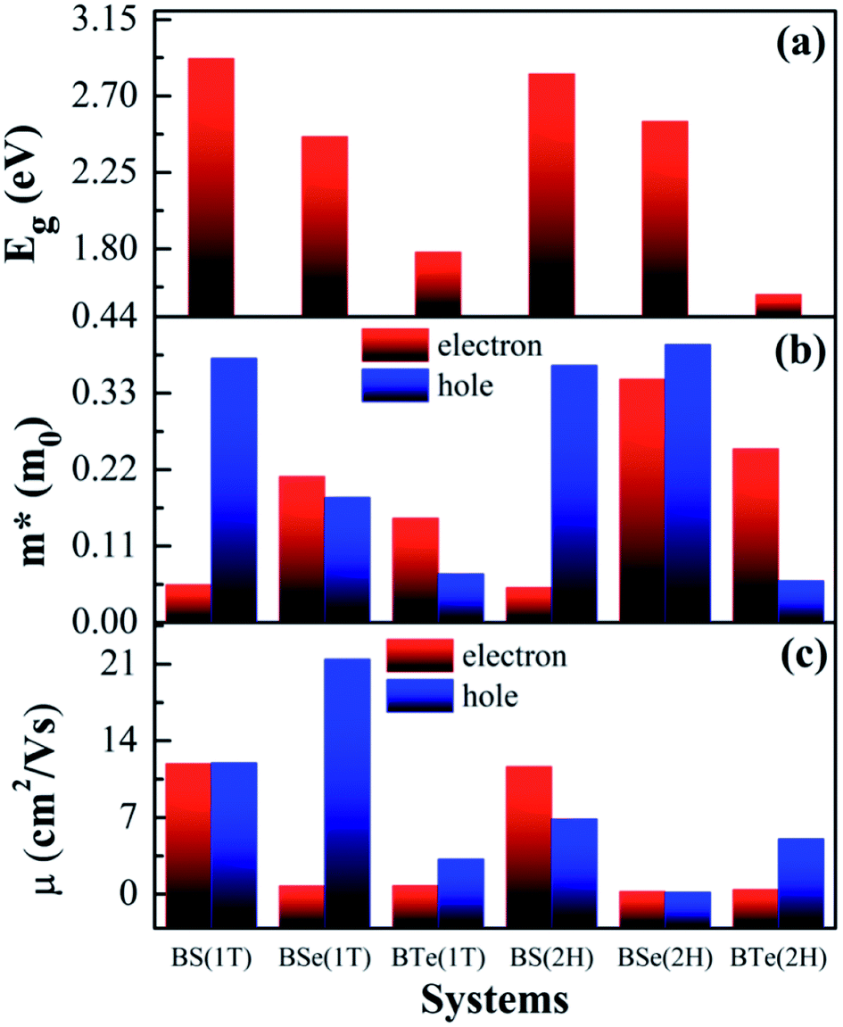 | ||
| Fig. 4 Calculated electronic properties of boron monochalcogenide BX (X = S, Se, Te) monolayer showing (a) the electronic band gap, (b) effective mass of electrons and holes, and (c) carrier mobility (×103) of electrons and holes. | ||
To better understand the electronic structures of BX, we plot the total density of states (TDOS) and projected density of states (PDOS), which are also shown in Fig. 2 and 3. The PDOS provides detailed information about the contribution of different atomic orbitals in the valence band and conduction band of BX (S, Se, Te). The s-orbitals of B and X atoms make a very small contribution to both the valence band and the conduction band. In the valence band away from the Fermi level, the p-orbital of the X atom is dominant over the p-orbital of B, but near the Fermi level the p-orbital of X is hybridized with the 2p-orbital of B atom. In the BS (1T), BS (2H) and BSe (1T) systems, we can see that very near to the Fermi level, the p-orbital of B has a slightly larger contribution than the p-orbitals of S and Se atoms. In the conduction band away from the Fermi level, the 2p-orbital of B is dominant over the p-orbital of X. Abrupt changes in the DOS indicate a high Seebeck coefficient.42,43
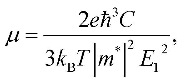
For calculating the relaxation time, we need the carrier mobility (μ). The carrier mobility can be determined by the use of deformation potential (DP) theory suggested by Bardeen and Shockley,44 which is based on effective mass approximation. The carrier mobility is given by the following relation:45–48
 | (2) |
 and E1 is the deformation potential defined as
 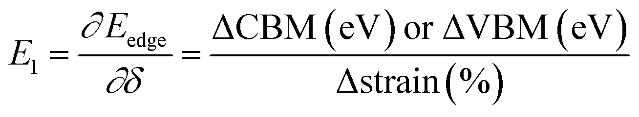 where Eedge for CBM (eV) = conduction band minimum for electrons and Eedge for VBM (eV) = valence band maxima for holes. δ is the % uniaxial strain and is defined as strain (%):
 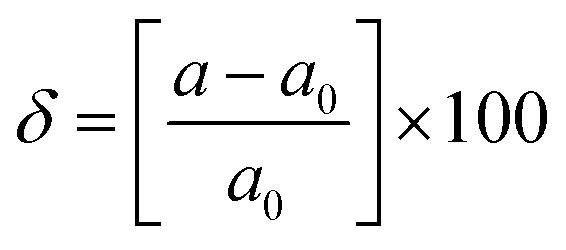 . Here, a0 = lattice constant without strain and a = lattice constant after applying strain. Additionally, we have calculated two E1; the first is for electrons and the second for holes. ΔCBM (eV) = ∂Eedge is the shift in the conduction band minimum upon applying the strain (%) δ. ΔVBM (eV) = ∂Eedge is the shift in the valence band maximum upon applying the strain (%) δ. E1 is determined by linear fitting of the CBM (eV) and VBM (eV) values of Eedge and uniaxial strain in % δ. In this work the range of strain % is taken as −1% to 1%, and at intervals of every 0.2%, we calculated the CBM (eV) and VBM (eV) values of Eedge. A graph was plotted between strain (%) and CBM (eV), as shown in Fig. S5 (ESI†). After linear fitting we measured the slope, that is the value of E1, for further calculation of the mobility and relaxation time of electrons. Similarly, we plotted a graph between strain (%) and VBM (eV), as shown in Fig. S6 (ESI†). After linear fitting we measured the slope, that is the value of E1, for further calculation of the mobility and relaxation time for holes. The electron/hole relaxation time can be determined by τ = μm*/e.
The calculated effective mass of the carriers (electrons and holes) is shown in Tables 2 and 3. The values of electron effective mass are significantly lower in the BS monolayer (both phases) as compared to the BSe and BTe monolayers, as shown in Fig. 4(b). The effective masses of carriers for electrons in the 1T and 2H phases of boron monochalcogenide BX (X = S, Se, Te) monolayers are comparable to the values for phosphorene,47 CP 45,49 and hexagonal M2C3 (M = As, Sb, and Bi) monolayers.50 We also calculated the carrier mobility at room temperature (T = 300 K) using eqn (2), as presented in Table 2. Due to the small effective mass, the BS monolayer has a high electron carrier mobility of 1.19 × 104 cm2 V−1 s−1 for the 1T phase and 1.16 × 104 cm2 V−1 s−1 for the 2H phase, which is significantly larger than monolayer MoS2.51 The hole carrier mobilities of 1.198 × 104 cm2 V−1 s−1 for BS (1T phase) and 2.14 × 104 cm2 V−1 s−1 for BSe (1T phase) are slightly larger than the electron carrier mobilities. Additionally, the BSe and BTe monolayers with 1T and 2H phases have slightly lower electron mobilities in the order of 102 cm2 V−1 s−1 because they have a higher effective mass, as presented in Fig. 4. Fig. 4(c) depicts a comparison of the carrier mobilities for electrons and holes in boron monochalcogenide BX (X = S, Se, Te) monolayers. A higher carrier mobility enhances the electronic conductivity because both carrier mobility (μ) and electronic conductivity are directly proportional to relaxation time (τ). According to this, the thermoelectric figure of merit (ZT) depends on carrier mobility and other parameters such as thermal conductivity and the Seebeck coefficient.
| System | E 1 (eV) | C (N m−1) | m* (m0) | μ (cm2 V−1 s−1) | τ (fs) |
|---|---|---|---|---|---|
| BS (1T) | 11.24 | 205.078 | 0.054 | 11903.07 |
243.71 |
| BS (2H) | 12.66 | 218.340 | 0.050 | 11651.61 |
220.89 |
| BSe (1T) | 10.36 | 166.857 | 0.210 | 753.78 | 60.01 |
| BSe (2H) | 11.14 | 178.182 | 0.350 | 250.62 | 33.26 |
| BTe (1T) | 10.23 | 129.395 | 0.150 | 783.34 | 66.83 |
| BTe (2H) | 10.83 | 142.559 | 0.250 | 415.83 | 39.41 |
| System | E 1 (eV) | C (N m−1) | m* (m0) | μ (cm2 V−1 s−1) | τ (fs) |
|---|---|---|---|---|---|
| BS (1T) | 1.30 | 205.078 | 0.38 | 11979.37 |
2589.04 |
| BS (2H) | 1.82 | 218.340 | 0.37 | 6863.66 | 1444.93 |
| BSe (1T) | 1.85 | 166.857 | 0.18 | 21449.88 |
2195.93 |
| BSe (2H) | 9.70 | 178.182 | 0.40 | 168.72 | 38.38 |
| BTe (1T) | 10.84 | 129.395 | 0.07 | 3197.65 | 127.31 |
| BTe (2H) | 10.57 | 142.559 | 0.06 | 5052.56 | 172.41 |
3.2 Thermoelectric properties
In this section, to analyze the thermoelectric properties of materials, we calculated the electronic thermal conductivity (κe/τ), electric conductivity (σ/τ), Seebeck coefficient (S) and figure of merit (ZT). Fig. 5(A) illustrates the relation between electronic thermal conductivity (κe/τ) and temperature. Lattice vibrations and electron motion are accountable for thermal conductivity. The part of thermal conductivity which arises due to the motion of electrons is considered electronic thermal conductivity. For BS (1T), the electronic thermal conductivity is much less at room temperature; it is 4.99 × 10⁷ W m−1 K−1 s−1 at 300 K and increases with increasing temperature, reaching 1.77 × 10¹³ W m−1 K−1 s−1 at 1000 K. The electronic thermal conductivity of all the other materials increases significantly with increasing temperature. The calculated data is given in Table 4.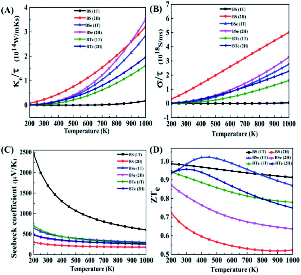 | ||
| Fig. 5 (A) Electronic thermal conductivity (κe/τ), (B) electric conductivity (σe/τ), (C) Seebeck coefficient (S), and (D) figure of merit (ZT) of the thermoelectric properties of 2D boron monochalcogenide BX (X = S, Se, Te) monolayer. | ||
| Materials | Phase | κ e/τ, 1014 W m−1 K−1 s−1 | |
|---|---|---|---|
| 300 K | 1000 K | ||
| BS | 1T | ||
| BS | 2H | 0.233 | 3.21 |
| BSe | 1T | 0.050 | 2.85 |
| BSe | 2H | 0.064 | 3.51 |
| BTe | 1T | 0.025 | 1.62 |
| BTe | 2H | 0.063 | 1.96 |
From the above data we establish that the 2H phase has more electronic thermal conductivity as compared to the 1T phase, and in the 2H phase the electronic thermal conductivity increases more rapidly than in the 1T phase. BS (2H) phase has the highest value of electronic thermal conductivity, 0.233 × 10¹⁴ W m−1 K−1 s−1 at 300 K. On the other hand, at 1000 K the BSe (2H) maximum value is 3.51 × 10¹⁴ W m−1 K−1 s−1, since BSe (2H) shows a larger temperature gradient near 900 K. At 900 K BS (2H) has 2.59 × 10¹⁴ W m−1 K−1 s−1 electronic thermal conductivity, while BSe (2H) has 2.61 × 10¹⁴ W m−1 K−1 s−1. Low thermal conductivity materials are needed for high performance thermoelectric devices.
Fig. 5(B) shows the graph of electric conductivity (σ/τ) versus temperature. In the BS (1T) phase electric conductivity (σ/τ) is also very low, similar to the electronic thermal conductivity (κe/τ). At 300 K it is only 5.72 × 10¹⁰ S ms−1; it increases with increasing temperature and reaches 4.42 × 10¹⁶ S ms−1 at 1000 K. Beside this, all the other materials have more incremental electric conductivity, which is visible in the graph. The calculated data is presented in Table 5.
| Materials | Phase | σ/τ, 1018 S ms−1 | |
|---|---|---|---|
| 300 K | 1000 K | ||
| BS | 1T | ||
| BS | 2H | 0.808 | 5.02 |
| BSe | 1T | 0.064 | 2.77 |
| BSe | 2H | 0.158 | 3.27 |
| BTe | 1T | 0.027 | 1.62 |
| BTe | 2H | 0.124 | 2.27 |
A similar trend is seen here; the 2H phases of all materials possess more electric conductivity than the 1T phases. The rate of increase of electric conductivity with temperature is greater in the 2H phase than in the 1T phase. In the case of BS (2H), electric conductivity increased approximately linearly with temperature and reached 5.02 × 10¹⁸ S ms−1. High electric conductivity is needed for good thermoelectric devices.
Fig. 5(C) shows the graph of Seebeck coefficient versus temperature. It is clear from the graph that the Seebeck coefficient decreases as the temperature increases. BS (1T) shows something amazing here – a very high Seebeck coefficient of 2460 μV K−1 at 200 K, which is higher than that reported for cubic phase SnSe in an earlier study,52 and 1690 μV K−1 at room temperature (300 K). After 500 K it decreases rapidly to reach 605.87 μV K−1 at 1000 K, while so much drastic change is not observed in the other materials. The positive Seebeck coefficient for BS (1T) shows that this is a p-type semiconductor. Therefore, the upper part of the valence band has the greatest influence on the electric properties of the material. As shown in Fig. 2(A) in the dispersion of band structure near valence band maxima (VBM), along the Γ–M line, the curves are nearly flat, showing a high carrier (hole) effective mass around VBM. These bands are also known as heavy bands. Previous research has shown that heavy bands provide high Seebeck coefficients.42,53–55
The calculated data for the Seebeck coefficient is shown in Table 6. From the above data, we can see that BS (2H) has the smallest Seebeck coefficient among all the materials. The 1T phases of the materials provide larger Seebeck coefficients than the 2H phases. High Seebeck coefficients are needed for high performance thermoelectric devices.
| Materials | Phase | S, (μV K−1) | |
|---|---|---|---|
| 300 K | 1000 K | ||
| BS | 1T | ||
| BS | 2H | 248.87 | 182.94 |
| BSe | 1T | 506.65 | 299.05 |
| BSe | 2H | 387.77 | 261.44 |
| BTe | 1T | 531.15 | 279.29 |
| BTe | 2H | 401.02 | 254.62 |
Fig. 5(D) illustrates the variation in the electronic figure of merit (ZTe) with temperature. For some materials (BSe 1T and BTe 2H), the electronic figure of merit (ZTe) increases with an increase in temperature; after reaching a maximum value it starts to decrease, but for all the other materials it decreases with increasing temperature. The calculated data for different temperatures is given in Table 7.
| System | ZT e | ||||||
|---|---|---|---|---|---|---|---|
| T | 200 K | 250 K | 300 K | 350 K | 400 K | 450 K | 1000 K |
| BS (1T) | 0.99 | 0.99 | 0.97 | 0.97 | 0.97 | 0.96 | 0.91 |
| BS (2H) | 0.72 | 0.68 | 0.64 | 0.62 | 0.60 | 0.60 | 0.52 |
| BSe (1T) | 0.94 | 0.96 | 0.98 | 1.01 | 1.02 | 1.02 | 0.87 |
| BSe (2H) | 0.87 | 0.84 | 0.81 | 0.79 | 0.76 | 0.74 | 0.63 |
| BTe (1T) | 0.94 | 0.93 | 0.91 | 0.90 | 0.89 | 0.87 | 0.78 |
| BTe (2H) | 0.94 | 0.95 | 0.96 | 0.95 | 0.94 | 0.92 | 0.75 |
From the above data, at low temperature and near room temperature ZTe is about 0.7 to 1.0 for all the materials except BS (2H). Therefore, the remaining five materials can be considered good thermoelectric materials at low temperature and near room temperature. Of all of them, BSe (1T) is the best thermoelectric material, having the highest ZTe of 1.022 at 450 K temperature.
4 Conclusion
We have systematically investigated the electronic, vibrational and thermoelectric properties of boron monochalcogenide BX (X = S, Se, Te) materials using a density functional theory framework. The computed cohesive energy of each phase of boron monochalcogenides has a negative value, which shows the stability of the materials. From the phonon band structure calculations, the positive phonon frequencies show the dynamic stability of the materials. The electronic band structure shows that each material has an indirect bandgap varying from 2.92 eV to 1.53 eV. Due to the presence of the small effective mass of electrons, boron monochalcogenide BX (X = S, Se, Te) materials have superior carrier mobility. The 1T and 2H phases of the BS monolayer have carrier mobilities of 1.19 × 10⁴ and 1.16 × 104 cm2 V−1 s−1. From the thermoelectric calculations, we found that for the low and mid-temperature range of 200 K to 450 K, each phase of the boron monochalcogenides shows a high electronic figure of merit ZTe nearly equal to 1, with the exception of the BS 2H phase. The 1T phase of the BSe monolayer has the highest ZTe = 1.022, which is the maximum across all the studied materials. These findings suggest that boron monochalcogenide monolayer materials have great potential applications in the field of high-performance thermoelectric devices.Conflicts of interest
There are no conflicts to declare.Acknowledgements
P. M. is thankful to SVNIT, Surat, for his Institute Research fellowship (FIR-DS17PH004). D. S. and R. A. thank Olle Engkvists Stiftelse, Carl Tryggers Stiftelse för Vetenskaplig Forskning (CTS) and Swedish Research Council (VR) for financial support. SNIC and HPC2N are acknowledged for providing the computing facilities. Y. A. S. is thankful to the Science and Engineering Research Board (SERB), India, for the financial support (grant number: EEQ/2016/000217).References
- T. M. Tritt and M. Subramanian, MRS Bull., 2006, 31, 188–198 CrossRef.
- K. Biswas, J. He, I. D. Blum, C.-I. Wu, T. P. Hogan, D. N. Seidman, V. P. Dravid and M. G. Kanatzidis, Nature, 2012, 489, 414 CrossRef CAS PubMed.
- M. S. Dresselhaus, G. Chen, M. Y. Tang, R. Yang, H. Lee, D. Wang, Z. Ren, J.-P. Fleurial and P. Gogna, Adv. Mater., 2007, 19, 1043–1053 CrossRef CAS.
- G. J. Snyder and E. S. Toberer, Materials for sustainable energy: a collection of peer-reviewed research and review articles from Nature Publishing Group, World Scientific, 2011, pp. 101–110 Search PubMed.
- H. Wang, Y. Pei, A. D. LaLonde and G. J. Snyder, Adv. Mater., 2011, 23, 1366–1370 CrossRef CAS PubMed.
- L. E. Bell, Science, 2008, 321, 1457–1461 CrossRef CAS PubMed.
- W. G. Zeier, J. Schmitt, G. Hautier, U. Aydemir, Z. M. Gibbs, C. Felser and G. J. Snyder, Nat. Rev. Mater., 2016, 1, 16032 CrossRef CAS.
- D. Singh, S. Kansara, S. K. Gupta and Y. Sonvane, J. Mater. Sci., 2018, 53, 8314–8327 CrossRef CAS.
- L. Hicks and M. S. Dresselhaus, Phys. Rev. B: Condens. Matter Mater. Phys., 1993, 47, 12727 CrossRef CAS PubMed.
- J. P. Heremans, V. Jovovic, E. S. Toberer, A. Saramat, K. Kurosaki, A. Charoenphakdee, S. Yamanaka and G. J. Snyder, Science, 2008, 321, 554–557 CrossRef CAS PubMed.
- Y. Pei, X. Shi, A. LaLonde, H. Wang, L. Chen and G. J. Snyder, Nature, 2011, 473, 66 CrossRef CAS PubMed.
- Y. Pei, A. LaLonde, H. Wang and G. J. Snyder, Energy Environ. Sci., 2012, 5, 7963 RSC.
- D. Singh and R. Ahuja, ACS Appl. Energy Mater., 2019, 2, 6891–6903 CrossRef CAS.
- J. Yu, K. Xia, X. Zhao and T. Zhu, J. Phys. D: Appl. Phys., 2018, 51, 113001 CrossRef.
- N. P. Blake, S. Latturner, J. D. Bryan, G. D. Stucky and H. Metiu, J. Chem. Phys., 2001, 115, 8060–8073 CrossRef CAS.
- H. R. Aliabad, M. Ghazanfari, I. Ahmad and M. Saeed, Comput. Mater. Sci., 2012, 65, 509–519 CrossRef.
- A. Weidenkaff, M. Aguirre, L. Bocher, M. Trottmann, P. Tomes and R. Robert, J. Korean Ceram. Soc., 2010, 47, 47–53 CrossRef CAS.
- M. Bilal, B. Khan, H. R. Aliabad, M. Maqbool, S. J. Asadabadi and I. Ahmad, Comput. Phys. Commun., 2014, 185, 1394–1398 CrossRef CAS.
- I. Matsubara, R. Funahashi, T. Takeuchi, S. Sodeoka, T. Shimizu and K. Ueno, Appl. Phys. Lett., 2001, 78, 3627–3629 CrossRef CAS.
- W. Shin, N. Murayama, K. Ikeda and S. Sago, J. Power Sources, 2001, 103, 80–85 CrossRef CAS.
- X. Wang, R. Yang, Y. Zhang, P. Zhang and Y. Xue, Appl. Phys. Lett., 2011, 98, 222110 CrossRef.
- K. Pandey, P. Yadav, D. Singh, S. K. Gupta, Y. Sonvane, I. Lukačević, J. Kim and M. Kumar, Sci. Rep., 2016, 6, 32690 CrossRef CAS PubMed.
- V. Sousa, Microelectron. Eng., 2011, 88, 807–813 CrossRef CAS.
- S. LeBlanc, Sustainable Mater. Technol., 2014, 1–2, 26–35 CrossRef.
- C. Xiao, X. Qin, J. Zhang, R. An, J. Xu, K. Li, B. Cao, J. Yang, B. Ye and Y. Xie, J. Am. Chem. Soc., 2012, 134, 18460–18466 CrossRef CAS.
- T.-R. Wei, Y. Qin, T. Deng, Q. Song, B. Jiang, R. Liu, P. Qiu, X. Shi and L. Chen, Sci. China Mater., 2019, 62, 8–24 CrossRef CAS.
- S. Li, X. Li, Z. Ren and Q. Zhang, J. Mater. Chem. A, 2018, 6, 2432–2448 RSC.
- X. Chen, Y. Huang, J. Liu, H. Yuan and H. Chen, ACS Omega, 2019, 4, 17773–17781 CrossRef CAS PubMed.
- M.-S. Li, K.-X. Chen, D.-C. Mo and S.-S. Lyu, Phys. Chem. Chem. Phys., 2019, 21, 24695–24701 RSC.
- N. T. Hung, A. R. Nugraha and R. Saito, Appl. Phys. Lett., 2017, 111, 092107 CrossRef.
- B. Mortazavi and T. Rabczuk, Energies, 2018, 11, 1573 CrossRef.
- G. Kresse and D. Joubert, Phys. Rev. B: Condens. Matter Mater. Phys., 1999, 59, 1758 CrossRef CAS.
- G. Kresse and J. Furthmüller, Comput. Mater. Sci., 1996, 6, 15–50 CrossRef CAS.
- G. Kresse and J. Furthmüller, Phys. Rev. B: Condens. Matter Mater. Phys., 1996, 54, 11169 CrossRef CAS PubMed.
- J. P. Perdew, K. Burke and M. Ernzerhof, Phys. Rev. Lett., 1996, 77, 3865 CrossRef CAS PubMed.
- H. J. Monkhorst and J. D. Pack, Phys. Rev. B: Solid State, 1976, 13, 5188 CrossRef.
- A. Togo and I. Tanaka, Scr. Mater., 2015, 108, 1–5 CrossRef CAS.
- G. K. Madsen and D. J. Singh, Comput. Phys. Commun., 2006, 175, 67–71 CrossRef CAS.
- B. Qiu, Z. Tian, A. Vallabhaneni, B. Liao, J. M. Mendoza, O. D. Restrepo, X. Ruan and G. Chen, EPL, 2015, 109, 57006 CrossRef.
- J. Sun and D. J. Singh, Phys. Rev. Appl., 2016, 5, 024006 CrossRef.
- K. Momma and F. Izumi, J. Appl. Crystallogr., 2011, 44, 1272–1276 CrossRef CAS.
- D. Zou, S. Xie, Y. Liu, J. Lin and J. Li, J. Mater. Chem. A, 2013, 1, 8888–8896 RSC.
- M.-S. Lee, F. P. Poudeu and S. Mahanti, Phys. Rev. B: Condens. Matter Mater. Phys., 2011, 83, 085204 CrossRef.
- J. Bardeen and W. Shockley, Phys. Rev., 1950, 80, 72 CrossRef.
- G. Wang, R. Pandey and S. P. Karna, Nanoscale, 2016, 8, 8819–8825 RSC.
- D. Singh, S. K. Gupta, Y. Sonvane, T. Hussain and R. Ahuja, Phys. Chem. Chem. Phys., 2018, 20, 21716–21723 RSC.
- R. Fei and L. Yang, Nano Lett., 2014, 14, 2884–2889 CrossRef CAS PubMed.
- S. Bruzzone and G. Fiori, Appl. Phys. Lett., 2011, 99, 222108 CrossRef.
- D. Singh, V. Shukla, P. K. Panda, Y. K. Mishra, H.-G. Rubahn and R. Ahuja, New J. Chem., 2020, 44, 3777–3785 RSC.
- P.-F. Liu, T. Bo, Z. Liu, O. Eriksson, F. Wang, J. Zhao and B.-T. Wang, J. Mater. Chem. C, 2018, 6, 12689–12697 RSC.
- B. Radisavljevic, A. Radenovic, J. Brivio, V. Giacometti and A. Kis, Nat. Nanotechnol., 2011, 6, 147 CrossRef CAS PubMed.
- F. K. Butt, B. U. Haq, S. ur Rehman, R. Ahmed, C. Cao and S. AlFaifi, J. Alloys Compd., 2017, 715, 438–444 CrossRef CAS.
- J. Ding, B. Xu, Y. Lin, C. Nan and W. Liu, New J. Phys., 2015, 17, 083012 CrossRef.
- K. Kaur, EPL, 2017, 117, 47002 CrossRef.
- S.-D. Guo, RSC Adv., 2016, 6, 47953–47958 RSC.
Footnote |
| † Electronic supplementary information (ESI) available. See DOI: 10.1039/d0se00004c |
| This journal is © The Royal Society of Chemistry 2020 |