
Surface passivation via acid vapor etching enables efficient and stable solution-processed CdTe nanocrystal solar cells†
Xiuzhen
Guo‡
ac,
Zhitao
Rong‡
ac,
Le
Wang
b,
Songwei
Liu
ac,
Zhe
Liu
 b,
Kaiying
Luo
ac,
Bingchang
Chen
ac,
Donghuan
Qin
*ac,
Yuguang
Ma
ac,
Hongbin
Wu
ac and
Lintao
Hou
*b
b,
Kaiying
Luo
ac,
Bingchang
Chen
ac,
Donghuan
Qin
*ac,
Yuguang
Ma
ac,
Hongbin
Wu
ac and
Lintao
Hou
*b
aInstitute of Polymer Optoelectronic Materials & Devices, State Key Laboratory of Luminescent Materials & Devices, South China University of Technology, Guangzhou 510640, China. E-mail: qindh@scut.edu.cn
bDepartment of Physics, Guangdong Provincial Key Laboratory of Optical Fiber Sensing and Communications, Guangzhou Key Laboratory of Vacuum Coating Technologies and New Energy Materials, Siyuan Laboratory, Jinan University, Guangzhou 510632, China. E-mail: thlt@jnu.edu.cn
cSchool of Materials Science and Engineering, South China University of Technology, Guangzhou 510640, China
First published on 4th November 2019
Abstract
Achieving stable and low-resistance interfaces for hole transport layers with well-matched energy levels is crucial to maximize the performance of solution-processed CdTe nanocrystal (NC) based solar cells. Wet chemical etching with substrates immersed in dilute acid solutions is commonly adopted to modify traditional thick vacuum-evaporated CdTe layers for forming a conductive layer with good ohmic contact with the metal electrode. However, for next-generation low-cost solution-processed CdTe NC based solar cells, this method has failed so far since the acid (Br2/CH3OH or HNO3/H3PO4) can permeate easily into the grain boundaries of CdTe NCs and form a device shunt. Herein, a new technology called acid vapor etching (AVE) is developed for the first time for solution-processed CdTe NC solar cells. It's found that surface passivation can be well controlled during a mild bromine–methanol (BM) vapor etching process. Besides BM, other acid solutions such as a nitric–acetic (NA) acid solution are also suitable to adjust the CdTe interface, illustrating the remarkable universality of this method. The AVE-processed devices with an inverted configuration of ITO/ZnO/CdSe/CdTe/Au show very high efficiencies of 8.38% (BM) and 8.67% (NA) due to significant enhancement in short-circuit current, which are increased by ∼30% over that of a conventional device (5.83%) without AVE. Moreover, the AVE-processed CdTe NC solar cells show a striking improvement in stability, indicating their potential application in the manufacture of large-area solution-processed CdTe solar cells.
Introduction
Since CdTe is a narrow direct band gap (1.45 eV) semiconductor with a high absorption coefficient (up to 105 cm−1) in the visible light range,1–4 which enables the absorption of 95% photons within a ∼1 μm thick active layer, it is generally regarded as one of the commercially promising materials in the field of solar cells. However, the high work function (∼5.7 eV) and high resistance of CdTe thin films limit the efficiency improvement of CdTe NC solar cells, since there is no such high-work-function metal or alloy to achieve good ohmic contact with p-type CdTe.5–8 As a result, high-efficiency CdTe solar cells with an inverted configuration are typically adopted with the introduction of a hole transport layer (HTL) before the deposition of the metal electrode. For example, HTLs of Sb2Te3, ZnTe, NiO or WO3 are often employed in inverted CdTe solar cells.9–12 In lots of hole transport alternatives, use of Cu-doped CdTe as a back-contact interface layer is one of the most successful approaches to eliminate the energy barrier between p-type CdTe and the metal electrode in CdTe solar cells.13–15 It is stated that Cu-doping can create shallow energy levels for CdTe thin films, which is advantageous to reduce back-contact resistance. However, Cu may also diffuse into the p–n junction with the formation of trap recombination centers, which negatively affects the long-term stability of CdTe solar cells under high-temperature and high-humidity storage.16 For solving this problem, wet chemical etching (WCE) is generally utilized to optimize the CdTe/Au interface. Bromine–methanol (BM), HNO3/H3PO4 acid (NP) and K2Cr2O7–H2SO4 have usually been employed as etching solutions in WCE for traditional CdTe thin film solar cells prepared by close-space sublimation (CSS) or other vacuum techniques.17–19 However, there have been no successful reports of the WCE technology being applied in low-cost solution-processed CdTe NC solar cells to date.For solution printable CdTe NC solar cells with an inverted structure, a feasible practice is that a HTL is inserted between the active layer and high-valence-band CdTe to reduce the charge injection/extraction barrier. For instance, Yang and co-workers demonstrated an effective approach to improve the charge carrier transport and collection by using organic conjugated polymers such as P3KT or spiro-OMeTAD as HTLs for forming an interfacial dipole layer.20,21 Inspired by the application of MoOx in organic solar cells, solution-processed CdTe NC solar cells with MoOx back-contacts were also demonstrated.22 Recently, a novel crosslinkable conjugated polymer, Si-TPA, has been successfully employed in solution-processed CdTe NC solar cells.23 However, most of the devices suffered from instability of HTLs, leading to tremendous efficiency degradation. On the other hand, the carrier concentration of a pristine CdTe NC film is only about 1015 cm−3,24 which also implies the difficulty in achieving superior ohmic behavior between CdTe and the metal-electrode (1023 cm−3) in the absence of interface modification. Although WCE offers great potential for solving the interfacial issue in traditional CSS/vacuum-processed compact CdTe solar cells, it is not suitable for the low-cost solution-processed CdTe NC films for building p+-doped regions since excessive etching could easily occur in the void grain boundaries of non-compact and ultrathin CdTe NC films, making the devices shunt or peel off from the substrates.24 Therefore, it is necessary to develop a new acid etching method which is fully compatible with the low-cost solution-processed CdTe NC solar devices.
Herein, we develop a novel modified chemical etching strategy, which is called acid vapor etching (AVE) for solution-processed CdTe NC solar cells. With the use of this approach, the interface etching of a CdTe NC thin film is well controlled and a Te-rich layer is successfully formed, which is verified by scanning electron microscopy (SEM), atomic force microscopy (AFM), X-ray photoelectron spectroscopy (XPS) and transient photovoltage (TPV). As a result, low trap density and improved minority carrier lifetime in the device are achieved via AVE processing. The solution-processed CdTe NC solar cells with an inverted structure of ITO/ZnO/CdSe/CdTe/Au exhibit high and stable power conversion efficiencies (PCEs) of 8.38% with bromine–methanol (BM) AVE and 8.67% with nitric–acetic acid (NA) AVE, which are increased by more than 30% compared to the control device (5.85%) without AVE. To the best of our knowledge, this is the highest PCE among inverted CdTe NC based solar cells reported to date. This work opens up a novel modification route for developing high-performance printable CdTe NC based solar cells.
Experimental
Materials and precursor solutions
Bromine (Br2), anhydrous methanol (CH3OH), acetic acid (CH3COOH), and nitric acid (HNO3, 69%) were purchased from Guangzhou Chemical Reagent Factory, China. All other chemicals and solvents were used as received. The ZnO precursor, CdSe NCs and CdTe NCs were synthesized based on previous reports.25,26AVE processing and device fabrication
The ITO/ZnO/CdSe/CdTe samples were fabricated through layer-by-layer solution-processing. Commercial ITO-coated glass substrates were washed with acetone, deionized water, and ethanol in sequence. Then ∼40 nm ZnO, ∼60 nm CdSe NC and 500–600 nm CdTe NC films were deposited on the ITO substrate as reported previously.27,28 The ZnO layer was coated on the ITO substrate, serving as an electron transfer layer for reducing interface recombination. Two layers of CdSe NCs (∼60 nm) and five layers of CdTe NCs (∼500 nm) were then deposited on the ITO/ZnO as the p–n junction. All the CdTe NC thin films were annealed at 340 °C with CdCl2 treatment for 30 min.Then BM or NA solutions with different concentrations were used as acid vapor etching solutions for CdTe NC thin films. The optimal BM solution contains a volume ratio of V(bromine)![[thin space (1/6-em)]](https://www.rsc.org/images/entities/char_2009.gif) :V(methanol) = 1:2000, while V(nitric acid):V(acetic acid):V(methanol) is 3:80:400 for the optimal NA solution. For example, the BM solution is made of 20 μL liquid bromine, 40 mL anhydrous methanol and 1 mL deionized water, and the NA solution is composed of 300 μL HNO3, 8 mL acetic acid (98% wt) and 40 mL anhydrous methanol. Fig. 1 shows the schematic illustration of the AVE method for CdTe NC thin films. In a fume hood, the prepared ITO/ZnO/CdSe/CdTe samples are placed in a shadow mask which is mounted on an iron support stand. The surface of CdTe films is faced down towards the acid etching solution. The distance between CdTe samples and the acid solution is ∼10 cm. Firstly, the acid solution is heated up to 65 °C and kept at this temperature for 10 min to obtain stable acid volatilization. Then the ITO/ZnO/CdSe/CdTe samples are transferred into the acid vapor for different etching times. After chemical vapor etching, the samples are rinsed with anhydrous methanol and dried with nitrogen. Finally, 80 nm Au is thermally deposited on ITO/ZnO/CdSe/CdTe samples through a shallow mask. The active area of NC solar cells is 0.08 cm2.
:V(methanol) = 1:2000, while V(nitric acid):V(acetic acid):V(methanol) is 3:80:400 for the optimal NA solution. For example, the BM solution is made of 20 μL liquid bromine, 40 mL anhydrous methanol and 1 mL deionized water, and the NA solution is composed of 300 μL HNO3, 8 mL acetic acid (98% wt) and 40 mL anhydrous methanol. Fig. 1 shows the schematic illustration of the AVE method for CdTe NC thin films. In a fume hood, the prepared ITO/ZnO/CdSe/CdTe samples are placed in a shadow mask which is mounted on an iron support stand. The surface of CdTe films is faced down towards the acid etching solution. The distance between CdTe samples and the acid solution is ∼10 cm. Firstly, the acid solution is heated up to 65 °C and kept at this temperature for 10 min to obtain stable acid volatilization. Then the ITO/ZnO/CdSe/CdTe samples are transferred into the acid vapor for different etching times. After chemical vapor etching, the samples are rinsed with anhydrous methanol and dried with nitrogen. Finally, 80 nm Au is thermally deposited on ITO/ZnO/CdSe/CdTe samples through a shallow mask. The active area of NC solar cells is 0.08 cm2.
 | ||
| Fig. 1 The schematic diagram of the AVE process for solution-processed CdTe NC thin films. | ||
Characteristics
X-ray photoelectron spectroscopy (XPS) spectra were measured using Thermo Fisher Scientific's K-ALPHA+, equipped with a low energy electron–ion binding system. The surface morphology and roughness images were obtained using BRUKER OPTICS' scanning electron microscope (SEM) and atomic force microscope (AFM) in tapping mode, respectively. Current–voltage characteristics (J–V) were obtained with or without irradiation from an AM 1.5G solar simulator at room temperature (Keithley Source Meter, 2400). External quantum efficiency (EQE) measurements were recorded utilizing a QE-R spectral response testing system. The transient photovoltage (TPV) was measured with a Paios system. The electrochemical impedance spectra (EIS) were obtained with KEYSIGHT's E4990A impedance analyzer.Results and discussion
In order to investigate the effect of etching time on the morphologies of CdTe NC thin films, the ITO/ZnO/CdSe/CdTe samples are exposed to the BM vapor for different times (0 s, 30 s, 60 s, 90 s and 120 s) in comparison with the sample treated by the conventional method, viz. dipping the sample into BM solution for 3 s. The process of morphological change for CdTe samples with or without (w/o) AVE is illustrated in Fig. 2. It is shown that the CdTe surface without any etching treatment is smooth with only some small particles at the grain boundaries (Fig. 2a). With the increase of the AVE time, the large grains are split into many corroded grains, which implies that the surface of CdTe has reacted with the acid vapor (Fig. 2b–e). The corroded grains are homogeneous on the whole thin film, suggesting a mild and well-controlled etching process with the AVE strategy. In contrast, there are a lot of pin-holes for the control sample treated under the conventional WCE method (Fig. 2f). Therefore, the conventional WCE method may lead to device shunting, which is not feasible for CdTe NC solar cells. Moreover, as seen from AFM images (Fig. S1†), the surface of ITO/ZnO/CdSe/CdTe films becomes increasingly smooth via AVE treatment with root mean square (RMS) values of 10.7 nm (0 s), 9.78 nm (30 s), 7.29 nm (60 s), 7.26 nm (90 s) and 6.72 nm (120 s). The smooth CdTe NC active layer is beneficial for decreasing interface recombination and increasing carrier collection efficiency. The CdTe films with NA AVE also show similar morphological regularity compared with BM-processed films (Fig. S2†), verifying the universality of this method for achieving high quality CdTe NC films.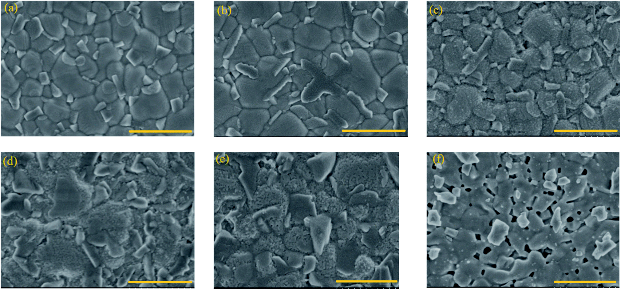 | ||
| Fig. 2 SEM images of solution-processed CdTe thin films (a) without AVE, and with BM AVE for (b) 30 s, (c) 60 s, (d) 90 s and (e) 120 s. (f) SEM image of a solution-processed CdTe thin film dipped in BM solution for 3 s (scale bar = 500 nm). | ||
The chemical binding energy of the CdTe NC thin film w/o acid vapor etching (taking BM as an example) is further investigated by XPS. In order to clarify the content change of CdTe NC thin films w/o AVE, all spectra are calibrated using the carbon C 1s core level as a reference (binding energy at 284.8 eV) before the spectral recording. The Cd/Te atomic ratios are listed in Table 1 and the XPS full-scan spectra are shown in Fig. S3.† It can be found that the 3d peaks of both cadmium and tellurium are split into the 3d5/2 and 3d3/2 components owing to the spin–orbit coupling. The separation between the Cd 3d5/2 and Cd 3d3/2 peaks is found to be 6.8 eV, while this value is 10.4 eV for Te 3d5/2 and Te 3d3/2.29Fig. 3a and b present the narrow scan spectra of Cd 3d5/2 and Cd 3d3/2 peaks w/o acid vapor etching. Here the peaks are deconvoluted by computer fits into respective Gaussian distribution components with a suitable full width at half maximum. For the CdTe sample without etching, the peaks are deconvoluted into four Gaussian bands with the peak positions at 404.7 ± 0.1 eV, 405.28 ± 0.1 eV, 411.5 ± 0.1 eV and 412.08 ± 0.1 eV, assigned to Cd–O and Cd–Te bonds in CdO and CdTe.30 In contrast, the Cd 3d5/2 and Cd 3d3/2 peaks for the etched CdTe sample are located at 405.28 ± 0.1 eV and 412.08 ± 0.1 eV, which are associated with Te–Cd bonds in CdTe.31 It is noted that the peaks of Te 3d5/2 are located at 572.38 eV and 575.88 eV for CdTe without BM etching, while these values are 573.18 eV and 576.48 eV for the BM etched CdTe. Therefore, the energy shift exceeds ∼0.7 eV, which may be related to the formation of minor clusters of elemental tellurium during BM AVE. From Table 1, the Te/Cd is 13.91/18.69 for the CdTe NC film without AVE, while this value is changed to 15.24/13.44 for the one with AVE, which clearly implies that a Te-rich surface is formed after AVE treatment.
| Treatment condition | Cd 3d5/2 | Cd 3d3/2 | Te 3d5/2 | Te 3d3/2 | Te/Cd (%) | ||
|---|---|---|---|---|---|---|---|
| Without AVE | 404.78 | 411.58 | 575.88 | 572.38 | 586.28 | 582.78 | 13.91/18.69 |
| With AVE | 405.28 | 412.08 | 576.48 | 573.18 | 586.58 | 583.38 | 15.24/13.44 |
 | ||
| Fig. 3 The XPS spectra of Cd 3d peaks with fitting curves for the (a) untreated and (b) BM AVE treated CdTe NC films. The XPS spectra of Te 3d peaks for the (c) untreated and (d) BM AVE treated CdTe NC films. (e) The reaction schematic diagram of the CdTe NC film after AVE processing. | ||
To further confirm that a Te-rich surface is formed on the CdTe NC film after AVE, we prepare two ITO/CdTe samples w/o AVE for characterizing the elemental composition by energy dispersive spectrometry (EDS) measurement (Fig. S4a and b†). After CdCl2/CH3OH treatment, one sample is treated with AVE for 60 s while the other sample is kept unchanged. The composition and atomic weight percentage of Cd and Te are listed in the inset table of Fig. S4.† We note that the atomic ratio of Te to Cd is 0.97 for the sample without AVE while this value is 1.18 for the AVE sample, which implies that a Te-rich surface is reliably formed after AVE.
Based on the analysis by XPS and EDS, a schematic diagram of CdTe NCs with AVE processing is presented in Fig. 3e. During BM etching, the following reactions are carried out as below:
| Br2 + Te2− → 2Br− + Te |
| Br2 + H2O → HBr + HBrO |
| CdO + HBr → CdBr + H2O |
The CdO formed on the surface of the CdTe NC film can be dissolved by the AVE treatment and removed via the methanol washing process, resulting in a Te rich layer formed on the surface.32
By taking advantage of AVE technology, solution-processed CdTe NC solar cells with the architecture of ITO/ZnO/CdSe/CdTe (w/o AVE)/Au are studied. Fig. 4a shows the J–V curves of the corresponding devices with the detailed cell parameters presented in Table 2. The control device (Device A) without AVE shows a JSC of 17.06 mA cm−2, a VOC of 0.61 V, and a fill factor (FF) of 56%, resulting in a PCE of 5.83%. The devices with BM (Device B) and NA (Device C) AVE show highly significant increases in JSC up to 27.66 mA cm−2 and 27.33 mA cm−2 and PCE up to 8.38% and 8.67%, respectively. To the best of our knowledge, the JSC of 27.66 mA cm−2 is the highest value ever reported for any CdTe NC based solar cell, and approaches the value of CdTe thin film solar cells prepared by vacuum technology.33 The optimized acid vapor etching time for both NA and BM is 60 s (Fig. S5a, b and Table S1†). A further increase or decrease of the AVE time will deteriorate the CdTe NC thin film solar cell performance due to excessive or inadequate corrosion, forming a device shunt or a poor p+ doped interface. Device B and Device C exhibit one order of magnitude lower dark current density than Device A (Fig. 4b), suggesting that leakage of current at the anode can be efficiently suppressed.
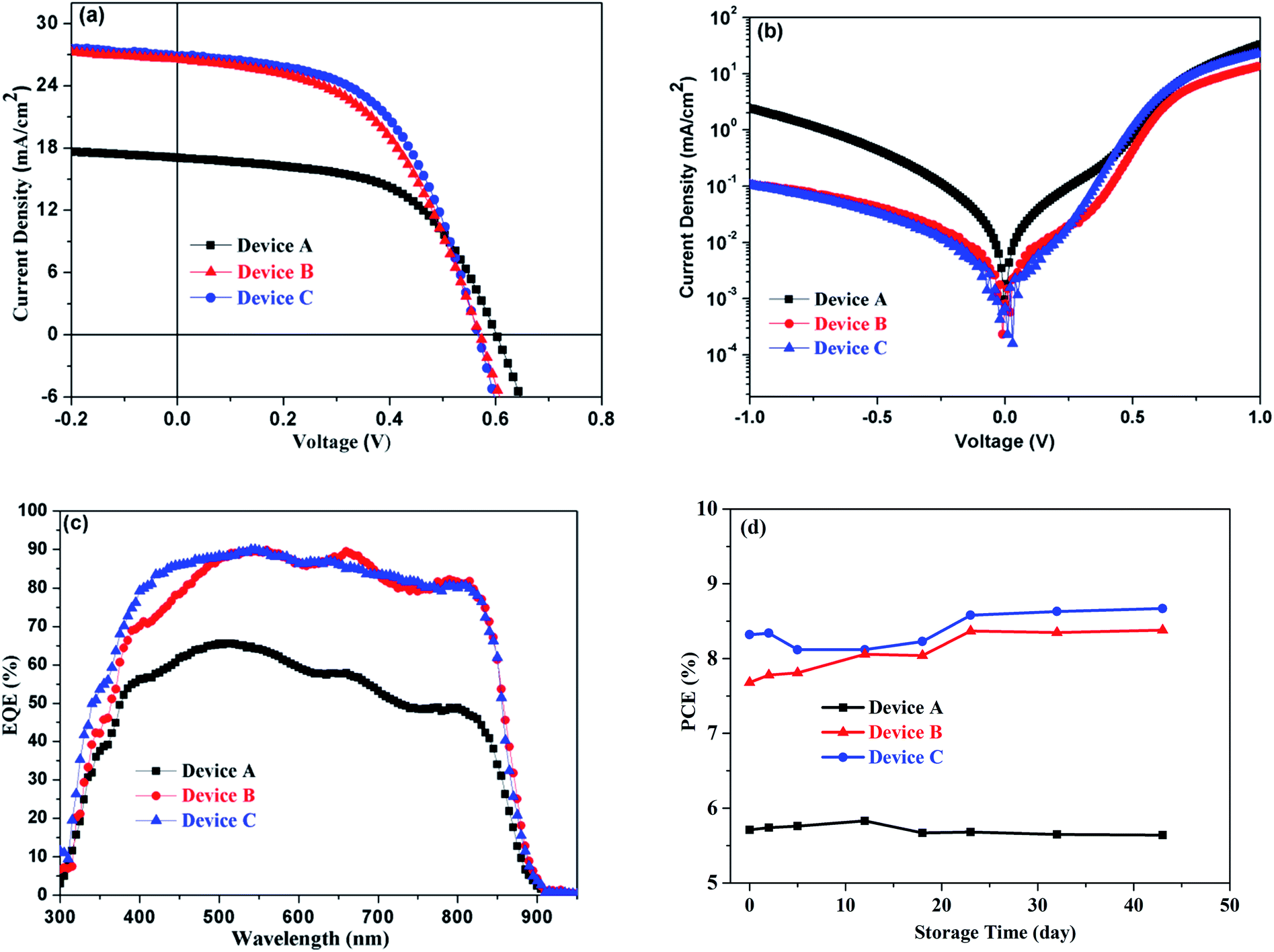 | ||
| Fig. 4 (a) J–V curves of CdTe NC devices w/o AVE under AM 1.5G (100 mW cm−2) illumination. Corresponding (b) dark J–V curves and (c) EQE spectra. (d) Stability of CdTe NC devices w/o AVE in ambient air. | ||
| Device name | PCE (%) | J SC (mA cm−2) | FF (%) | V OC (V) | R s (Ω cm2) | R sh (Ω cm2) |
|---|---|---|---|---|---|---|
| Device A | 5.83 | 17.06 | 56 | 0.61 | 9.1 | 283.9 |
| Device B | 8.34 | 27.66 | 51.1 | 0.59 | 6.5 | 349.6 |
| Device C | 8.67 | 27.33 | 54.7 | 0.58 | 6.4 | 334.1 |
The EQE spectra shown in Fig. 4c provide insights for understanding the JSC improvement for Device B and C. In comparison to that of Device A, the EQE of Device B or C shows significant improvement in the wavelength range from 400 to 850 nm, suggesting enhanced carrier collection with the help of AVE treatment since CdO or other impurities can be removed and interface defects can be decreased. In the end, a low carrier recombination is obtained at the back contact after AVE treatment. Therefore, a high JSC is expected in this case. It is well known that one of the key problems encountered in solution-processed CdTe NC solar cells is the device lifetime, which is greatly influenced by element migration such as Na, In and Sn into CdTe, and trap states originating from the oxidation of CdTe or CdSe. It is found that the stability of CdTe devices with AVE is very good (Fig. 4d). Detailed data about JSC, VOC and FF are shown in Fig. S6.† The device efficiency is not decreased but increased after 40 days, which may be due to the diffusion of Se into the CdTe layer or Te into the CdSe layer, leading to decreased bulk defects and formation of homogeneous CdSexTe1−x alloys.34,35
To gain more insights into the reason for device performance improvement, the charge recombination dynamics is investigated by tracking the transient voltage change in the charge population, as shown in Fig. 5a. The charge recombination time for Device A and Device B is 1.26 μs and 1.93 μs, respectively, implying that the charge recombination rate is low for Device B due to the long carrier lifetime. Furthermore, electrochemical impedance spectra (EIS) are used to study the electrical parameters in CdTe NC solar cells w/o AVE (device structure: ITO/ZnO/CdSe/CdTe (w/o AVE)/Au) at 0 V in the dark. Fig. 5b presents the semicircular Nyquist plot, in which an equivalent circuit is defined according to the device structure. R0 corresponds to the electrode resistance including ITO/ZnO and Au; R1 and C1 correspond to the CdSe/CdTe junction; R2 and C2 correspond to the two electrical contacts between ZnO/CdSe and CdTe/Au. Device B with AVE treatment shows a larger R2 value than Device A without AVE treatment, which is related to the weaker carrier recombination in the AVE-treated CdTe/Au contacts.36,37 Therefore, significant enhancements of JSC and PCE are achieved. To ascertain the charge transport properties of CdTe NC films w/o AVE, hole-only devices with an architecture of ITO/CdTe (100 nm)/Au (80 nm) are investigated. The space-charge-limited-current (SCLC) method is used to calculate the hole carrier mobility of CdTe NC thin films based on the equation  ,38 where ε0 is the permittivity of free space, εr = 9.8 is the relative dielectric constant of CdTe, L is the thickness of CdTe NCs, μp is the hole mobility, V is the applied voltage, and Vbi is the built-in voltage. As shown in Fig. 5c, the mobilities of devices with and without AVE are 1.15 × 10⁻³ cm2 V−1 s−1 and 8.56 × 10⁻⁴ cm2 V−1 s−1, respectively. Therefore, the higher mobility value of the film with AVE than of the film without AVE is attributed to the formation of a Te-rich surface on the AVE-processed CdTe NC film. Furthermore, the conductivity of the AVE-treated CdTe film (device structure: glass/CdTe (AVE treatment)/Au) is more than 20 times higher than that of the untreated CdTe film (Fig. S7†), indicating that a low-resistance Te rich surface is definitely formed after AVE treatment. Fig. 5d shows a schematic diagram of the energy band bending at the interface of CdTe/Au w/o AVE. It is noted that AVE treatment helps to form the p+ doped interface. The energy barrier for hole transfer from CdTe to Au is decreased and thus the carrier collection efficiency is improved in this case.
 | ||
| Fig. 5 (a) TPV curves of CdTe NC devices w/o AVE. (b) EIS of CdTe NC devices w/o AVE characterized at a bias of 0 V in the dark. The inset shows the equivalent electrical circuit diagram for analysis of charge dynamics. (c) SCLC fitting lines of hole-only devices (device structure: ITO/CdTe (100 nm) (w/o AVE)/Au). (d) Energy level alignment between CdTe and Au w/o AVE treatment. | ||
Conclusions
In conclusion, for the first time we have developed a new and robust method of AVE for inverted solution-processed CdTe NC solar cells. By controlling the vapor etching conditions, a p+-type Te-rich layer is generated, which is advantageous to decreasing the contact resistance and reducing interface recombination. Devices with NA and BM etching deliver high PCEs of 8.38% and 8.67%, respectively, which are among the highest PCEs ever reported for solution-processed CdTe NC based solar cells with an inverted structure. The excellent device performance with the use of the AVE method mainly comes from the low recombination loss at the interface of the CdTe/Au back electrode, which is verified by a series of electrical and optical measurements. Moreover, the device with AVE treatment shows very good operational stability with no decay when measured under ambient conditions. This work illustrates that the simple AVE approach can be applied to the future manufacture of low-cost solution-processed CdTe NC solar cells.Author contributions
X. G. and D. Q. conceived and designed the experiments; Z. R. and K. Y. synthesized the materials; X. G fabricated the solar cells; L. W., B. C. and Z. L. characterized the solar cells; H. W., Y. M. and L. H. contributed analysis tools; X. G. and S. L. analyzed the data; D. Q., L. H., X. G., Z. R. and L. H. wrote the paper. Authorship must be limited to those who have contributed substantially to the work reported.Conflicts of interest
There are no conflicts to declare.Acknowledgements
We acknowledge the financial support of the National Natural Science Foundation of China (No. 21875075, 61774077, 61274062, and 61775061), Guangdong Province Natural Science Fund (No. 2018A0303130041), Guangzhou Science and Technology Plan Project (No. 201804010295), National Undergraduate Innovative and Entrepreneurial Training Program (No. 201810561013) and Fundamental Research Funds for the Central Universities.References
- J. Jasieniak, B. I. MacDonald, S. E. Watkins and P. Mulvaney, Nano Lett., 2011, 11, 2856 CrossRef CAS PubMed.
- J. D. Major, R. E. Treharne, L. J. Phillips and K. Durose, Nature, 2014, 511, 334 CrossRef CAS PubMed.
- L. Kranz, C. Gretener, J. Perrenoud, D. Jaeger, S. S. A. Gerstl, R. Schmitt, S. Buecheler and A. N. Tiwari, Adv. Energy Mater., 2014, 4, 1301400 CrossRef.
- T.-C. Hou, Y. Yang, Z.-H. Lin, Y. Ding, C. Park, K. C. Pradel, L.-J. Chen and Z. L. Wang, Nano Energy, 2013, 2, 387 CrossRef CAS.
- J. M. Kurley, M. G. Panthani, R. W. Crisp, S. U. Nanayakkara, G. F. Pach, M. O. Reese, M. H. Hudson, D. S. Dolzhnikov, V. Tanygin, J. M. Luther and D. V. Talapin, ACS Energy Lett., 2017, 2, 270 CrossRef CAS.
- H. Lin, W. Xia, H. N. Wu and C. W. Tang, Appl. Phys. Lett., 2010, 97, 69 Search PubMed.
- T. K. Townsend and E. E. Foos, Phys. Chem. Chem. Phys., 2014, 16, 16458 RSC.
- W. Yoon, T. K. Townsend, M. P. Lumb, J. G. Tischler and E. E. Foos, IEEE Trans. Nanotechnol., 2014, 13, 551 CAS.
- T. Schmidt, K. Durose, C. Rothenhäusler and M. Lerch, Thin Solid Films, 2000, 361, 383 CrossRef.
- C. A. Wolden, A. Abbas, J. Li, D. R. Diercks, D. M. Meysing, T. R. Ohno, J. D. Beach, T. M. Barnes and J. M. Walls, Sol. Energy Mater. Sol. Cells, 2016, 147, 203 CrossRef CAS.
- D. Xiao, X. Li, D. Wang, Q. Li, K. Shen and D. Wang, Sol. Energy Mater. Sol. Cells, 2017, 169, 61 CrossRef.
- N. R. Paudel, C. Xiao and Y. Yan, Prog. Photovoltaics, 2015, 23, 437 CAS.
- D. Grecu, A. D. Compaan, D. Young, U. Jayamaha and D. H. Rose, J. Appl. Phys., 2000, 88, 2490 CrossRef CAS.
- A. Romeo, M. Terheggen, D. Abou-Ras, D. L. Bätzner, F. -J. Haug, M. Kälin, D. Rudmann and A. N. Tiwari, Prog. Photovoltaics, 2004, 12, 93 CAS.
- T. D. Dzhafarov, S. S. Yesilkaya, N. Y. Canli and M. Caliskan, Sol. Energy Mater. Sol. Cells, 2005, 85, 371 CrossRef CAS.
- K. D. Dobson, I. V. Fisher, G. Hodes and D. Cahen, Sol. Energy Mater. Sol. Cells, 2000, 62, 295 CrossRef CAS.
- I. M. Dharmadasa, J. M. Thornton and R. H. Williams, Appl. Phys. Lett., 1989, 54, 137 CrossRef CAS.
- O. V. Galán, A. C. Orea, C. M. García, J. Fandiño and M. F. G. Sánchez, Thin Solid Films, 2011, 519, 7164 CrossRef.
- V. Y. Novikov, Scr. Mater., 1998, 39, 945 CrossRef CAS.
- Q. Zeng, L. Hu, J. Cui, T. Feng, X. Du, G. Jin, F. Liu, T. Ji, F. Li, H. Zhang and B. Yang, ACS Appl. Mater. Interfaces, 2017, 9, 31345 CrossRef CAS PubMed.
- X. Du, Z. Chen, F. Liu, Q. Zeng, G. Jin, F. Li, D. Yao and B. Yang, ACS Appl. Mater. Interfaces, 2016, 8, 900 CrossRef CAS PubMed.
- S. Wen, M. Li, J. Yang, X. Mei, B. Wu, X. Liu, J. Heng, D. Qin, L. Hou, W. Xu and D. Wang, Nanomaterials, 2017, 7, 380 CrossRef PubMed.
- X. Guo, Q. Tan, S. Liu, D. Qin, Y. Mo, L. Hou, A. Liu, H. Wu and Y. Ma, Nano Energy, 2018, 46, 150 CrossRef CAS.
- M. G. Panthani, J. M. Kurley, R. W. Crisp, T. C. Dietz, T. Ezzyat, J. M. Luther and D. V. Talapin, Nano Lett., 2014, 14, 670 CrossRef CAS PubMed.
- Y. Tian, Y. Zhang, Y. Lin, K. Gao, Y. Zhang, K. Liu, Q. Yang, X. Zhou, D. Qin, H. Wu, Y. Xia, L. Hou, L. Lan, J. Chen, D. Wang and R. Yao, J. Nanopart. Res., 2013, 15, 1 Search PubMed.
- H. Liu, Y. Tian, Y. Zhang, K. Gao, K. Lu, R. Wu, D. Qin, H. Wu, Z. Peng, L. Hou and W. Huang, J. Mater. Chem. C, 2015, 3, 4227 RSC.
- Y. Xie, Q. Tan, Z. Zhang, K. Lu, M. Li, W. Xu, D. Qin, Y. Zhang, L. Hou and H. Wu, J. Mater. Chem. C, 2016, 4, 6483 RSC.
- S. Liu, W. Liu, J. Heng, W. Zhou, Y. Chen, S. Wen, D. Qin, L. Hou, D. Wang and H. Xu, Coatings, 2018, 8, 26 CrossRef.
- Z. C. Feng, H. C. Chou and A. Rohatgi, J. Appl. Phys., 1996, 79, 2151 CrossRef CAS.
- F. G. Fard, T. Hashemi, K. J. D. Mackenzie and C. A. Hogarth, J. Mater. Sci., 1983, 18, 3679 CrossRef.
- W. J. Danaher, L. E. Lyons, M. Marychurch and G. C. Morris, Appl. Surf. Sci., 1986, 27, 338 CrossRef.
- I. M. Kotina, L. M. Tukhkonen, G. V. Patsekina, A. V. Shchukarev and G. M. Gusinskii, Semicond. Sci. Technol., 1998, 13, 890 CrossRef CAS.
- M. A. Green, Y. Hishikawa, E. D. Dunlop, D. H. Levi, J. H. Ebinger and A. W. Y. Ho-Baillie, Prog. Photovoltaics, 2018, 26, 427 Search PubMed.
- J. D. Poplawsky, W. Guo, N. Paudel, A. Ng, K. More, D. Leonard and Y. Yan, Nat. Commun., 2016, 7, 12537 CrossRef CAS PubMed.
- B. I. MacDonald, A. Martucci, S. Rubanov, S. E. Watkins, P. Mulvaney and J. J. Jasieniak, ACS Nano, 2012, 6, 5995 CrossRef CAS PubMed.
- J. Tang and E. H. Sargent, Adv. Mater., 2011, 23, 12 CrossRef CAS PubMed.
- C.-E. Cheng, Z. Pei, C.-C. Hsu, C.-S. Chang and F. S.-S. Chien, Sol. Energy Mater. Sol. Cells, 2014, 121, 80 CrossRef CAS.
- J. Zhu, Y. Yang, Y. Gao, D. Qin, H. Wu, L. Hou and W. Huang, Nanotechnology, 2014, 25, 365203 CrossRef PubMed.
Footnotes |
| † Electronic supplementary information (ESI) available. See DOI: 10.1039/c9se00902g |
| ‡ These authors contributed equally to this work. |
| This journal is © The Royal Society of Chemistry 2020 |