
Application of a Sn4+ doped In2S3 thin film in a CIGS solar cell as a buffer layer†
SeongYeon
Kim
a,
Md. Salahuddin
Mina
a,
Kiwhan
Kim
b,
Jihye
Gwak
b and
JunHo
Kim
 *a
*a
aDepartment of Physics, Incheon National University, Incheon 22012, Republic of Korea. E-mail: jhk@inu.ac.kr
bPhotovoltaics Laboratory, Korea Institute of Energy Research (KIER), Daejeon 34129, Republic of Korea
First published on 24th October 2019
Abstract
As a Cd-free buffer, In2S3 buffer has been used in Cu(In,Ga)Se2 (CIGS) solar cells. To increase the carrier density of the In2S3 buffer, we doped Sn4+ into the buffer layer, which acted as an electron dopant in the In2S3 buffer layer. It was found that an optimal Sn4+ doping into the In2S3 buffer enhanced the power conversion efficiency of the CIGS solar cell. The deep defect states were reduced at both the bulk and surface of the CIGS solar cell by Sn4+ doping. The capacitance–voltage (C–V) charge density profile showed an increased depletion width in CIGS with the Sn4+ doped In2S3 buffer, thus implying an increase in the electron charge density in the Sn4+ doped In2S3 buffer. At 3% Sn4+ doping into the In2S3 buffer, the power conversion efficiency (PCE) was increased from 10.05% (CIGS solar cell with non-doped In2S3 buffer) to 14.52%.
1. Introduction
The chalcopyrite Cu (In,Ga)Se2 (CIGS) solar cell has been investigated for a long time and has been continuously developed to achieve a high power conversion efficiency (PCE). Recently, a solar frontier achieved a champion cell efficiency of 23.35%, which attracted much attention because of its high efficiency and good stability.1 The CIGS solar cell usually adopts a CdS thin film as a buffer. Cd diffuses into the CIGS absorber and easily forms a buried pn junction to produce a high efficiency CIGS solar cell with high reproducibility.2,3 However, Cd is toxic to the human body and environment, and the chemical solution-based process for CdS coating generates a waste-management problem. It was also noted that the champion cell with 23.35% efficiency used a Zn(O,S) buffer, not a CdS buffer. For the implementation of the CIGS solar cell in an ordinary life-like partial power source for building integrated photovoltaics (BIPV), IT devices, transports, etc., a Cd-free buffer is desirable.To avoid Cd, solar cells with a Cd-free buffer, Cd-reduced buffer, and buffer-free layer were developed. For environment-friendly solar cells with an alternative buffer layer, several Cd-free buffer layers such as Zn(O,S),4,5 (Zn,Mg)O,6,7 (Zn,Sn)O8 and In2S3 (ref. 9–13) were developed, and those Cd-free buffers showed a higher efficiency that was more than 17–18%. Oxide-based buffers usually have a wide band gap that is more than ∼3 eV, which allows CIGS to absorb more blue photons and resultantly increases the short circuit current (Jsc) by generating more photocurrents in the blue photon range. In order to reduce Cd, the deposition of a Cd-free buffer on a Cd-treated CIGS absorber14,15 and slightly Cd-treated CIGS16 were investigated. In the Cd-reduced buffer, Cd was used just for the surface treatment of the CIGS surface, which created a buried pn junction in CIGS and protected it from possible plasma damage during the sputtering of the Zn(O,S) buffer.15 The reduced CdS also passed more blue photons to the CIGS absorber, generating more currents in the blue photon spectrum range. For the Cd-free buffer, Al-doped Zn(O,S) was proposed to deposit directly on the CIGS absorber.17 The conduction band of TCO (Al: Zn(O,S)) was shifted upwards by S-alloying so that the shunt resistance was substantially increased to make a high efficiency cell without a buffer.
Among the Cd-free buffers, the In2S3 buffer was investigated relatively less. In2S3 can be fabricated by various methods such as thermal evaporation,10 ILGAR,11 ALD,12 and spray pyrolysis.13 Spray deposition has several advantages. It is low in cost, easy to scale up for the large area deposition of both rigid and flexible substrates, and it can be performed under air ambient conditions. In addition, spray deposition easily makes doped films by preparing the precursor solution with the doped element in a designed concentration. In2S3 buffer has also been applied to CZTS solar cells. Kim et al. applied In2S3/CdS double buffer to a CZTS solar cell and achieved a PCE of 12.4% with a high open circuit voltage (Voc), which was very close to that of the CZTS champion cell efficiency (12.6%).18 According to them, when In was used as an additional buffer over CdS, In could be substituted into the Cd site. Then, the generated InCd could be a dopant to the CdS layer since the oxidation state of In is In3+ and that of Cd is Cd2+. When In was further diffused into the CZTS absorber, it could be substituted into the Sn site, which acted as an acceptor since the Sn ion in CZTS is Sn4+. If the carrier concentration of the buffer and absorber was increased, the open circuit voltage increased. Kim et al. claimed that the Voc and PCE were increased after using the In2S3/CdS double buffer for the CZTS solar cell. Inspired by their experiment, we tried to perform donor doping into the In2S3 buffer layer by Sn4+. In the periodic table, Sn is located just to the right of In and Sn can be easily substituted in the In site. We fabricated a Sn4+ doped In2S3 buffer by spray pyrolysis, where Sn4+ served as the dopant in the In2S3 buffer, thus increasing the electron density in the In2S3 buffer. We found that the PCE increased in the solar cell with the Sn4+ doped In2S3 buffer compared to the pure In2S3 buffer. In order to understand the PCE improvement, we performed a comparison study of solar cells with undoped In2S3 buffer and Sn4+ doped In2S3 buffer. We reported the factors contributing to the PCE improvement of the CIGS solar cell with Sn4+ doped In2S3.
2. Experimental details
2.1. Fabrication of Sn4+ or Sn2+ doped In2S3 buffers
We deposited all of the In2S3-based buffers by the spray pyrolysis method. For the preparation of the Sn4+ or Sn2+ doped In2S3 solution, a dilution technique process was applied. First, we prepared 45 mL of a deionized aqueous solution, where InCl3 and SC(NH2)2 were dissolved with a molar ratio of InCl3![[thin space (1/6-em)]](https://www.rsc.org/images/entities/char_2009.gif) :SC(NH2)2 = 1:12 (0.1106 g:0.4567 g), which was equal to a 10 mM concentration for a 50 mL aqueous solution. Second, to create Sn stock solutions as dopants, we also prepared another 100 mL of a DI-water solution with 10 mM concentration of SnCl2·2H2O (for Sn2+ doping) or SnCl4·5H2O (for Sn4+ doping). Then, a small amount of the Sn stock solution was obtained with a syringe and mixed with some amount of the solution dissolved with InCl3 and SC(NH2)2 according to the Sn doping concentration. Using this process, we prepared precursor solutions with Sn concentrations of 0, 1, 2, 3, and 5%. Pure In2S3 was equal to 0% Sn4+ doped In2S3. Herein, we prepared the Sn2+ doped In2S3 solution, deposited the Sn2+ doped In2S3 thin film, and fabricated solar cells with the Sn2+ doped In2S3 buffers for a comparison study with a Sn4+ doped In2S3 thin film, which could provide ESI† to understand the effect of Sn4+ doping.
:SC(NH2)2 = 1:12 (0.1106 g:0.4567 g), which was equal to a 10 mM concentration for a 50 mL aqueous solution. Second, to create Sn stock solutions as dopants, we also prepared another 100 mL of a DI-water solution with 10 mM concentration of SnCl2·2H2O (for Sn2+ doping) or SnCl4·5H2O (for Sn4+ doping). Then, a small amount of the Sn stock solution was obtained with a syringe and mixed with some amount of the solution dissolved with InCl3 and SC(NH2)2 according to the Sn doping concentration. Using this process, we prepared precursor solutions with Sn concentrations of 0, 1, 2, 3, and 5%. Pure In2S3 was equal to 0% Sn4+ doped In2S3. Herein, we prepared the Sn2+ doped In2S3 solution, deposited the Sn2+ doped In2S3 thin film, and fabricated solar cells with the Sn2+ doped In2S3 buffers for a comparison study with a Sn4+ doped In2S3 thin film, which could provide ESI† to understand the effect of Sn4+ doping.
With the prepared solution, we sprayed the pure In2S3 buffer and Sn4+ doped In2S3 buffers on the CIGS absorbers, which were fabricated at the Korea Institute of Energy Research (KIER) with a three-stage thermal co-evaporation process. The spray deposition was performed for 10 minutes at a substrate temperature of 390 °C. The setting temperature of the hot plate was 390 °C. The deposited In2S3 buffer was measured to be ∼130 nm.
For comparison with the In2S3-based buffer, we also coated CdS by chemical bath deposition (CBD). The CBD process for the CdS buffer is well known and reported elsewhere.19–23
2.2. Fabrication of CIGS solar cell
After the buffer layer deposition on the CIGS samples, we subsequently deposited ∼60 nm of i-ZnO and ∼360 nm of the ITO layers by a RF-magnetron sputtering process to fabricate the solar cells. During the deposition of both films, the substrate was heated at 160 °C. For the deposition of i-ZnO, we set the working pressure at 7 mTorr with only Ar gas and applied a 40 W RF to the ZnO target. For the deposition of ITO, the working pressure was set at about 5 mTorr with Ar and O2 gas with a Ar/O2 ratio of 35 sccm/1 sccm. A RF power of 120 W was applied.2.3. Characterization of thin films and CIGS solar cells
We investigated the film morphology and chemical composition of the thin film using field emission scanning electron microscopy (FE-SEM) (JSM-7001F, Jeol) equipped with energy-dispersive X-ray spectroscopy (EDS) (INCA, Oxford). The optical transmission of the In2S3-based buffer was performed using a UV-visible spectrometer (Lambda 40, PerkinElmer). We examined the binding energy of the doped Sn ions in the In2S3 buffer using X-ray photoemission spectroscopy (PHI 5000 Versaprobe-II, ULVAC-PHI). To study the optical properties of the CIGS absorber, we measured the photoluminescence (PL) and time-resolved photoluminescence (TRPL) at room temperature by a minority lifetime measurement system (C12132, Hamamatsu). For these measurements, a laser excitation wavelength of 532 nm (pulse type) with 1.36 mW excitation power was used, which was set at a pulse repetition rate of 15 kHz and a duration time of 1 ns.The current density–voltage (J–V) under AM1.5G filtered illumination of a 1000 W m−2 Xe lamp (Abet Technology) was measured with a source meter (Keithley 2400). For the current density–voltage–temperature (J–V–T) measurement, we used a home-made cryostat, which could cool the stage to 90 K using liquid nitrogen.
Admittance spectroscopy (AS) and capacitance–voltage (C–V) measurements were performed with a LCR meter (E4980A, Agilent) to characterize the defect states of the CIGS absorber. For the AS measurement, an AC frequency was applied to the solar cell device from 20 Hz to 2 MHz at measurement temperatures of 300–90 K.
3. Results and discussion
Fig. 1 shows J–V curves for the CIGS solar cells with a CdS buffer, pure In2S3 buffer, and (1–5%) Sn4+ doped In2S3 buffer. The optical properties of the In2S3 and (1–5%) Sn4+ doped In2S3 buffer are shown in Fig. S1,† where the optical band gap increased with Sn4+ doping from ∼2.81 eV to ∼2.93 eV. For those solar cells, the device parameters are summarized in Table 1. The solar cell with a pure In2S3 buffer showed an efficiency of 10.05%, whereas the solar cell with a CdS buffer showed an efficiency of 10.64%. Comparing the FF of the CdS and In2S3 buffered solar cell, the In2S3 buffered cell showed 57.32% and the CdS buffered cell showed 56.40%. The lower FF of 56.40% of the CdS buffered cell was unusual. We suspected that the CBD for CdS was not optimized or that the surface of the CIGS absorber was very damaged due to air exposure for long time (at least more than one day) before the deposition of buffer layer. The best cell efficiency of 14.52% was obtained from the solar cell with a 3% Sn4+ doped In2S3 buffer. Compared to the other Sn4+ doped In2S3 buffered cells, the most improved parameter in the 3% Sn4+ doped In2S3 buffered cell was the FF, which was 73.86%. In the 3% Sn4+ doped In2S3 buffered cell, the shunt resistance was so enhanced that it generated a higher FF. This implied that in that solar cell, the pn interface was well formed to not allow any current leakage through the interface. Fig. S2† shows the cross-sectional FE-SEM images of the CIGS solar cells with pure In2S3 as well as 3% Sn4+ and 5% Sn4+ doped In2S3 buffers. However, from these FE-SEM images, we could not see any differences between the solar cells. However, Kim et al. reported that the morphology of Sn-doped In2S3 could be modified depending on the Sn doping concentration.24 They made a Sn-doped In2S3 film with various Sn concentrations using CBD. They reported that at an optimal Sn doping concentration, the morphology of the In2S3 buffer could be changed to show a uniform and compact surface as well as an improved texture PCE with the increased shunt resistance. This explanation could be applied to our In2S3 buffer.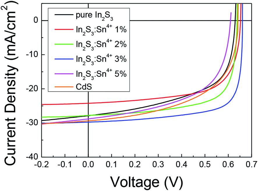 | ||
| Fig. 1 J–V curves of the CIGS solar cells with undoped and Sn4+ doped In2S3 buffers (0%, 1%, 2%, 3%, and 5%) as well as CdS buffer. | ||
| Items | Pure In2S3 | Sn4+ 1% | Sn4+ 2% | Sn4+ 3% | Sn4+ 5% | CdS |
|---|---|---|---|---|---|---|
| V oc (V) | 0.63 | 0.65 | 0.64 | 0.66 | 0.61 | 0.64 |
| J sc (mA cm−2) | 27.86 | 24.23 | 27.78 | 29.75 | 28.79 | 29.61 |
| Fill factor (%) | 57.32 | 66.54 | 69.60 | 73.86 | 56.36 | 56.40 |
| Efficiency (%) | 10.05 | 10.52 | 12.33 | 14.52 | 9.89 | 10.64 |
| R sh × A (ohm cm2) | 142.14 | 856.63 | 533.41 | 609.63 | 126.18 | 231.72 |
| R s × A (ohm cm2) | 1.95 | 2.17 | 1.48 | 1.37 | 2.45 | 2.48 |
| Area (cm2) | 0.12 | 0.12 | 0.13 | 0.14 | 0.13 | 0.10 |
We measured the J–V–T curves for the solar cells with pure In2S3 buffer and 3% Sn4+ doped In2S3 buffer to investigate the doping effect of Sn4+. Fig. 2 shows the J–V–T results and extracted Voc–T result. As the temperature was lowered, the Jsc decreased in the solar cell with pure In2S3 buffer. However, the Jsc was nearly constant at all temperatures in the solar cell with a 3% Sn4+ doped In2S3 buffer. The decrease in the Jsc with the lowering of temperature meant that deep level bulk defects were distributed in the CIGS absorber.23,25 As the temperature was lowered, the charge emission rate of the deep level decreased and it increased the trap (defect) assisted recombination, which induced a decrease in the Jsc at lower temperatures.23 Thus, with deeper defect levels at lower temperatures, the Jsc was further decreased. The negligible decrease in the Jsc in the solar cell with a 3% Sn4+ doped In2S3 buffer implied relatively shallower defects in the CIGS absorber. Since we used a CIGS absorber fabricated in the same batch, the quality difference between the CIGS absorbers was very small. However, before the fabrication of the CIGS solar cell, the CIGS absorber was exposed for a long time and the surface of the absorber was quite deteriorated. During the spray deposition of the In2S3 buffers at 390 °C, the deteriorated surface of the CIGS surface was cured. The excess S from the spray mist penetrated into the surface of the deteriorated surface of the CIGS absorber and passivated the defect states.26–28 The constant Jsc at all temperatures implied that the surface of CIGS with 3% Sn4+ doped In2S3 buffer was almost cured during the spray deposition. However, it is hard to explain why the 3% Sn4+ doped In2S3 cured the defects of the CIGS surface most effectively. From the Voc–T measurement, we extracted the activation energy (Ea). The Ea values for the pure In2S3 buffer and 3% Sn4+ doped In2S3 buffer were measured to be 1.16 eV and 1.21 eV, respectively. The smaller Ea meant the existence of a stronger interface recombination due to the interface defects.29 The Ea value of 1.21 eV indicated negligible interface defects in the pn junction of the solar cell with a 3% Sn4+ doped In2S3 buffer. This result also supported that the CIGS surface was well cured by the spray deposition of 3% Sn4+ doped In2S3 buffer. Fig. S3† shows the PL (a) and TRPL (b) results for all the fabricated solar cells. The PL intensity was very similar for the CIGS solar cells with an In2S3 buffer and 1–3% Sn4+ doped In2S3 buffers. However, the CIGS solar cell with the 5% Sn4+ doped In2S3 buffer showed a decreased PL intensity, indicating a degraded CIGS absorber. The minority carrier lifetime was measured to slightly increase from 6.19 ns for the pure In2S3 buffer to 6.45 ns for the 3% Sn4+ doped In2S3 buffer, whereas that for the 5% Sn4+ doped In2S3 buffer was estimated to be much reduced (4.89 ns). The longest lifetime for the 3% Sn4+ doped In2S3 buffer was consistent with the highest PCE of the solar cell with a 3% Sn4+ doped In2S3 buffer. The shortest lifetime of 4.89 ns for the 5% Sn4+ doped In2S3 buffer implied that the charge recombination centers that reduced the lifetime were formed in that CIGS absorber. Fig. S4† shows the EQE comparison of the CIGS solar cells with a In2S3 buffer and 3% Sn4+ doped In2S3 buffer, where the EQE value for the solar cell with a 3% Sn4+ doped In2S3 buffer was enhanced above ∼700 nm. This implied that the defect states in bulk CIGS were improved for the solar cell with a 3% Sn4+ doped In2S3 buffer.
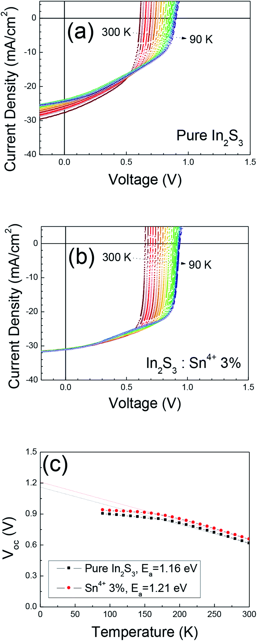 | ||
| Fig. 2 J–V–T results for the CIGS solar cells with a (a) pure In2S3 buffer and (b) 3% Sn4+ doped In2S3 buffer. (c) Voc–T results for both solar cells. | ||
Fig. 3 shows the AS results for the solar cells with a pure In2S3 buffer and 3% Sn4+ doped In2S3 buffer. The pure In2S3 buffered solar cell showed defect levels at 0.103 eV (Nt = 7.84 × 1014 cm−3) and 0.174 eV (Nt = 8.48 × 1014 cm−3), whereas the 3% Sn4+ doped In2S3 buffered solar cell showed shallower defect levels at 0.093 eV (Nt = 4.73 × 1014 cm−3) and 0.146 eV (Nt = 4.81 × 1014 cm−3). Herein, Nt is the integrated density for the corresponding peak. Fig. 3(b) and (d) show that the defect density (Nt) was also reduced in the cell with a 3% Sn4+ doped In2S3 buffer. The AS results were consistent with the J–V–T results in Fig. 2. The smaller Jsc decreased with lower temperatures for the CIGS cell with a pure In2S3, which was ascribed to the deeper defect levels with rather large defect densities in that absorber. This was confirmed by the AS results in Fig. 3.
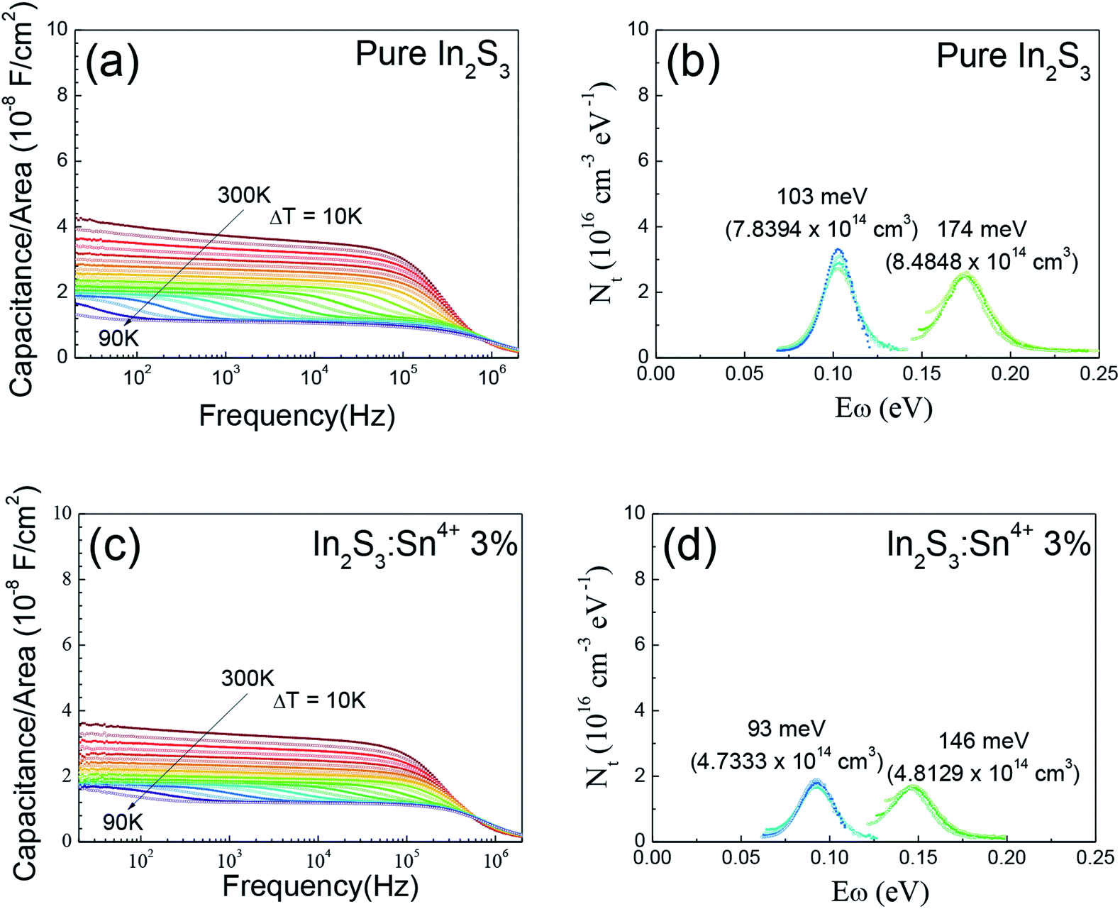 | ||
| Fig. 3 AS results for the CIGS solar cells with a (a) pure In2S3 buffer and (b) 3% Sn4+ doped In2S3 buffer. Defect density states for the solar cells with a (c) pure In2S3 buffer and (d) 3% Sn4+ doped In2S3 buffer. | ||
Fig. 4 shows the C–V charge density profiles for the In2S3 buffer and 3% Sn4+ doped In2S3 buffer. The two charge density profiles looked similar. However, near the CIGS absorber region, the charge density of CIGS with the 3% Sn4+ doped In2S3 buffer was slightly small. The depletion width shows a difference. The depletion width was measured to be 0.398 μm and 0.462 μm for the pure In2S3 buffer and 3% Sn4+ doped In2S3 buffer, respectively. Based on a textbook on semiconductor physics, the wider depletion width in the CIGS region meant that the carrier concentration for the n-type In2S3 counterpart was higher in the 3% Sn4+ doped In2S3 buffer. After doping Sn4+ into the In2S3 layer, the negative carrier concentration for the n-type In2S3 should have increased. The result in Fig. 4 implied an increase in the carrier concentration in the 3% Sn4+ doped In2S3 buffer.
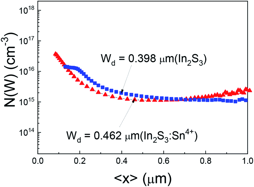 | ||
| Fig. 4 C–V charge density profiles of the CIGS solar cells with a pure In2S3 buffer and 3% Sn4+ doped In2S3 buffer. | ||
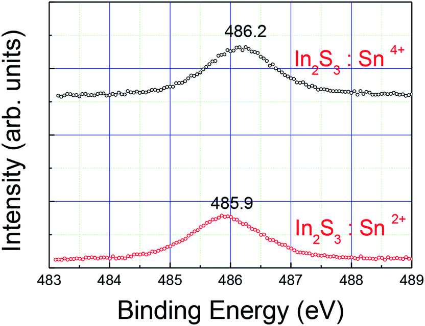
We checked the oxidation state of the Sn ion in the In2S3 buffer by XPS measurements. Fig. 5 shows the result of the XPS measurement. We prepared a 1% Sn2+ doped In2S3 buffer and 1% Sn4+ doped In2S3 film glass by spray pyrolysis. For the 1% Sn2+ doped sample, we dissolved SnCl2·2H2O into the spray solution of In2S3. The binding energy of the Sn 3d5/2 level was measured to be 485.9 eV and 486.2 eV for Sn2+ doped In2S3 and Sn4+ doped In2S3, respectively. In the XPS handbook, the binding energy of the Sn4+ oxidation state was larger than that of the Sn2+ oxidation state. The result in Fig. 5 shows that the Sn oxidation state of Sn used for the In2S3 buffers in the solar cells listed in Table 1 is Sn4+.
 | ||
| Fig. 5 Binding energy of the Sn 3d5/2 level for Sn4+ doped In2S3 and Sn2+ doped In2S3. | ||
We also made CIGS solar cells with a 1% Sn2+ doped In2S3 buffer and 3% Sn2+ doped In2S3 buffer. Fig. 6 shows the J–V results of the CIGS solar cells with Sn2+ doped In2S3 buffers. The results for the CIGS solar cells with a 1% Sn4+ doped buffer and 3% Sn4+ doped In2S3 buffer are also displayed again for comparison. The CIGS solar cells made with Sn2+ buffer showed very low cell efficiency. The solar cell with a 1% Sn2+ doped In2S3 buffer showed Voc = 0.63 V, Jsc = 11.41 mA cm−2, FF = 30.65%, and PCE = 2.21%. The solar cell with a 3% Sn2+ doped In2S3 buffer exhibited Voc = 0.66 V, Jsc = 17.69 mA cm−2, FF = 38.61%, and PCE = 4.52%. The Jsc and FF were much reduced in the CIGS solar cells with Sn2+ doped In2S3 buffers. We did not systematically investigate why the CIGS solar cell with a Sn2+ doped In2S3 buffer showed a lower efficiency. However, it was expected that Sn2+ doping into the In2S3 buffer reduced the electron carrier density, which increased the negative effects on the cell performance. Fig. S3† shows a minority carrier lifetime of ∼4.84 ns for a solar cell with a 1% Sn2+ doped In2S3 buffer, which was the shortest lifetime among the solar cells. This result implied that recombination centers were produced near the surface of the CIGS absorber by the deposition of the 1% Sn2+ doped In2S3 buffer. Fig. S4† shows the reduced EQE for the solar cell with a 1% Sn2+ doped In2S3 buffer, where the EQE was substantially reduced above ∼470 nm wavelength. This result also indicated that the surface and the area near the surface region of the CIGS absorber were degraded by the deposition of the 1% Sn2+ doped In2S3 buffer. From this result, we found that Sn2+ doping into the In2S3 buffer had a detrimental effect on the CIGS solar cell, whereas Sn4+ doping into the In2S3 buffer induced improvement in the PCE of the CIGS solar cell.
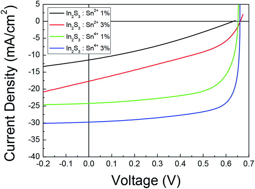 | ||
| Fig. 6 J–V results for the CIGS solar cells with the Sn2+ doped In2S3 buffer and Sn4+ doped In2S3 buffer. | ||
4. Conclusions
We fabricated CIGS solar cells with In2S3 buffer and Sn4+ doped In2S3 buffers. It was found that at an optimal doping (3%) of Sn4+, the PCE was enhanced to 14.52% from 10.05% for the CIGS solar cell with pure In2S3 buffer. The J–V–T and AS measurements revealed that the deep defect states at both the surface and bulk were substantially reduced in the CIGS solar cell with a 3% Sn4+ doped In2S3 buffer, which contributed to a PCE enhancement of 14.52%. The C–V charge density profiles indicated that the carrier concentration of the n-type buffer increased in the 3% Sn4+ doped In2S3 buffer compared to the pure In2S3 buffer. This result supported the increase in the electron density by Sn4+ doping into the In2S3 buffer. It was also confirmed that Sn2+ doping into the In2S3 buffer resulted in detrimental effects on the CIGS solar cell. The results reported in this paper proved that the PCE of the CIGS solar cell with a In2S3 buffer was improved by Sn4+ doping into the In2S3 buffer.Conflicts of interest
There are no conflicts to declare.Acknowledgements
This work was supported by the National Research Foundation of Korea (NRF). This work was funded by the Korean Government (NRF-2016M1A2A2937010 and 2017R1A2B2006223), the Korea Institute of Energy Technology Evaluation and Planning (KETEP), and the Ministry of Trade, Industry & Energy (MOTIE) of the Republic of Korea (No. 20173010012980 and No. 20183020010970).References
- M. A. Green, E. D. Dunlop, D. H. Levi, J. Hohl-Ebinger, M. Yoshita and A. W. Y. Ho-Baillie, Prog. Photovolt. Res. Appl., 2019, 27, 565–575 CrossRef.
- T. Nakada and A. Kunioka, Appl. Phys. Lett., 1999, 74, 2444–2446 CrossRef CAS.
- C.-S. Jiang, F. S. Hasoon, H. R. Moutinho, H. A. Al-Thani, M. J. Romero and M. M. Al-Jassim, Appl. Phys. Lett., 2003, 82, 127–129 CrossRef CAS.
- M. Nakamura, Y. Kouji, Y. Chiba, H. Hakuma, T. Kobayashi and T. Nakada, Proceedings of the 39th IEEE PVSC, Tampa, FL, USA, 2013, pp. 0849–0852 Search PubMed.
- M. Powalla, W. Witte, P. Jackson, S. Paetel, E. Lotter, R. Wuerz, F. Kessler, C. Tschamber, W. Hempel, D. Hariskos, R. Menner, P. Jackson, S. Paetel, W. Witte, W. Wischmann, M. Powalla, L. Burkert, T. Kolb, M. Oertel, B. Dimmler and B. Fuchs, Prog. Photovolt. Res. Appl., 2012, 20, 534–542 CrossRef.
- A. Hultqvist, C. Platzer-Bjorkman, T. Torndahl, M. Ruth and M. Edoff, Proceedings of the 22nd European Photovoltaic Solar Energy Conference, Milan, Italy, 2007, pp. 2381–2384 Search PubMed.
- T. Negami, T. Aoyagi, T. Satoh, S. Shimakawa, S. Hayashi and Y. Hashimoto, Proceedings of the 29th IEEE Photovoltaic Specialists Conference, New Orleans, LA, USA, 2002, pp. 656–659 Search PubMed.
- J. Lindahl, U. Zimmermann, P. Szaniawski, T. Torndahl, A. Hultqvist, P. Salome, C. Platzer-Bjorkman and M. Edoff, IEEE Journal of Photovoltaics, 2013, 3, 1100–1105 Search PubMed.
- M. Powalla, W. Witte, P. Jackson, S. Paetel, E. Lotter, R. Wuerz, F. Kessler, C. Tschamber, W. Hempel, D. Hariskos, R. Menner, A. Bauer, S. Spiering, E. Ahlswede, T. M. Friedlmeier, D. Blazquez-Sanchez, I. Klugius and W. Wischmann, IEEE Journal of Photovoltaics, 2014, 4, 440–446 Search PubMed.
- S. Kim, T. R. Rana and J. Kim, J. Korean Phys. Soc., 2017, 71, 1012–1018 CrossRef CAS.
- R. Saez-Araoz, J. Krammer, S. Harndt, T. Koehler, M. Krueger, P. Pistor, A. Jasenek, F. Hergert, M. C. Lux-Steiner and C.-H. Fischer, Prog. Photovolt. Res. Appl., 2012, 20, 855–861 CrossRef CAS.
- N. Naghavi, S. Spiering, M. Powalla, B. Canava and D. Lincot, Prog. Photovolt. Res. Appl., 2003, 11, 437–443 CrossRef CAS.
- D. B. Khadka, S. Kim and J. Kim, J. Phys. Chem. C, 2015, 119, 12226–12235 CrossRef CAS.
- D. H. Shin, L. Larina, K. H. Yoon and B. T. Ahn, Curr. Appl. Phys., 2010, 10, 5142–5145 Search PubMed.
- T. R. Rana, S. Kim, J. Kim, K. Kim and J. H. Yun, Sustainable Energy Fuels, 2017, 9, 1981–1990 RSC.
- M. A. Contreras, M. J. Romero, B. To, F. Hasoon, R. Noufi, S. Ward and K. Ramanathan, Thin Solid Films, 2002, 403–404, 204–211 CrossRef CAS.
- T. Minemoto and J. Julayhi, Curr. Appl. Phys., 2013, 13, 103–106 CrossRef.
- J. Kim, H. Hiroi, T. K. Todorov, O. Gunawan, M. Kuwahara, T. Gokmen, D. Nair, M. Hopstaken, B. Shin, Y. S. Lee, W. Wang, H. Sugimoto and D. B. Mitzi, Adv. Mater., 2014, 26, 7427–7431 CrossRef CAS PubMed.
- W. Witte, S. Spiering and D. Hariskos, Vak. Forsch. Prax., 2014, 26, 23–27 CrossRef CAS.
- J. Kessler, K. O. Velthaus, M. Ruck, R. Laichinger, H. W. Schock, D. Lincot, R. Ortega and J. Vedel, 6th International Photovoltaic Solar Energy Conference, New Delhi, 1992, p. 1005 Search PubMed.
- L. Kronik, L. Burstein, M. Leibovitch, Y. Shapira, D. Gal, E. Moons, J. Beier, G. Hodes, D. Cahen, D. Hariskos, R. Klenk and H. W. Schock, Appl. Phys. Lett., 1995, 67, 1405–1407 CrossRef CAS.
- P. Jackson, R. Wuerz, D. Hariskos, E. Lotter, W. Witte and M. Powalla, Phys. Status Solidi RRL, 2016, 10, 583 CrossRef CAS.
- F. Pianezzi, P. Reinhard, A. Chiril, S. Nishiwaki, B. Bissig, S. Buecheler and A. N. Tiwari, J. Appl. Phys., 2013, 114, 1945081–1945088 CrossRef.
- J. H. Kim, D. Shin and B. T. Ahn, Curr. Appl. Phys., 2016, 16, 1040–1045 CrossRef.
- S. Kim, T. R. Rana, J. Kim, D.-H. Son, K.-J. Yang, J.-K. Kang and D.-H. Kim, Nano Energy, 2018, 45, 75–83 CrossRef CAS.
- T. Zhang, Y. X. Yang, D. A. Liu, S. C. Tse, W. R. Cao, Z. B. Feng, S. Chen and L. Qian, Energy Environ. Sci., 2016, 9, 3674–3681 RSC.
- T. Nakada, H. Ohbo, T. Watanabe, H. Nakazawa, M. Matsui and A. Kunioka, Sol. Energy Mater. Sol. Cells, 1997, 49, 285–290 CrossRef CAS.
- T. Kobayashi, H. Yamaguchi, Z. J. L. Kao, H. Sugimoto, T. Kato, H. Hakuma and T. Nakada, Prog. Photovolt. Res. Appl., 2015, 23(10), 1367–1374 CrossRef CAS.
- S. S. Hegedus and W. N. Shafarman, Prog. Photovoltaics, 2004, 12, 155–176 CAS.
Footnote |
| † Electronic supplementary information (ESI) available. See DOI: 10.1039/c9se00778d |
| This journal is © The Royal Society of Chemistry 2020 |