
 Open Access Article
 This Open Access Article is licensed under a Creative Commons Attribution-Non Commercial 3.0 Unported Licence
Spontaneous S–Si bonding of alkanethiols to Si(111)–H: towards Si–molecule–Si circuits†
Chandramalika R.
Peiris
 a,
Simone
Ciampi
a,
Essam M.
Dief
a,
Jinyang
Zhang
a,
Peter J.
Canfield
bc,
Anton P.
Le Brun
d,
Daniel S.
Kosov
*e,
Jeffrey R.
Reimers
*bf and
Nadim
Darwish
*a
a,
Simone
Ciampi
a,
Essam M.
Dief
a,
Jinyang
Zhang
a,
Peter J.
Canfield
bc,
Anton P.
Le Brun
d,
Daniel S.
Kosov
*e,
Jeffrey R.
Reimers
*bf and
Nadim
Darwish
*a
aSchool of Molecular and Life Sciences, Curtin Institute of Functional Molecules and Interfaces, Curtin University, Bentley, WA 6102, Australia. E-mail: nadim.darwish@curtin.edu.au
bInternational Centre for Quantum and Molecular Structures, School of Physics, Shanghai University, Shanghai 200444, China
cSchool of Chemistry, The University of Sydney, NSW 2006, Australia
dAustralian Centre for Neutron Scattering, Australian Nuclear Science and Technology Organization (ANSTO), Lucas Heights, NSW 2234, Australia
eCollege of Science and Engineering, James Cook University, Townsville, QLD 4811, Australia. E-mail: daniel.kosov@jcu.edu.au
fSchool of Mathematical and Physical Sciences, University of Technology Sydney, NSW 2007 Australia. E-mail: Jeffrey.Reimers@uts.edu.au
First published on 27th April 2020
Abstract
We report the synthesis of covalently linked self-assembled monolayers (SAMs) on silicon surfaces, using mild conditions, in a way that is compatible with silicon-electronics fabrication technologies. In molecular electronics, SAMs of functional molecules tethered to gold via sulfur linkages dominate, but these devices are not robust in design and not amenable to scalable manufacture. Whereas covalent bonding to silicon has long been recognized as an attractive alternative, only formation processes involving high temperature and/or pressure, strong chemicals, or irradiation are known. To make molecular devices on silicon under mild conditions with properties reminiscent of Au–S ones, we exploit the susceptibility of thiols to oxidation by dissolved O2, initiating free-radical polymerization mechanisms without causing oxidative damage to the surface. Without thiols present, dissolved O2 would normally oxidize the silicon and hence reaction conditions such as these have been strenuously avoided in the past. The surface coverage on Si(111)–H is measured to be very high, 75% of a full monolayer, with density-functional theory calculations used to profile spontaneous reaction mechanisms. The impact of the Si–S chemistry in single-molecule electronics is demonstrated using STM-junction approaches by forming Si–hexanedithiol–Si junctions. Si–S contacts result in single-molecule wires that are mechanically stable, with an average lifetime at room temperature of 2.7 s, which is five folds higher than that reported for conventional molecular junctions formed between gold electrodes. The enhanced “ON” lifetime of this single-molecule circuit enables previously inaccessible electrical measurements on single molecules.
1. Introduction
Self-assembled monolayers have captured the attention of the scientific community owing to their ease of formation and affinity to different types of substrates, with a vast range of established applications in nano fabrications, sensors, biotechnology and molecular electronics. Considering electronics applications, thiol and dithiol SAMs, particularly on Au, have attracted considerable interests1–8 owing to their ease of preparation from gas phase or from solution.9 Although widely used, thiols on Au suffer from major drawbacks, including the high mobility of the S–Au bonds and the availability of a wide range of possible thiol–gold bonding motifs at quite similar energies.10 S–Au bonds are dominated by dispersion forces11,12 and are hence relatively weak,13 poorly directional, and can accommodate a wide range of coordination numbers.14–16In the last few years, there has been increasing interest in expanding the use of SAMs in nanoelectronics from gold8 towards semiconducting platforms including GaAs17–19 and Si.20–25 It is anticipated that combining the electrical properties of semiconductors with the chemical diversity of organic molecules, a variety of technological development can be achieved. Silicon, in particular, provides an attractive choice as an electrode because atomically flat silicon substrates are commercially available, are widely used in microelectronics industry, and their electronic properties can be controlled via doping and chemical variation.7,10,26–29
SAMs built upon covalent bonds to silicon were first assembled30 in 1993, utilizing Si–C bonds formed through activated free-radical chemistry. In one almost-trivial application, SAMs could replace SiO2 as the insulating material in field-effect transistors and other devices, providing better structural and chemical control,27,31–33 leading even to biomedical applications.34 Devices in which the interface forms a critical component10 include: quantum-dot photonics,35 light harvesting and usage,36,37 photoluminescence,38 general electrochemical applications39 including sensing,40 polymer engineering,41 hydrophobicity,42 general electrochemical sensors,43 bioimaging, biosensing, and cancer treatment,44,45 as well as molecular-electronics applications.26,39,46–50 Mostly the strategies used for making covalent bonds to silicon51 have involved conditions considered harsh for silicon engineering, including: radical initiators,30,52,53 Lewis acids,54 Grignard reagents,29,55 electrografting,56 and microwave57 or UV-visible irradiation,58–60 with many processes also requiring significant heating. Hence notable absences in the developed applications involving silicon–molecule interfaces are those that would involve integration into standard silicon-device fabrication.
We focus on covalent links between silicon and sulfur as a means of achieving this goal (Fig. 1). Molecules tethered to silicon in this way were first synthesized using ultra-high vacuum technologies,61,62 followed by high-temperature solution chemistry21,63 and even high-temperature high-pressure processes in supercritical CO2,64 as well as UV65–67 and visible68 photochemical approaches. Well-formed layers have been produced that are resistive to chemicals that could be applied in subsequent stages of CMOS processing,21 with junction characteristics useful for molecular electronics.26,46,69 Nevertheless, synthetic conditions involving the use of radical initiators, catalysts, high temperature and/or high pressure, or irradiation, are harsh, with even exposure to radiation known to induce SAM damage.70 To date, there has been no technology developed, using Si–S or other types of covalent bonding, that could be readily applied to integrate molecular electronics into silicon engineering.
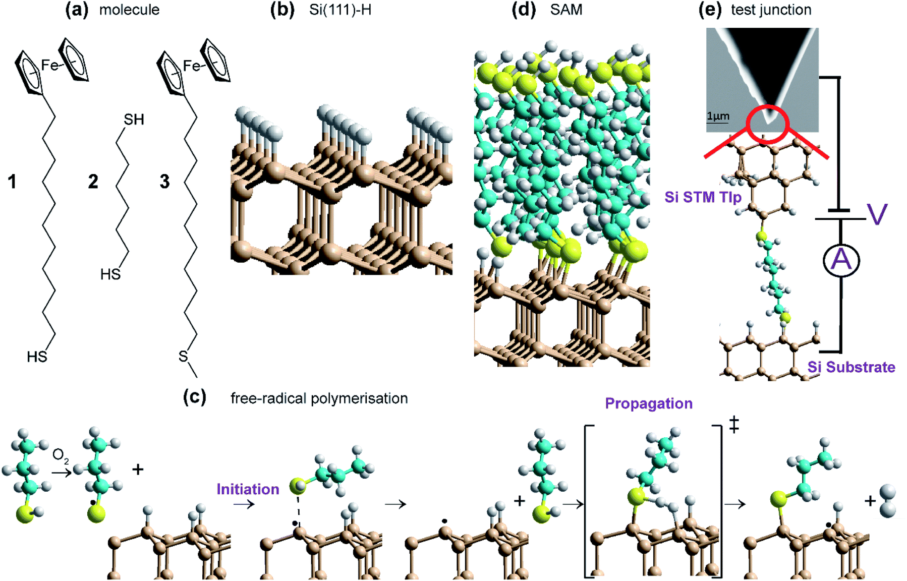 | ||
| Fig. 1 (a) Molecular and SAM structures: 1 enables electrochemical studies while 2 enables STM-junction studies and 3, without a thiol, is used as a control (a) molecules are reacted with H-terminated silicon surfaces (b) via a thiyl free-radical polymerization (c), as illustrated for propanethiol, to form covalently bonded SAMs (d). (e) Si–molecule–Si junction formed from 2 using single-molecule STM-junction technology (e). S – yellow, Si – fawn, C – cyan, H – white. | ||
Typically, organic interfaces to silicon are dominated by surface-layer silicon oxides,71 and hence device synthetic strategies often focus on conditions leading to oxide-free surfaces.10,27,29,32,34,55,64,72,73 Indeed, dangling bonds on the surface that survive SAM formation, and other functionalities, are susceptible to attack from O2, H2O, and other common ambient species, demanding that functional SAMs assemble at high coverage with low levels of flaws. The explicit exclusion of oxygen from reactions has therefore been a priority. Most reactions with silicon are believed to proceed via radial mechanisms,30,52,53,67,74–76 either through thermal or other production of surface radicals or else through the attack of radicals from solution on the surface. The presence of O2 in solutions of thiols spontaneously leads to radical production, without the need for harsh conditions such as high temperature, pressure, added chemical radical initiators, or applied radiation.
We demonstrate that indeed such reactions can form high-quality SAMs on Si(111), synthesizing highly stable, low-oxygen-content monolayers with electrical properties akin to classic SAMs incorporating Au–S interfaces. The reactions performed are sketched in Fig. 1 and involve reaction of two molecules 1 and 2 (Fig. 1a) with thiol groups (RSH) at least on one end, on H-terminated silicon (Fig. 1b); molecule 3, without a thiol, is used as a control. The products are identified as densely-packed Si–S-linked SAMs (Fig. 1d) based on extensive characterisation using X-ray reflectometry (XRR), atomic force microscopy (AFM), X-ray photoelectron spectroscopy (XPS) and cyclic voltammetry (CV) for determining SAM thickness, topography, surface composition and coverage. Reaction mechanisms (Fig. 1c) and SAM properties are then understood using density-functional theory (DFT) modelling of the reaction pathways, depicting a set of reactions leading to spontaneous SAM formation under ambient conditions through free-radical surface polymerization. Monolayers are formed using only mild conditions on Si containing different dopants (n- or p-type silicon), as well as on different crystal orientations (including (100) and (111)), indicating the versatility of the approach. Whilst 1 is used to form redox active monolayers, 2 containing thiol groups at both ends (Fig. 1a), is utilized in forming single-molecule circuits connected to two silicon electrodes in scanning-tunnelling microscopy (STM) break-junction (STM-BJ) experiments.
2. Results and discussion
2.1 Synthesis
SAMs of compound 1 and 2 was produced as described in Methods and summarized in Fig. 1. All operations in this method are universally available in silicon fabrication laboratories, with, in particular, the reaction of the thiol with the surface being as easy to perform as is standard gold–thiol chemistry. Critically, no heating, UV irradiation or external catalysis is required; note that performing the experiments under ultra-low light conditions did not affect outcome.The aspect of the synthesis of most note is the O2 content of the dichloromethane (DCM) solvent used in the reaction of the thiol and the prepared silicon surface. Using DCM as purchased and re-distilled, the reaction proceeds to completion on the 24 hour timescale. However, removal of O2 from the solvent resulted in SAMs of only ca. one tenth the coverage after the same period of time (see Fig. 2f). Hence the presence of dissolved O2 is critical to the reaction mechanism.
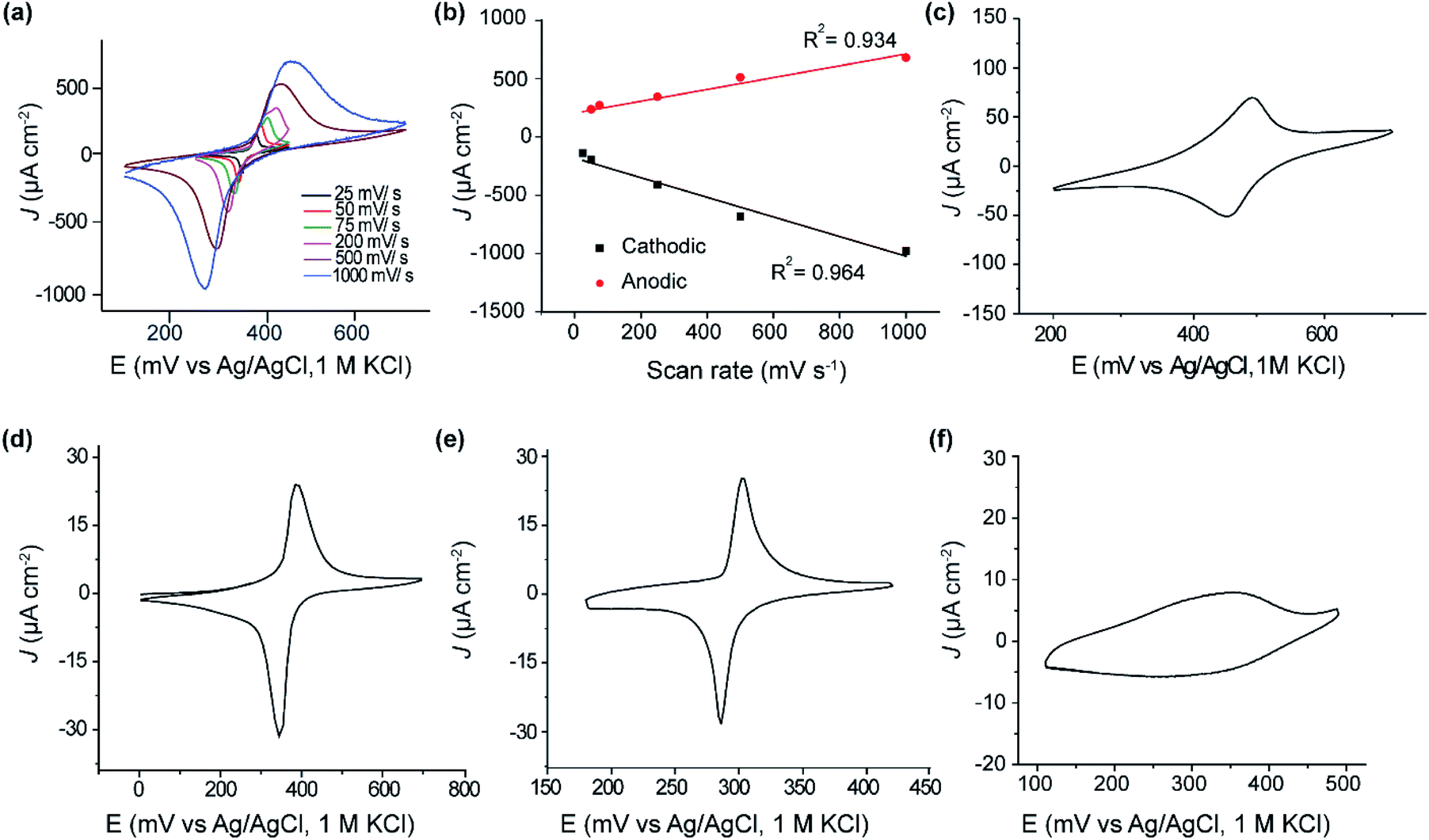 | ||
| Fig. 2 Cyclic voltammetry. (a) Cyclic voltammetry at different scan rates for a SAM of 1 on p-type Si(111)–H of resistivity 0.001 Ω cm. The estimated surface coverage is 2.53 × 10¹⁴ molecules cm−2. (b) Current versus scan rate for the SAM formed of 1. The current increases linearly with scan rate, indicating a surface redox reaction. (c) Cyclic voltammetry for a SAM of 1 on Si(111)–H at 50 mV s−1 on n-type phosphorus doped of resistivity 0.001 Ω cm. Coverage is dopant independent, the results leading to coverages of 2.50 × 10¹⁴ molecules cm−2 and is comparable to that obtained on p-type boron doped silicon shown in (a). (d) Cyclic voltammetry at 50 mV s−1 for SAMs of 1 on Au(111), showing very similar appearances to those reported for Si in (a) at a similar scan rate. The deduced coverages are 2.20 × 10¹⁴ molecules cm−2, slightly less than that for the corresponding monolayers on Si(111)–H. (e) Cyclic voltammetry at 50 mV s−1 for SAMs of 1 on Si(100)–H showing a similar appearances to those reported for Si(111)–H; however the surface coverage is lower and estimated at 9.3 × 10¹³ molecules cm−2. (f) Cyclic voltammetry for SAMs of 1 on Si(111)–H prepared from fresh solid of 1 dissolved in deoxygenated DCM. Oxygen was removed by bubbling Ar for 60 min in the DCM solution containing 1 using a septum sealed vessel and a needle as a vent. The SAM reaction flask was kept under a positive pressure of Ar during the 24 h reaction time. The surface coverage is estimated to be 2.10 × 10¹³ molecules cm−2 and is about 10% of that produced under ambient conditions. | ||
2.2 SAM characterization by cyclic voltammetry
Fig. 2a shows cyclic voltammograms obtained for SAM of 1 on p-type Si(111)–H. The estimated coverage of the ferrocenyl-terminated compound 1 is 2.53 × 10¹⁴ molecules cm−2, about the highest coverage possible for a layer of ferrocene molecules. This translates to 0.32 bound molecules for every surface silicon atom, suggesting a high-quality SAM at 1![[thin space (1/6-em)]](https://www.rsc.org/images/entities/char_2009.gif) :3 coverage, possibly on a (√3 × √3) supercell.
:3 coverage, possibly on a (√3 × √3) supercell.
Results shown in Fig. 2a, c and d indicate that this coverage is insensitive to doping (p-type or n-type) of the silicon. The shapes of the voltammetric waves and the surface coverage were comparable to a monolayer of the same molecule formed on Au(111) (Fig. 2d). The voltammetric waves were stable after extensive voltammetric cycling. Similar to thiol–gold monolayers, the peak current in thiol–silicon monolayers increase linearly with the scan rate, indicating a surface-bound electrochemical process (Fig. 2a and b).
Analogous results shown in Fig. 2e indicate that, independent of doping, the adsorbate coverage on Si(100) is 9.3 × 10¹³ molecules cm−2, one third of that observed on Si(111)–H. As a ratio of the number of surface Si atoms, this coverage is 1:7.3, a value difficult to understand based on the surface symmetry and adsorbate size which would suggest likely values of 1:2 or 1:4. The Si(100) surface used has not undergone its possible (2 × 1) reconstruction and hence two H atoms protrude from each surface Si atom, so only one in fifteen surface hydrogens were replaced. Hence, while the same chemical reaction is likely to be occurring independent of the silicon surface used, only Si(111)–H appears useful for the production of dense and regular SAMs, as is needed for large scale molecular electronics devices. It is possible that method modifications could yield higher coverages, however, as electronically functional alkane SAMs on Si(100), with a coverage of 3 ± 1 × 10¹⁴ molecules cm−2, have been produced using UV irradiation,66 with high coverages also produced utilizing thermal surface-radical production.77
2.3 SAM characterization by AFM and C-AFM
Fig. 3a and S1 in ESI† show 10 × 10 μm2 and 20 × 20 μm2 AFM images, respectively, of a p-type Si(111)–H surface covered by the dithiol 2. The topography shows flat terraces separated by atomic steps. The peak-to-peak roughness measured within one Si(111) terrace is ca. 1.7 Å, consistent with an atomically smooth alkyl monolayer on Si(111).78 Further, the high-quality topography confirms that the SAMs are homogeneous monolayers at the nanoscale, free of any contaminants or oxidative products or etched regions. These properties parallel those of SAMs produced by other means,21,64,65,68,74,75 despite the utilization of dissolved O2 in the reaction mechanism.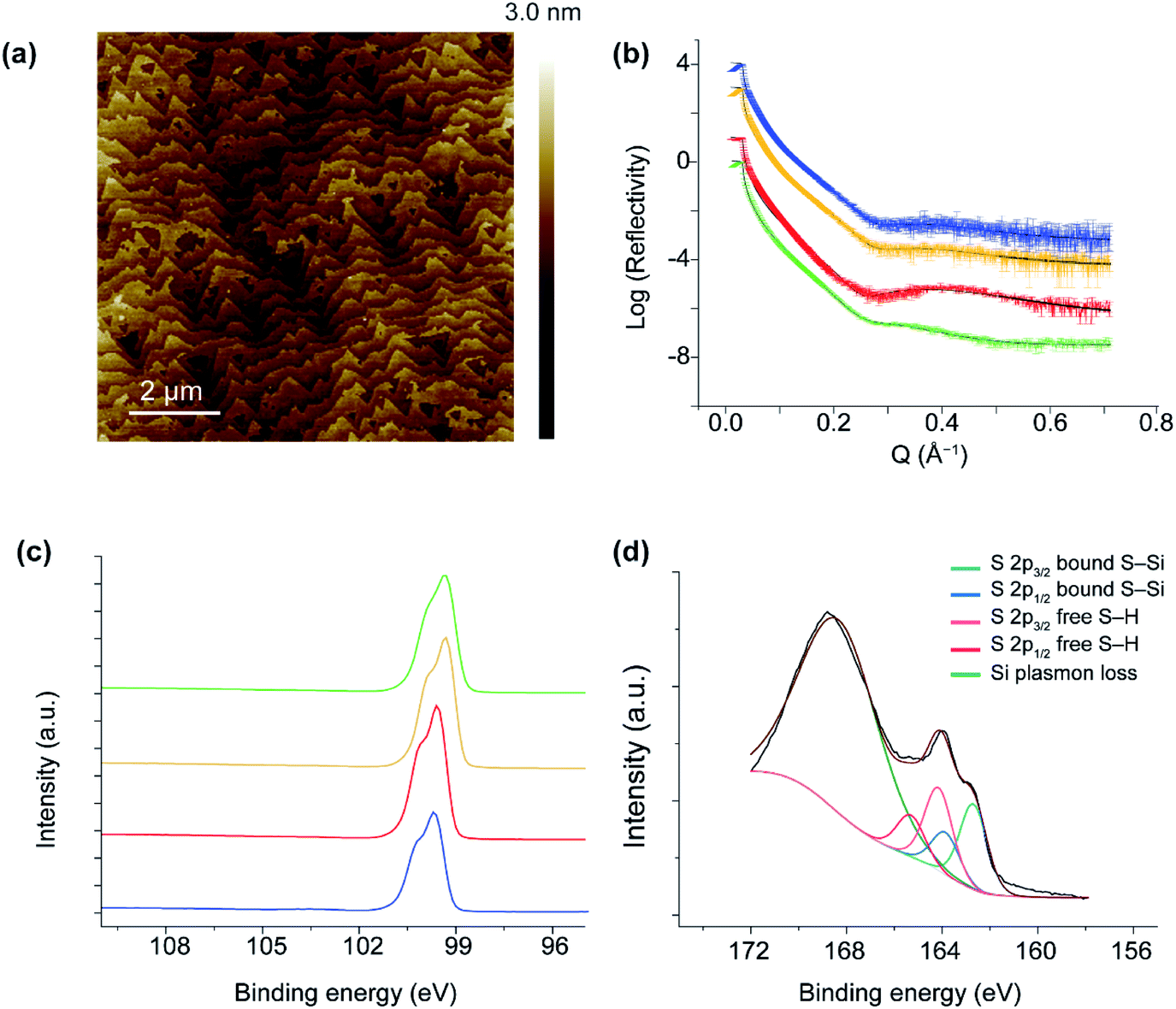 | ||
| Fig. 3 Surface characterization. (a) 10 × 10 μm2 of a p-type Si(111)–H surface covered by dithiol 2 on Si(111). (b) XRR measurements of 2 on Si(111)–H for various silicon dopant levels: high p-doped (green), low n-doped (red), low p-doped (yellow) and high n-doped (blue). The symbols with error bars are the collected data and the solid lines are the fits to each data set. The data is offset for clarity (c) XPS spectra showing the absence of Si–Ox at 102–104 eV for SAMs of 2 on high p-doped (green), low p-doped (yellow), low n-doped (red) and high n-doped (blue). The data is offset for clarity. (d) S 2p narrow XPS scan of monolayers of 2 on Si (p-type, 0.001 Ω cm). Two sets of spin–orbit-split S 2p peaks (2p1/2 and 2p3/2, high and low binding energy, respectively), held 1.16 eV apart, are evident between 162 and 165 eV. The intensity ratio between the 3/2 and 1/2 emission is set to two, and values of full width at half maximum are 1.3 eV. The S 2p emission centred at 164.7 eV is ascribed to thiols in a R–SH configurations, and the emission 163.3 eV is associated to thiols bound to Si (RS–Si). | ||
The mechanical stability under electric fields of the monolayers were assessed by conductive AFM measurements using peak force tunneling mode (PF-TUNA) tip-induced local oxidation method. The topography and current–voltage (I–V) data show that unmodified bare H-terminated silicon can be oxidized by applying 2 V for a period of 8 min. In contrast, surface covered with a SAM of 2 provides a robust barrier to surface oxidation up to 2 V (see Fig. S2, ESI†).
2.4 SAM characterization by XPS and XRR
The reflection of applied X-rays to a SAM of 2 on p-type and n-type Si is shown in Fig. 3b, from which the thickness and surface coverage can be approximately extracted, see Section 2, ESI.† For Si(111)–H, the adsorbate volume fraction is estimated to be from 0.878 to 0.981. This corresponds to 5.36–6.64 × 10¹⁴ molecules cm−2, indicating 68–84% coverage. Averaging over four samples of different doping levels, the coverage is 75 ± 8%. The apparent height of the SAM is given in Tables S1 and S2, ESI,† ranging from 8.5–11.1 Å. The height variation is due to the differences in surface coverage, the perceived surface roughness, and the angle of the molecules from the surface. Later DFT calculations perceive the C–C chain propagation direction as being closely parallel to the vector from the surface-bound Si atom to the distant S atom, a vector of length 11.1 Å at low coverage and 11.4 Å at 1:1 coverage. If the angle of chain propagation from the surface face is θ, then the SAM height is ca. 11.1 sinθ. Using this relationship, the average chain angle obtained from this data is 66 ± 16°, in rough agreement with previous measurements for alkanethiol SAMs on Si(111)–H of 57° for dodecanethiol,75 75° for octadecanethiol,64 and 60 ± 2° for hexanethiol and larger alkanethiols.79
XPS analyses of monolayers of 2 showed two sets of spin–orbit-split (SOS) S 2p1/2 and S 2p3/2 peaks, each 1.18 eV apart (Fig. 3d). The SOS emissions at 162.7 eV and 163.9 eV correspond to S–Si bonding, whilst the emissions at 164.17 eV and 165.35 eV correspond to the distal free SH of 2. The ratio of the two sets of SOS is 0.49:0.51 for the bound versus free thiol, respectively, indicating that the molecules do not hairpin and therefore do not bind with both thiols attached to the Si surface. The peak at 168 eV is attributed to Si plasmon loss.80 The absence of peaks in the 102–104 eV range indicate that negligible oxides or sub-oxides are present, a requirement of a well-formed monolayer that historically has not been expected when O2 is present under reaction conditions.21,27,29,64,65,75,79
2.5 DFT understanding of the SAM formation process
DFT calculations for the test reagent C3H7SH attacking a Si(111)–H surface, represented as a 3 × 3 supercell, produced no indication of a reaction pathway below an activation free energy of 90 kcal mol−1. To account for the observed reaction, barrier heights must be much lower than this, presumably <20 kcal mol−1. Hence some means for enhancing the reaction is required. The observation that SAM formation is greatly retarded in oxygen-depleted solutions indicates that O2 is involved. It can act as an initiator as thiols RSH and O2 in solution react to form disulfides RSSR, species always in equilibrium with thiyl radicals RS˙ (Fig. 4a). Most significantly, this reaction consumes the available solution oxygen before it becomes exposed to silicon surfaces. DFT calculations (Fig. 4b) then indicate that thiyls react with Si(111)–H barrierlessly to abstract a surface hydrogen and form a thiol RS–H physisorbed to a silicon-surface radical site; similar reactions on silicon compounds usually have a small barrier to abstraction.81 The produced intermediate can then react quickly over a transition state free-energy barrier of 9 kcal mol−1 to form a covalent Si–S bond and a neighboring surface radical, releasing H2.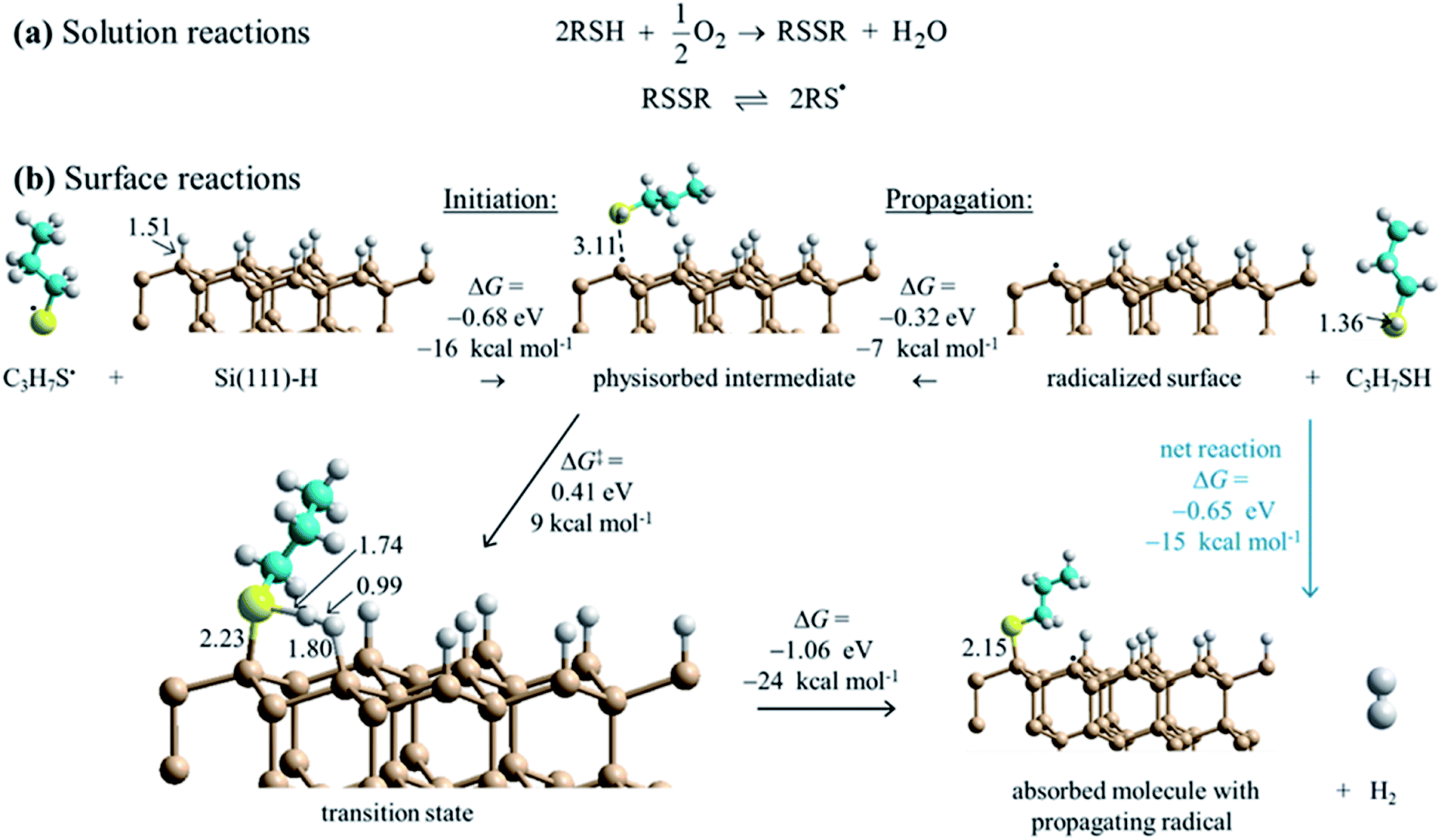 | ||
| Fig. 4 Proposed reaction scheme for the consumption of ambient oxygen as an initiator leading to surface free-radical polymerization. (a) Known solution reactions of thiols (RSH). (b) DFT mechanism for surface SAM formation starting at low coverage. Calculations indicate that thiyl radicals (RS˙, with here R = C3H7) react with Si(111)–H to abstract hydrogen to form thiol physisorbed to a silicon surface radical (black dot). Reaction over a barrier then leads to chemisorption and radical regeneration. This provides initiation for a free-radical polymerization reaction that then covers the surface with adsorbate. Some critical bond lengths are shown, in Å; only one copy of the used 3 × 3 supercell is shown. These results show Gibbs free energy changes for surface reactions, while ESI Fig. S3† provides analogous electronic energy changes, with detailed internal reaction coordinate descriptions provided in ESI Fig. S6.† Also, ESI Fig. S4 and S5† provide analogous energies for a model compound. | ||
The calculations indicate that thiols can barrierlessly react with silicon surface radicals, either a pre-existing radical or else one produced by the above thiyl attack. In either case, Fig. 4 shows that this leads to a similar physisorbed intermediate and the same chemical reaction, making a new product surface radical. Hence, thiyl attachment can be considered as an initiation reaction for a subsequent free-radical polymerization process. The net free-energy change of the propagation reaction at low coverage is calculated to be −24 kcal mol−1. In simpler terms, the net reaction occurs owing to the different bond strengths, calculated to be Si–S: 88 kcal mol−1 and H–H: 103 kcal mol−1 for the products, outcompeting Si–H: 78 kcal mol−1 and S–H: 89 kcal mol−1 for the reactants.82
2.6 SAM completion at high coverage for the binding of 2 to Si(111)–H
Progress of SAM formation up to high coverage is described in detail in Section 3 in ESI.† There, calculations on a 3 × 3 supercell for the binding of 2 to Si(111)–H depict a complicated scenario, with many possible mechanisms for the formation of irregular, kinetically trapped SAMs. Key results are presented in Fig. 5a shows a low coverage 1:9 SAM with the alkane chain at its native angle of 68° from the surface. Next, Fig. 5b shows a SAM at 7:9 coverage producible quickly by free-radical polymerization, displaying six nearly vertically aligned chains and one chain lying over at 54°. Averaging the sine of these orientations indicates an average angle of 76°, consistent the observed XRR average value of 66 ± 16°. The coverage is 78%, close to the XRR observed value of 75 ± 8%. The inter-chain separations are near their optimal value of 4.3 Å, indicating near-maximum chain density. Finally, Fig. 5c shows a SAM at full 1:1 coverage (inter-chain separation (8/3)1/2rSi–Si = 3.827 Å). The calculations indicate that increasing the coverage from 7:9 to 8:9 is endothermic, owing to increasing chain compression. A coverage of 1:1 could be producible, in principle, by repeated attack of solution thiyl radicals RS˙ on the 7:9 SAM.
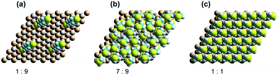 | ||
| Fig. 5 DFT calculated SAM structures for 2 on Si(111)–H as a function of coverage, showing each four copies of the 3 × 3 supercell used in the calculations. (a) 1:9, (b) 7:9, and (c) 1:1. | ||
These results are consistent with the observed qualitative chemistry. The production of regular surfaces requires 24 hours owing to the low concentration of thiyls in solution and the need for them to diffuse to the reaction sites, but, under most circumstances, regular SAMs of coverage ca. 75% coverage, e.g., the calculated 7:9 SAM, not 1:1 SAMs. In deoxygenated solutions, SAM growth can still be initiated by intrinsic surface radical defects, defects produced if there is exposure to UV light, or by most any other radical species present in solution, utilizing well-known harsh technologies.30,52,53,67,74–77 Without such harsh conditions, SAM growth is erratic and easily inhibited, producing SAMs of at most 10% coverage.
2.7 Control experiments using S–CH3 contacts
Control experiments using 3, a methyl-protected version of 1, showed that the SAM formation is not possible with thioether rather than thiol contacts (see Fig. S7–S12 in ESI†). Unlike SAMs formed with 1 or 2, Si(111)–H surfaces incubated in 4 mM solution of 3 for 24 h showed no evidence of ferrocene signals in cyclic voltammetry and no evidence of S–Si bonding in XPS. These results are consistent with the DFT mechanism in that the reaction pathway of 1 or 2 with Si (111)–H involves the formation of disulfides RSSR (Fig. 4a), which is not possible to form in the protected version of 1 (S–CH3 contacts).2.8 Single molecule STM-junction studies
The SAMs results in the previous sections demonstrate the mild conditions by which thiols are capable to covalently bond to Si electrodes. The distal thiol contacts in 2 is conserved upon attachment as shown in the XPS section, which opens the possibility of a top Si (or Au) contact to spontaneously connect, forming Si–molecule–Si circuits. We proceeded to show this by performing single-molecule measurements using the scanning tunneling microscopy (STM) junction technique in the current-time or “blinking approach”83–85 (Fig. 6a–c) in which a Si STM tip is brought within tunneling distance to a Si surface in the presence of a dilute solution of 2.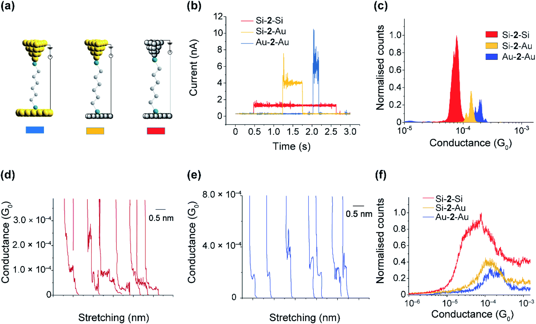 | ||
| Fig. 6 (a) Cartoons of the junctions studied. (b) Representative blinks for single molecules of 2 bonded to two Au(111) electrodes (blue), one Au(111) and one Si(111)–H electrode (yellow), and two Si(111)–H electrodes (red). (c) Blinking histograms for the Au–2–Au, Au–2–Si and Si–2–Si junctions. The blinking histograms were constructed by the accumulation of 300 blinks for each system. Each blinking histogram was normalised to the total number of blinks. (d) Representative current-distance traces for Si–2–Si junctions. (e) Representative current-distance traces for Au–2–Au junctions. (f) Current-distance traces histograms constructed from the accumulation of 3000 curves for each system. Each histogram was normalised to the total number of traces. | ||
Fig. 6a shows typical blinks of the Au–2–Au as compared to that of Au–2–Si and Si–2–Si junctions. The average conductance peaks occur at 180 μG0 (G0 = 77.4 μS and is the conductance of a single open quantum channel) for Au–2–Au junctions, 120 μG0 for Au–2–Si junctions, and 50 μG0 for Si–2–Si junctions, with both Si electrodes being p-type highly doped at 3.8 × 10¹⁹ dopant atoms per cm3. The conductivity of the junctions formed from the Si electrodes are only few folds less than those made using gold. Nevertheless, the slightly lower conductivity of Si–2–Si junctions is mild and is well within the accessible current range of typical STM-junction measurements for detecting single molecules between gold electrodes. The important advantage of the Si–2–Si junctions, however, is their enhanced mechanically stability, facilitating junctions lasting on average 5 times longer than the gold–molecule junctions. This increased “ON” lifetime will enable a range of external stimuli, such as light and electrochemical gating to be applied while a single molecule is connected between the source and drain electrodes.
Fig. 6d–f show the results obtained from the tapping method (current versus distance profiles), in which the tip is driven into and out from the surface and the current versus distance monitored. Three thousand current versus distance traces (Fig. 6d and e) were collected and accumulated into conductance histograms. The average conductance (Fig. 6f) is 170 μG0 for Au–2–Au junctions, 125 μG0 for Au–2–Si junctions, and 60 μG0 for Si–2–Si junctions, all of which are consistent with the conductance values obtained via the blinking method. Plateau length histograms for Au–2–Au and Si–2–Si junctions showed an average plateau length of 0.25 nm and 0.70 nm, respectively (Fig. S13, ESI†). This suggests that, owing to the enhanced mechanical stability, the Si–2–Si junctions are resistant to breakage during the entire pulling cycle, whereas typical Au–2–Au junctions break before a full molecular stretch.
3. Conclusions
We demonstrate that thiols can form stable covalent bonds to H-terminated silicon, leading to the nearly regular and dense SAMs, using reactions that are easy to perform and compatible with facilities available in silicon-manufacturing plants. They involve radical mechanisms, being initiated by O2 present in the reaction solvent at ambient conditions. DFT calculations indicate that thiyl radicals produced in solution by the O2 can react barrierlessly with Si(111)–H to initiate a subsequent free-radical polymerization reaction between the surface and solution thiols. They can also react with, and eliminate, SAM imperfections. The DFT results, obtained here for alkyl-radical attack on Si(111), are generally applicable for the description of many free-radical polymerization processes previously reported on Si(111)–H pertaining to the use of harsh reaction conditions.30,52,53,67,74–77 The important, unexpected, feature of the current work is that SAMs made under mild conditions in the presence of O2 do not show oxidative damage to the silicon, a feature that would limit product usefulness and hence has been, historically, rigorously excluded. This results as the oxygen is consumed by the thiols in solution, which happens before the solution is exposed to the surface.In principle, highly ordered pure alkanethiol SAMs with 1:1 coverage of adsorbate molecule to Si(111) surface sites are possible, but this requires compression of the alkane chains together, demanding specific circumstances to facilitate the compression. Observed SAM coverages of ∼75% are found, in agreement with calculated results suggesting that 7:9 is the maximum achievable coverage under normal conditions. This coverage is high enough to generate a dense, if not perfectly regular, monolayer that will prevent further reactions with the silicon surface and hence sample degradation, similar to the best SAMs produced by other means. Ferrocene-terminated alkane thiols also form very regular SAMs on Si(111) at 1:3 coverage. The monolayers are mechanically robust and resist desorption under an electric field of 2 V nm−1 opening new prospects in molecular electronics. Single-molecule Si–molecule–Si junctions are mechanically stable, owed to the strong Si–S contacts, with an average life time of 2.7 s at room temperature, which is five times higher than molecular junctions formed between the typical gold electrodes. The Si–S chemistry offers a viable way to make top/bottom contacts between semiconductors in miniaturized electronics and open prospects for a hybrid technology that merges silicon and molecular electronics.
4. Experimental methods
4.1. General chemicals and materials
All chemicals were of analytical grade and used as received. Chemicals used in surface modification and electrochemical experiments were of high purity (>99%). Hydrogen peroxide (30 wt% in water), ammonium fluoride (Puranal TM, 40 wt% in water) and sulfuric acid (Puranal TM, 95–97%) used in wafer etching and cleaning procedures were of semiconductor grade from Sigma-Aldrich. Compound 1 (98%) and 2 (98%) were purchased from Sigma-Aldrich; both were used without further purification. Synthesis of 3 is described in ESI Section 5.† Milli-Q water (>18 MΩ cm) was used to prepare electrolytes and for surface cleaning procedures. The DCM, 2-propanol, and ethanol solvents were redistilled prior to use. When required, dissolved O2 was removed from the DCM by bubbling argon for 60 min. All silicon wafers were purchased from Siltronix, S.A.S. (Archamps, France). The thickness of the wafers was 500 ± 25 μm, cut to be oriented ±0.5° away from the (100) or (111) plane. p-Type silicon was boron doped with nominal resistivity of either 0.001 Ω cm (for highly doped) or 10 Ω cm (for low doped). n-Type silicon was phosphorous doped with nominal resistivity of 0.001 Ω cm (for highly doped) or 10 Ω cm (for low doped).4.2. Thiol-functionalized silicon (100) and (111) surfaces
Assembly of 1 or 2 onto both n-type and p-type silicon proceeded as sketched in Fig. 1. Silicon wafers were cut into pieces (approximately 10 × 10 mm), cleaned for 20–30 min in hot Piranha solution (130 °C, 3:1 (v/v)) mixture of concentrated sulfuric acid to 30% hydrogen peroxide, rinsed with water and then etched with a deoxygenated 40% aqueous ammonium fluoride solution for 13 min. The freshly etched Si–H surface was then covered by a 4 mM solution of the thiol in DCM for 24 h to allow spontaneous monolayer formation. Re-distilled DCM was used to clean samples before all subsequent analyses, followed by drying under a stream of Ar gas.
4.3. Electrochemical measurements
All the electrochemical measurements were performed with a CHI650 (CH Instruments, USA) electrochemical workstation and a conventional three-electrode system with a platinum wire as the auxiliary electrode, and a silicon wafer modified with 1 as the working electrode. An Ag/AgCl aqueous electrode (3.0 M KCl, CH Instruments, USA) served as the reference.4.4. AFM measurements
Atomic force microscopy images were obtained using a Bruker dimension microscope operating in tapping mode. All images were obtained in air, at room temperature, and using silicon nitride cantilevers (TESPA from Bruker, with a spring constant of 20 N m−1). Tip induced oxide formation was carried out by conductive AFM, current–voltage data were obtained using a Bruker ICON head with Peak Force Tuna module at room temperature with Pt (RMN) probes having a spring constant of 18 N m−1. AFM–Pt tip induced SiOx oxide patterns were obtained by varying the applied bias from 0.5 V to 5 V. The resolution was set to 256 points/line, the scan rate to 1 Hz and the peak force to 554 nN. During the local oxidation, the humidity, tip scan speed, and all other parameters were kept constant, except for the applied bias voltage. The local oxidation patterns were obtained for n-type Si(111) substrates, with the surface is modified with 2. The oxidation rate of the SAM modified surface was compared to that for the Si(111)–H surface under identical conditions.4.5. X-ray photoelectron spectroscopy (XPS) and reflectometry (XRR) measurements
X-ray photoelectron spectroscopy measurements were performed on a Kratos Axis Ultra DLD spectrometer using a monochromatic Al Kα (1486.6 eV) irradiation source operating at 150 W. Spectra of Si 2p (90–110 eV), C 1s (277–300 eV), N 1s (390–410 eV) and S 2p (163–164 eV) were taken in normal emission at or below 7 × 10⁻⁹ Torr. Data files were processed using CasaXPS© software and the reported XPS energies are binding energies expressed in eV. After background subtraction (Shirley), spectra were fitted with Voigt functions. To correct for energy shifts caused by adventitious charging, all peak energies were corrected with a rigid shift to bring the C 1s emission to 285.0 eV. Specular X-ray reflectometry at the solid–air interface was conducted on a Panalytical Ltd X'Pert Pro instrument with a tube source (Cu Kα radiation, λ = 1.54 Å). The beam was focused using a Göbel mirror and collimated using fixed slits of 0.1 mm. The samples were mounted onto a motorized stage to adjust the sample into the optimal position for measurements. Angles of incidence were measured from 0.05° to 5.00° in 0.01° steps for 20 seconds per step. The raw data was reduced so that the critical edge was normalized to a reflectivity of unity and the data was presented as reflectivity versus momentum transfer, Q, which is equal to 4πsinθ/λ, where θ is the angle of incidence and λ is the X-ray wavelength (1.54 Å). Structural parameters for the monolayer were refined in MOTOFIT reflectometry analysis software.
4.6 STM break junction
STM experiments were carried out with PicoSPM 1 microscope head controlled by a “Picoscan 2500 electronics, from Agilent”. The STM-junction data were collected using an NI-DAQmx/BNC-2110 national instruments (LabVIEW data collection system) and analysed with code based on LabVIEW software.In the blinking approach, the tunnelling current is first stabilized for 1 h until tunnelling current variation of <10% is obtained. Current transients are then captured when a molecule connect between the STM tip and the surface in the presence of 4 μM solution of 2.
In the current-distance approach, the STM tip is moved in and out from a surface in the presence of the 4 μM solution of 2. 3000 current versus distance traces were collected and were all accumulated in the conductance histograms without selection.
4.7. DFT calculations
All periodic-slab calculations were performed using VASP 5.4.1, where the valence electrons were separated from the core by use of projector-augmented wave pseudopotentials (PAW) using “PREC = HIGH”. The energy tolerance for the electronic structure determinations was set at 10−7 eV to ensure accuracy. We used k-space grids of 2 × 2 × 1 for 3 × 3 supercells and 1 × 1 × 1 for 5 × 5 supercells. The PBE density functional was used, combined with Grimme's “D3” empirical dispersion correction with Becke–Johnson damping; the dispersion force is known to be important in controlling properties of SAMs containing alkane chains.15,82,86 The vacuum region between slabs was ca. 15 Å wide, with the silicon lattice vector being 5.412 Å (4/31/2 times rSi–Si = 2.34346 Å). Dipole corrections were not used. Geometry optimizations were made for all structures, terminating when the forces on all atoms fell below 0.01 eV Å−1. The slabs were 4 silicon layers thick; for 3 × 3 supercells, the lower two layers were frozen.The transition state was optimized first for a model cluster compound using Gaussian 16 (ref. 87) with the 6-31++G** basis set,88 employing Hessian matrices analytically evaluated at each step. This was then transferred onto the 2D surface and optimized using aspects of the DUSHIN vibrational analysis package,89 utilizing a numerically evaluated Hessian matrix weighted to favor coordinate updates to closely following the imaginary Hessian eigenvalue up toward the transition state at the expense of following positive eigenvalues downhill. This guarantees the rapid and smooth convergence of the VASP calculations to the transition state. Free energies were evaluated using DUSHIN for all structures based on standard approaches.90
4.8. STM tip preparation
Silicon STM tips were mechanically cut from double-side polished silicon wafers oriented on the (〈111〉 ± 0.05°) and of thickness 180 μm using a diamond cutter into ca. 3 mm size tips. Ohmic contact to the tips was made by connecting a gold wire 2 mm away from the apex of the tip. The gold wire connector serves as the connection to the STM scanner. The tips were then washed with DCM, 2-propanol, Milli-QTM water and cleaned for 30 min in hot Piranha solution (130 °C, a 3:1 (v/v) mixture of concentrated sulfuric acid to 30% hydrogen peroxide), rinsed with water and dried under a stream of Ar gas. Gold wires were then connected to the tips using gallium-indium eutectic to form an ohmic contact and conductive adhesive (Anders) to give mechanical stability. The tips were then etched in 3.50 M KOH solution at 65 °C for 48 h. The silicon tips were then dipped in a 40% solution of NH4F for 5 min to remove any remaining oxide and to expose Si–H at the apex of the tip. Tip apexes radius of <1 μm was consistently obtained using the above method and is comparable to the mechanically cut gold STM tips routinely used in STM break junction experiments. Scanning electron-microscopy (SEM) images of the silicon tips are shown in Fig. S14d–f, ESI.† Similar images for the gold STM tips used are shown in Fig. S14a–c, ESI.†
Conflicts of interest
There are no conflicts to declare.Acknowledgements
We thank the Australian Research Council for grants DE160101101 and DE160100732. We also thank the National Natural Science Foundation of China (NSFC; Grant No. 11674212), and the Shanghai High-End Foreign Experts Grant for funding this research, as well as National Computational Infrastructure and Intersect. We thank Dr Jean-Pierre Veder from the John de Laeter Centre for the assistance with XPS measurements.Notes and references
- H. Rieley and G. K. Kendall, Langmuir, 1999, 15, 8867 CrossRef CAS.
- J. C. Love, L. A. Estroff, J. K. Kriebel, R. G. Nuzzo and G. M. Whitesides, Chem. Rev., 2005, 105, 1103 CrossRef CAS PubMed.
- G. Heimel, L. Romaner, E. Zojer and J. L. Brédas, Nano Lett., 2007, 7, 932 CrossRef CAS PubMed.
- J. G. Van Alsten, Langmuir, 1999, 15, 7605 CrossRef CAS.
- H. Haick and Y. Paz, J. Phys. Chem. B, 2003, 107, 2319 CrossRef CAS.
- C. Vericat, M. E. Vela, G. Benitez, P. Carro and R. C. Salvarezza, Chem. Soc. Rev., 2010, 39, 1805 RSC.
- A. Vilan, D. Aswal and D. Cahen, Chem. Rev., 2017, 117, 4248 CrossRef CAS PubMed.
- N. Darwish, P. K. Eggers, S. Ciampi, Y. Tong, S. Ye, M. N. Paddon-Row and J. J. Gooding, J. Am. Chem. Soc., 2012, 134, 18401 CrossRef CAS PubMed.
- A. H. Pakiari and Z. Jamshidi, J. Phys. Chem. A, 2010, 114, 9212 CrossRef CAS PubMed.
- A. Vilan and D. Cahen, Chem. Rev., 2017, 117, 4624 CrossRef CAS PubMed.
- J. R. Reimers, M. J. Ford, A. Halder, J. Ulstrup and N. S. Hush, Proc. Natl. Acad. Sci. U. S. A., 2016, E1424 CrossRef CAS PubMed.
- J. R. Reimers, M. J. Ford, S. M. Marcuccio, J. Ulstrup and N. S. Hush, Nat. Rev. Chem., 2017, 1, 1 CrossRef.
- N. Darwish, P. K. Eggers, S. Ciampi, Y. Zhang, Y. Tong, S. Ye, M. N. Paddon-Row and J. J. Gooding, Electrochem. Commun., 2011, 13, 387 CrossRef CAS.
- Y. Wang, Q. J. Chi, J. D. Zhang, N. S. Hush, J. R. Reimers and J. Ulstrup, J. Am. Chem. Soc., 2011, 133, 14856 CrossRef CAS PubMed.
- J. Yan, R. Ouyang, P. S. Jensen, E. Ascic, D. A. Tanner, B. Mao, J. Zhang, C. Tang, N. S. Hush, J. Ulstrup and J. R. Reimers, J. Am. Chem. Soc., 2014, 136, 17087 CrossRef CAS PubMed.
- R. Ouyang, J. Yan, P. S. Jensen, E. Ascic, S. Gan, D. Tanner, B. Mao, L. Niu, J. Zhang and C. Tang, ChemPhysChem, 2015, 16, 928 CrossRef CAS PubMed.
- C. L. McGuiness, A. Shaporenko, C. K. Mars, S. Uppili, M. Zharnikov and D. L. Allara, J. Am. Chem. Soc., 2006, 128, 5231 CrossRef CAS PubMed.
- D. Zerulla and T. Chassé, Langmuir, 2002, 18, 5392 CrossRef CAS.
- A. Vezzoli, R. J. Brooke, N. Ferri, S. J. Higgins, W. Schwarzacher and R. J. Nichols, Nano Lett., 2017, 17, 1109 CrossRef CAS PubMed.
- M. A. C. Campos, J. M. Paulusse and H. Zuilhof, Chem. Commun., 2010, 46, 5512 RSC.
- H. Sano, K. Ohno, T. Ichii, K. Murase and H. Sugimura, Jpn. J. Appl. Phys., 2010, 49, 01 Search PubMed.
- C. R. Peiris, Y. B. Vogel, A. P. Le Brun, A. C. Aragonès, M. L. Coote, I. Díez-Pérez, S. Ciampi and N. Darwish, J. Am. Chem. Soc., 2019, 141, 14788 CrossRef CAS PubMed.
- J. A. de Sousa, F. Bejarano, D. Gutiérrez, Y. R. Leroux, E. M. Nowik Boltyk, T. Junghoefer, E. Giangrisostomi, R. Ovsyannikov, M. B. Casu, J. Veciana, M. Mas-Torrent, B. Fabre, C. Rovira and N. Crivillers, Chem. Sci., 2020, 11, 516 RSC.
- B. Fabre, Chem. Rev., 2016, 116, 4808 CrossRef PubMed.
- B. Fabre and F. Hauquier, Langmuir, 2017, 33, 8693 CrossRef CAS PubMed.
- A. Vilan, O. Yaffe, A. Biller, A. Salomon, A. Kahn and D. Cahen, Adv. Mater., 2010, 22, 140 CrossRef CAS PubMed.
- G. Ashkenasy, D. Cahen, R. Cohen, A. Shanzer and A. Vilan, Acc. Chem. Res., 2002, 35, 121 CrossRef CAS PubMed.
- J. M. Buriak, Chem. Rev., 2002, 102, 1271 CrossRef CAS PubMed.
- S. R. Puniredd, O. Assad and H. Haick, J. Am. Chem. Soc., 2008, 130, 13727 CrossRef CAS PubMed.
- M. R. Linford and C. E. D. Chidsey, J. Am. Chem. Soc., 1993, 115, 12631 CrossRef CAS.
- J. W. McPherson, Microelectron. Reliab., 2012, 52, 1753 CrossRef CAS.
- L. J. Webb, D. J. Michalak, J. S. Biteen, B. S. Brunschwig, A. S. Y. Chan, D. W. Knapp, H. M. Meyer III, E. J. Nemanick, M. C. Traub and N. S. Lewis, J. Phys. Chem. B, 2006, 110, 23450 CrossRef CAS PubMed.
- K. T. Wong and N. S. Lewis, Acc. Chem. Res., 2014, 47, 3037 CrossRef CAS PubMed.
- O. Assad and H. Haick, IEEE Int. Symp. Ind. Electron., 2008, 2040–2044 Search PubMed.
- M. Dasog, K. Bader and J. G. C. Veinot, Chem. Mater., 2015, 27, 1153 CrossRef CAS.
- A. Fermi, M. Locritani, G. Di Carlo, M. Pizzotti, S. Caramori, Y. Yu, B. A. Korgel, G. Bergamini and P. Ceroni, Faraday Discuss., 2015, 185, 481 RSC.
- W. Peng, S. M. Rupich, N. Shafiq, Y. N. Gartstein, A. V. Malko and Y. J. Chabal, Chem. Rev., 2015, 115, 12764 CrossRef CAS PubMed.
- W. J. I. Debenedetti, S. K. Chiu, C. M. Radlinger, R. J. Ellison, B. A. Manhat, J. Z. Zhang, J. Shi and A. M. Goforth, J. Phys. Chem. C, 2015, 119, 9595 CrossRef CAS.
- O. S. Kang, J. P. Bruce, D. E. Herbert and M. S. Freund, ACS Appl. Mater. Interfaces, 2015, 7, 26959 CrossRef CAS PubMed.
- J. Wang, Y. Zhou, M. Watkinson, J. Gautrot and S. Krause, Sens. Actuators, 2015, 209, 230 CrossRef CAS.
- M. Dasog, J. Kehrle, B. Rieger and J. G. C. Veinot, Angew. Chem., Int. Ed., 2016, 55, 2322 CrossRef CAS PubMed.
- E. S. Brown, S. Hlynchuk and S. Maldonado, Surf. Sci., 2016, 645, 49 CrossRef CAS.
- A. A. Yasseri, D. Syomin, R. S. Loewe, J. S. Lindsey, F. Zaera and D. F. Bocian, J. Am. Chem. Soc., 2004, 126, 15603 CrossRef CAS PubMed.
- F. Peng, Y. Su, Y. Zhong, C. Fan, S. T. Lee and Y. He, Acc. Chem. Res., 2014, 47, 612 CrossRef CAS PubMed.
- X. Cheng, S. B. Lowe, P. J. Reece and J. J. Gooding, Chem. Soc. Rev., 2014, 43, 2680 RSC.
- L. H. Yu, N. Gergel-Hackett, C. D. Zangmeister, C. A. Hacker, C. A. Richter and J. G. Kushmerick, J. Phys.: Condens. Matter, 2008, 20, 374114 CrossRef PubMed.
- S. Ciampi, M. H. Choudhury, S. A. B. A. Ahmad, N. Darwish, A. L. Brun and J. J. Gooding, Electrochim. Acta, 2015, 186, 216 CrossRef CAS.
- Y. B. Vogel, L. Zhang, N. Darwish, V. R. Gonçales, A. Le Brun, J. J. Gooding, A. Molina, G. G. Wallace, M. L. Coote, J. Gonzalez and S. Ciampi, Nat. Commun., 2017, 8, 2066 CrossRef PubMed.
- A. C. Aragonès, N. Darwish, S. Ciampi, F. Sanz, J. J. Gooding and I. Diéz-Pérez, Nat. Commun., 2017, 8, 15056 CrossRef PubMed.
- A. Allain, J. Kang, K. Banerjee and A. Kis, Nat. Mater., 2015, 14, 1195 CrossRef CAS PubMed.
- H. Sugimura, in Nanocrystalline Materials: Their Synthesis-Structure-Property Relationships and Applications, ed. S.-C. Tjong, Elsevier, 2nd edn, 2013, p. 161 Search PubMed.
- A. B. Sieval, A. L. Demirel, J. W. M. Nissink, M. R. Linford, J. H. Van Der Maas, W. H. De Jeu, H. Zuilhof and E. J. R. Sudhölter, Langmuir, 1998, 14, 1759 CrossRef CAS.
- J. M. Buriak and M. D. H. Sikder, J. Am. Chem. Soc., 2015, 137, 9730 CrossRef CAS PubMed.
- J. M. Buriak, M. P. Stewart, T. W. Geders, M. J. Allen, H. C. Choi, J. Smith, D. Raftery and L. T. Canham, J. Am. Chem. Soc., 1999, 121, 11491 CrossRef CAS.
- E. J. Nemanick, P. T. Hurley, L. J. Webb, D. W. Knapp, D. J. Michalak, B. S. Brunschwig and N. S. Lewis, J. Phys. Chem. B, 2006, 110, 14770 CrossRef CAS PubMed.
- E. G. Robins, M. P. Stewart and J. M. Buriak, Chem. Commun., 1999, 2479 RSC.
- R. Boukherroub, A. Petit, A. Loupy, J. N. Chazalviel and F. Ozanam, J. Phys. Chem. B, 2003, 107, 13459 CrossRef CAS.
- A. I. A. Soliman, T. Utsunomiya, T. Ichii and H. Sugimura, Langmuir, 2018, 34, 13162 CrossRef CAS PubMed.
- Q. Y. Sun, L. C. P. M. de Smet, B. van Lagen, M. Giesbers, P. C. Thüne, J. van Engelenburg, F. A. de Wolf, H. Zuilhof and E. J. R. Sudhölter, J. Am. Chem. Soc., 2005, 127, 2514 CrossRef CAS PubMed.
- Q. Y. Sun, L. C. P. M. de Smet, B. van Lagen, A. Wright, H. Zuilhof and E. J. R. Sudhölter, Angew. Chem., Int. Ed., 2004, 43, 1352 CrossRef CAS PubMed.
- S. K. Coulter, M. P. Schwartz and R. J. Hamers, J. Phys. Chem. B, 2001, 105, 3079 CrossRef CAS.
- Y. H. Lai, C. T. Yeh, C. C. Yeh and W. H. Hung, J. Phys. Chem. B, 2003, 107, 9351 CrossRef CAS.
- C. A. Hacker, Solid-State Electron., 2010, 54, 1657 CrossRef CAS.
- B. Bhartia, S. R. Puniredd, S. Jayaraman, C. Gandhimathi, M. Sharma, Y. C. Kuo, C. H. Chen, V. J. Reddy, C. Troadec and M. P. Srinivasan, ACS Appl. Mater. Interfaces, 2016, 8, 24933 CrossRef CAS PubMed.
- Y. B. Vogel, L. Zhang, N. Darwish, V. R. Gonçales, A. Le Brun, J. J. Gooding, A. Molina, G. G. Wallace, M. L. Coote and J. Gonzalez, Nat. Commun., 2017, 8, 2066 CrossRef PubMed.
- N. Gergel-Hackett, C. D. Zangmeister, C. A. Hacker, L. J. Richter and C. A. Richter, J. Am. Chem. Soc., 2008, 130, 4259 CrossRef CAS PubMed.
- M. Hu, F. Liu and J. M. Buriak, ACS Appl. Mater. Interfaces, 2016, 8, 11091 CrossRef CAS PubMed.
- Y. S. Huang, C. H. Chen, C. H. Chen and W. H. Hung, ACS Appl. Mater. Interfaces, 2013, 5, 5771 CrossRef CAS PubMed.
- M. C. Walkey, C. R. Peiris, S. Ciampi, A. C. Aragonès, R. B. Domínguez-Espíndola, D. Jago, T. Pulbrook, B. W. Skelton, A. N. Sobolev and I. Díez Pérez, ACS Appl. Mater. Interfaces, 2019, 11, 36886 CrossRef CAS PubMed.
- A. I. A. Soliman, T. Ichii, T. Utsunomiya and H. Sugimura, Soft Matter, 2015, 11, 5678 RSC.
- H. G. Steinrück, A. Schiener, T. Schindler, J. Will, A. Magerl, O. Konovalov, G. Li Destri, O. H. Seeck, M. Mezger, J. Haddad, M. Deutsch, A. Checco and B. M. Ocko, ACS Nano, 2014, 8, 12676 CrossRef PubMed.
- J. W. McPherson and H. C. Mogul, J. Appl. Phys., 1998, 84, 1513 CrossRef CAS.
- A. B. Sieval, R. Linke, H. Zuilhof and E. J. R. Sudhölter, Adv. Mater., 2000, 12, 1457 CrossRef CAS.
- M. Hu, T. C. Hauger, B. C. Olsen, E. J. Luber and J. M. Buriak, J. Phys. Chem. C, 2018, 122, 13803–13814 CrossRef CAS.
- J. L. Lou, H. W. Shiu, L. Y. Chang, C. P. Wu, Y. L. Soo and C. H. Chen, Langmuir, 2011, 27, 3436 CrossRef CAS PubMed.
- M. R. Linford, P. Fenter, P. M. Eisenberger and C. E. D. Chidsey, J. Am. Chem. Soc., 1995, 117, 3145 CrossRef CAS.
- A. B. Sieval, R. Opitz, H. P. A. Maas, M. G. Schoeman, G. Meijer, F. J. Vergeldt, H. Zuilhof and E. J. R. Sudhölter, Langmuir, 2000, 16, 10359 CrossRef CAS.
- A. Faucheux, A. C. Gouget-Laemmel, C. Henry de Villeneuve, R. Boukherroub, F. Ozanam, P. Allongue and J. N. Chazalviel, Langmuir, 2006, 22, 153 CrossRef CAS PubMed.
- L. Y. Chang, Y. C. Kuo, H. W. Shiu, C. H. Wang, Y. C. Lee, Y. W. Yang, S. Gwo and C. H. Chen, Langmuir, 2017, 33, 14244 CrossRef CAS PubMed.
- F. M. Hassan, R. Batmaz, J. Li, X. Wang, X. Xiao, A. Yu and Z. Chen, Nat. Commun., 2015, 6, 8597 CrossRef CAS PubMed.
- A. A. Zavitsas and C. Chatgilialoglu, J. Am. Chem. Soc., 1995, 117, 10645 CrossRef CAS.
- J. R. Reimers, D. Panduwinata, J. Visser, Y. Chin, C. Tang, L. Goerigk, M. J. Ford, M. Sintic, T. J. Sum and M. J. J. Coenen, Proc. Natl. Acad. Sci. U. S. A., 2015, 112, E6101 CrossRef CAS PubMed.
- R. J. Nichols and S. J. Higgins, Nat. Mater., 2015, 14, 465 CrossRef CAS PubMed.
- R. J. Nichols, W. Haiss, S. J. Higgins, E. Leary, S. Martin and D. Bethell, Phys. Chem. Chem. Phys., 2010, 12, 2801 RSC.
- A. C. Aragones, N. L. Haworth, N. Darwish, S. Ciampi, N. J. Bloomfield, G. G. Wallace, I. Diez-Perez and M. L. Coote, Nature, 2016, 531, 88 CrossRef CAS PubMed.
- H. H. Arefi, M. Nolan and G. Fagas, Langmuir, 2014, 30, 13255 CrossRef CAS PubMed.
- M. J. Frisch, G. W. Trucks, H. B. Schlegel, G. E. Scuseria, M. A. Robb, J. R. Cheeseman, G. Scalmani, V. Barone, G. A. Petersson, H. Nakatsuji, X. Li, M. Caricato, A. V. Marenich, J. Bloino, B. G. Janesko, R. Gomperts, B. Mennucci, H. P. Hratchian, J. V. Ortiz, A. F. Izmaylov, J. L. Sonnenberg, D. Williams, F. Ding, F. Lipparini, F. Egidi, J. Goings, B. Peng, A. Petrone, T. Henderson, D. Ranasinghe, V. G. Zakrzewski, J. Gao, N. Rega, G. Zheng, W. Liang, M. Hada, M. Ehara, K. Toyota, R. Fukuda, J. Hasegawa, M. Ishida, T. Nakajima, Y. Honda, O. Kitao, H. Nakai, T. Vreven, K. Throssell, J. A. Montgomery Jr, J. E. Peralta, F. Ogliaro, M. J. Bearpark, J. J. Heyd, E. N. Brothers, K. N. Kudin, V. N. Staroverov, T. A. Keith, R. Kobayashi, J. Normand, K. Raghavachari, A. P. Rendell, J. C. Burant, S. S. Iyengar, J. Tomasi, M. Cossi, J. M. Millam, M. Klene, C. Adamo, R. Cammi, J. W. Ochterski, R. L. Martin, K. Morokuma, O. Farkas, J. B. Foresman and D. J. Fox, Gaussian 16 Revision B.01, Gaussian Inc., Wallingford, CT, 2016 Search PubMed.
- W. J. Hehre, R. Ditchfield and J. A. Pople, J. Chem. Phys., 1972, 56, 2257 CrossRef CAS.
- J. R. Reimers, J. Chem. Phys., 2001, 115, 9103 CrossRef CAS.
- J. W. Ochterski, Thermochemistry in GAUSSIAN, Gaussian Inc., 2000, http://www.gaussian.com/g_whitepap/thermo/thermo.pdf Search PubMed.
Footnote |
| † Electronic supplementary information (ESI) available: Additional experimental and computational characterisation, including coordinates of optimized structures. See DOI: 10.1039/d0sc01073a |
| This journal is © The Royal Society of Chemistry 2020 |