
 Open Access Article
 This Open Access Article is licensed under a Creative Commons Attribution-Non Commercial 3.0 Unported Licence
D–π–D molecular semiconductors for perovskite solar cells: the superior role of helical versus planar π-linkers†
Niansheng
Xu
,
Aibin
Zheng
,
Yuefang
Wei
,
Yi
Yuan
*,
Jing
Zhang
,
Ming
Lei
 and
Peng
Wang
*
and
Peng
Wang
*
Department of Chemistry, Zhejiang University, Hangzhou 310028, China. E-mail: yyuan@zju.edu.cn; pw2015@zju.edu.cn
First published on 24th February 2020
Abstract
Controlling the mode of molecular packing and the size of molecular aggregates is of fundamental importance for high-performance charge transport materials in next-generation optoelectronic devices. To clarify the peculiar role of helicene as a kernel block in the exploration of unconventional organic semiconductors, in this work thia[5]helicene (T5H) is doubly aminated with electron-donating dimethoxydiphenylamine to afford T5H–OMeDPA, which is systematically compared with its perylothiophene (PET) congener (PET–OMeDPA). On the basis of the quantum theory of atoms in molecules and energy decomposition analysis of single crystals, it is surprisingly found that while π–π stacking of planar PET is stronger than that of helical T5H, this desirable effect for the charge transport of organic semiconductors is completely lost for donor–π–donor (D–π–D) type PET–OMeDPA but is retained for T5H–OMeDPA to a large extent. Consequently, the T5H–OMeDPA single-crystal presents about 5 times higher theoretical hole-mobility than PET–OMeDPA. More critically, the solution-processed racemic glassy film of T5H–OMeDPA displays a 3 times higher hole-mobility in comparison with the PET–OMeDPA counterpart, due to a larger domain of molecular aggregates. With respect to PET–OMeDPA, there is a weaker electronic coupling of helical T5H–OMeDPA with perovskites, leading to reduced interfacial charge recombination. Due to reduced transport resistance and enhanced recombination resistance, perovskite solar cells with T5H–OMeDPA exhibit a power conversion efficiency of 21.1%, higher than 19.8% with PET–OMeDPA and 20.6% with the spiro-OMeTAD control.
1. Introduction
Helicenes are a class of ortho-fused aromatic polycycles, where the conjoined rings are unable to exist in the same plane, resulting in an intrinsically helical shape.1,2 Consequently, helicenes are found in both right-handed and left-handed chiral (so-called enantiomeric) forms. This helically chiral architecture, coupled with their fully conjugated structure, endow these molecules with strong circular dichroism. Helicene can be used as a circularly polarized (CP) emissive material and in CP-photodiodes.3–5 Furthermore, nonplanar aromatic systems of helicenes possess curved or twisted π-surfaces. While nonplanar molecules show a variety of fascinating molecular packing arrangements with respect to planar molecules, the curved π-electron system often disturbs π–π stacking, which is desirable for self-assembly or semiconducting materials utilizing the intermolecular electronic interaction.6 Contorting the molecules allows new types of intermolecular contacts to emerge and in some cases can enhance intermolecular charge transfer.7 In particular, racemic helicenes have great potential for the growth of single crystals featuring multi-dimensional charge transport. In 2004, Rajca et al. reported a racemic single crystal of thia[7]helicene, with the characteristic of two-dimensional charge transport.8 In 2015, Itami et al. synthesized a double helicene with three-dimensional lamellar packing.9Actually, an organic semiconducting layer in light-emitting diodes or solar cells is always amorphous.10 Since intermolecular charge hopping is more efficient within ordered domains than across grain boundaries and through disordered domains, charge-carrier mobility will depend heavily on the size of the ordered domain. In 2017, a racemic thin film of 1-aza[6]helicene was reported by Fuchter et al. to display a larger domain of molecular aggregates, affording an 80-fold higher hole mobility in comparison with the enantiopure counterpart.11 Later, Gao et al. reported a binaphthol derivative based racemic thin film, presenting a larger grain size and a nearly 2 orders of magnitude higher electron mobility than the enantiopure one.12
Lead halide based perovskite solar cells (PSCs) have stimulated much recent research interest as they could evolve into a cost-effective photovoltaic technology with great promise.13–15 For a high-efficiency PSC with the n–i–p device configuration, a hole transport layer (HTL) is needed with excellent film-forming ability, suitable energy levels, and high conductivity.16–30 In 2014, Wakamiya et al. reported a nonplanar oxygen-bridged triarylamine, displaying high carrier mobility in the π-stacking direction even in an amorphous thin film.31 Later, they developed an oxygen-bridged triarylamine substituted azulene for PSC application.32 Recently we reported a racemic glassy film composed of bis(4-methoxyphenyl)amine functionalized oxa[5]helicene (O5H–OMeDPA) as a donor–π–donor (D–π–D) type HTL for efficient PSCs.33 Meanwhile, we are also curious to know whether a helicene based organic semiconductor is really superior to its planar counterpart. However the preparation of the perylo[1,12-bcd]furan (PEF) counterpart seems infeasible due to the lack of mature synthetic conditions for PEF. In this paper, we will start from thia[5]helicene (T5H) to synthesize an O5H–OMeDPA analogue, N5,N5,N9,N9-tetrakis(4-methoxyphenyl)dinaphtho[2,1-b:1′,2′-d]thiophene-5,9-diamine (T5H–OMeDPA, Fig. 1A), with a motivation to fundamentally compare it with the perylo[1,12-bcd]thiophene (PET) counterpart, N3,N3,N10,N10-tetrakis(4-methoxyphenyl)perylo[1,12-bcd]thiophene-3,10-diamine (PET–OMeDPA, Fig. 1A).
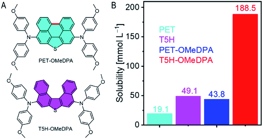 | ||
| Fig. 1 (A) Chemical structures of two D–π–D molecular semiconductors consisting of the π-linkers of PET and T5H in combination with the electron-donor of OMeDPA: PET–OMeDPA and T5H–OMeDPA. With respect to T5H–OMeDPA, the only one extra covalent bond in PET–OMeDPA is marked with red color. (B) Solubilities of PET, T5H, PET–OMeDPA, and T5H–OMeDPA in chlorobenzene. | ||
2. Results and discussion
2.1. Synthesis, solubility, and thermal properties
As presented in the ESI,† PET–OMeDPA and T5H–OMeDPA can be readily prepared with PET (ref. 34) and T5H (ref. 35) as the respective starting materials, via double bromination and Buchwald–Hartwig C–N cross-coupling. The chemical structures of target molecules were preliminarily determined by nuclear magnetic resonance spectroscopy and high-resolution mass spectrometry (Fig. S22–S27†). For solution-processing of an organic semiconducting thin film, molecular solubility plays a crucial role in determining the surface morphology and film thickness. The solubility of T5H in chlorobenzene is measured as 49.1 mM (Fig. 1B), which is over twice higher than 19.1 mM for the planar PET counterpart. This can be facilely explained by the contorted geometry of T5H, which should be good for solvation. Derivation of T5H from 4,4′-dimethoxydiphenylamine further pushes the solubility to 188.5 mM for T5H–OMeDPA, which is over four times higher than 43.8 mM for PET–OMeDPA. This feature stimulates our interest in the design of helicene based molecular semiconductors also without using flexible aliphatic chains. As shown in Fig. S1†, T5H–OMeDPA has a glass transition temperature (Tg) of 138 °C, which is slightly higher than 131 °C for PET–OMeDPA.2.2. Single-crystal structure and intermolecular interaction
To gain a fundamental understanding of the microscopic packing of PET–OMeDPA and T5H–OMeDPA molecules in perfectly ordered solids compared to PET (ref. 36) and T5H,37 single crystals suitable for X-ray analysis were grown via slow evaporation of nearly saturated solutions in a solvent mixture of dichloromethane and heptane. All kinds of dimers were further extracted from single-crystal structures to figure out the intermolecular noncovalent interactions (NCI), which underlie the self-organization of molecules, by theoretical calculations on the basis of the quantum theory of atoms in molecules (QTAIM) and energy decomposition analysis (EDA).38,39 The details of molecular packing and NCI analysis of PET and T5H single crystals are presented in Fig. S2–S5.†While the molecule in the PET single crystal is coplanar (Fig. S2†), it is very interesting to note from Fig. 2A that the π-linker in PET–OMeDPA no longer exists as a plane. As shown in Fig. S6†, the PET π-linker is actually convex or concave, affording two enantiomers. PET–OMeDPA crystallizes in a triclinic P![[1 with combining macron]](https://www.rsc.org/images/entities/char_0031_0304.gif) space group with two head-to-head enantiomers in a primitive unit cell (Table S1†). As shown in Fig. S7†, PET–OMeDPA molecules in the ac plane can be concisely described with IH4 isohedral tiling.40 Along the crystallographic b axis one can simply translate the double layer found in the ac plane (Fig. 2B) to generate a three-dimensional structure.
space group with two head-to-head enantiomers in a primitive unit cell (Table S1†). As shown in Fig. S7†, PET–OMeDPA molecules in the ac plane can be concisely described with IH4 isohedral tiling.40 Along the crystallographic b axis one can simply translate the double layer found in the ac plane (Fig. 2B) to generate a three-dimensional structure.
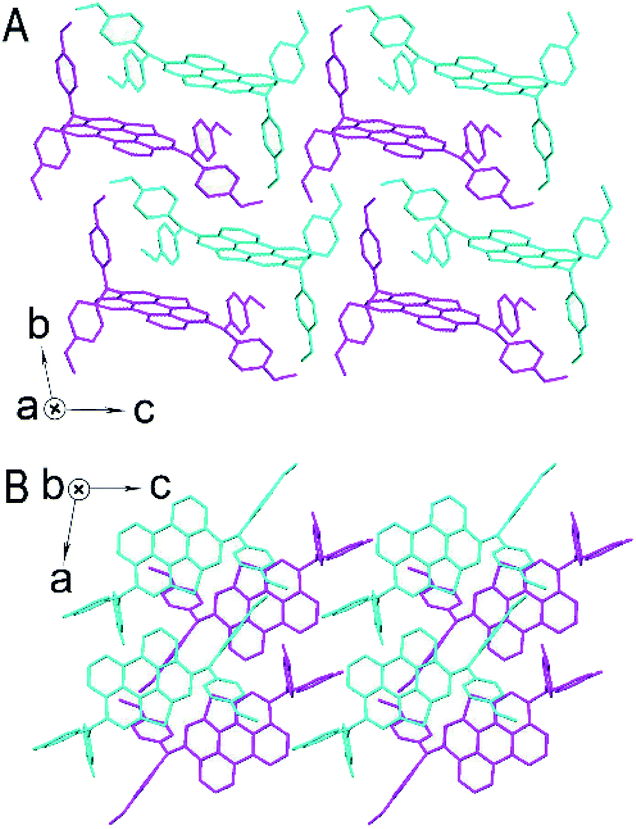 | ||
| Fig. 2 Single-crystal structures of PET–OMeDPA viewed from the crystallographic a axis (A) and the b axis (B). Two enantiomers extracted from the crystallographic analysis, with the π-linker of PET being convex and concave, are marked in magenta and cyan. Hydrogen atoms are omitted for clarity. | ||
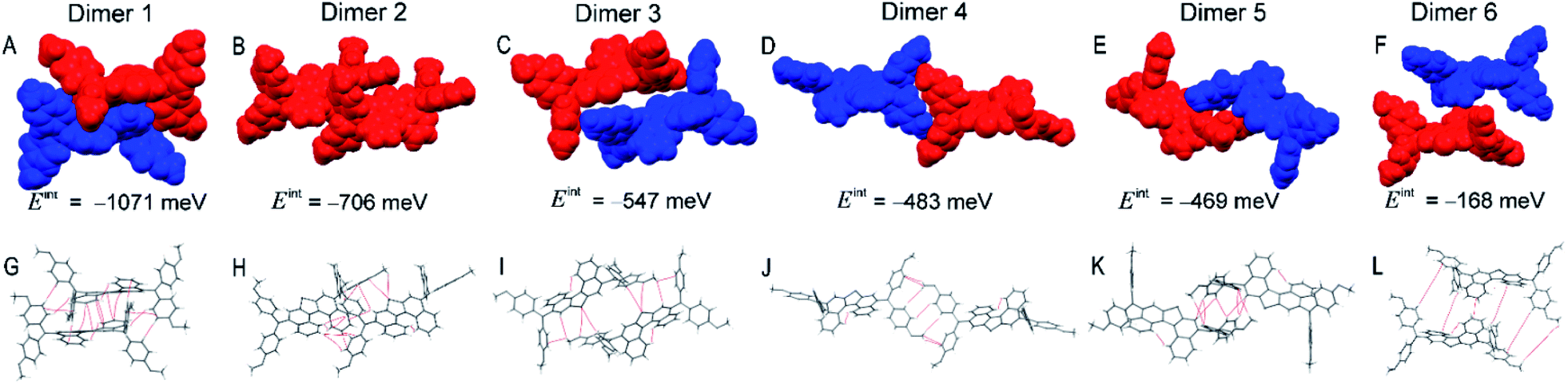
As shown in Fig. 3, dimer 1 in a primitive unit cell has the largest Eint value of 1032 meV among the six dimers in the PET–OMeDPA crystal. Dimer 2 and dimer 3 with comparable Eint values of 703 meV and 692 meV are acquired along the a axis, dimer 4 with Eint = 626 meV along the b axis, dimer 5 with Eint = 568 meV along the c axis, and dimer 6 with Eint = 545 meV along the [110] direction. The Eint values in various directions are not significantly disparate, contributing to the comparable lengths (Table S1†) in the three dimensions of the single crystal.
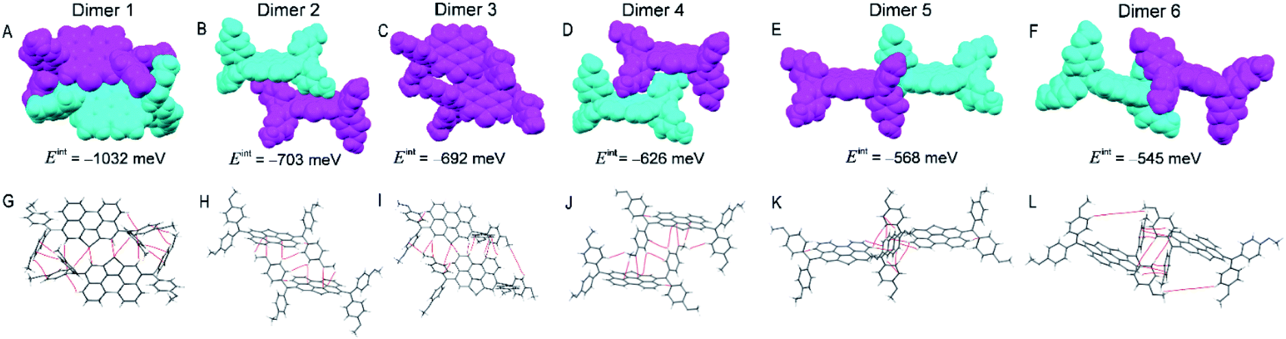 | ||
| Fig. 3 (A–F) Space-filling packing structures of dimers 1–6 selected from the PET–OMeDPA single-crystal. (G–L) Molecular graphs elaborating on intermolecular interactions. The covalently bonded atoms are additionally linked via a “bond path” (marked in red), a line along which electron density is maximal. The “bond path” is used here for the depiction of non-covalent interactions in a dimer. The total interaction energy (Eint) is calculated by energy decomposition analysis. | ||
Multiple NCIs can be found from Fig. 3G–L for the PET–OMeDPA single-crystal, including six forms of CH⋯π interactions between: (i) the PET aromatic CH and the methoxyphenyl (MeOPhen) π-skeleton (dimer 3); (ii) the PET aromatic CH and the PET π-skeleton (dimers 2, 3, 5, and 6); (iii) the MeOPhen aromatic CH and the MeOPhen π-skeleton (dimers 1, 2, 4, and 6); (iv) the MeOPhen aromatic CH and the PET π-skeleton (dimers 1, 4, 5, and 6); (v) the MeOPhen aliphatic CH and the PET π-skeleton (dimer 2); (vi) the MeOPhen aliphatic CH and the MeOPhen π-skeleton (dimer 3), two types of S⋯π interactions between: (vii) the PET sulfur atoms and the PET π-skeleton (dimer 1); (viii) the PET sulfur atoms and the MeOPhen π-skeleton (dimer 3), one kind of O⋯π interaction between (ix) the MeOPhen oxygen atoms and the PET π-skeleton (dimers 2 and 4), one kind of CH–S interaction between (x) the MeOPhen aromatic CH and the PET sulfur atom (dimers 1 and 3), one kind of CH–O interaction between (xi) the PET aromatic CH and the MeOPhen oxygen atom (dimer 3), and four kinds of H–H interactions between: (xii) the PET aromatic CH and the MeOPhen aromatic CH (dimer 5); (xiii) of the MeOPhen aromatic CH (dimer 2); (xiv) the MeOPhen aliphatic CH and the PET aromatic CH (dimer 3); (xv) the MeOPhen aliphatic CH and the MeOPhen aromatic CH (dimers 1, 3, 4, and 6). Note that different from PET, the face-to-face π⋯π interaction does not exist at all in the PET–OMeDPA single-crystal.
The T5H–OMeDPA single-crystal is categorized into the triclinic P space group with two face-to-face, antiparallel enantiomers in a primitive unit cell. As shown in Fig. S8,† we can differentiate one enantiomer from another by discriminating the helicity (M-type or P-type) of the T5H π-linker. In the single-crystal, the T5H π-linker of T5H–OMeDPA distorts with a torsional angle of 42.6°, which is slightly smaller than that of T5H (44.2°). As shown in Fig. 4A, along the crystallographic b and c axes there is an alternating arrangement of enantiomers M and P. The projection of T5H–OMeDPA molecules in the bc plane matches well with IH47 isohedral tiling (Fig. S9†).40 The double layer in the bc plane (Fig. 4B) can be translated along the crystallographic a axis to build a three-dimensional structure.
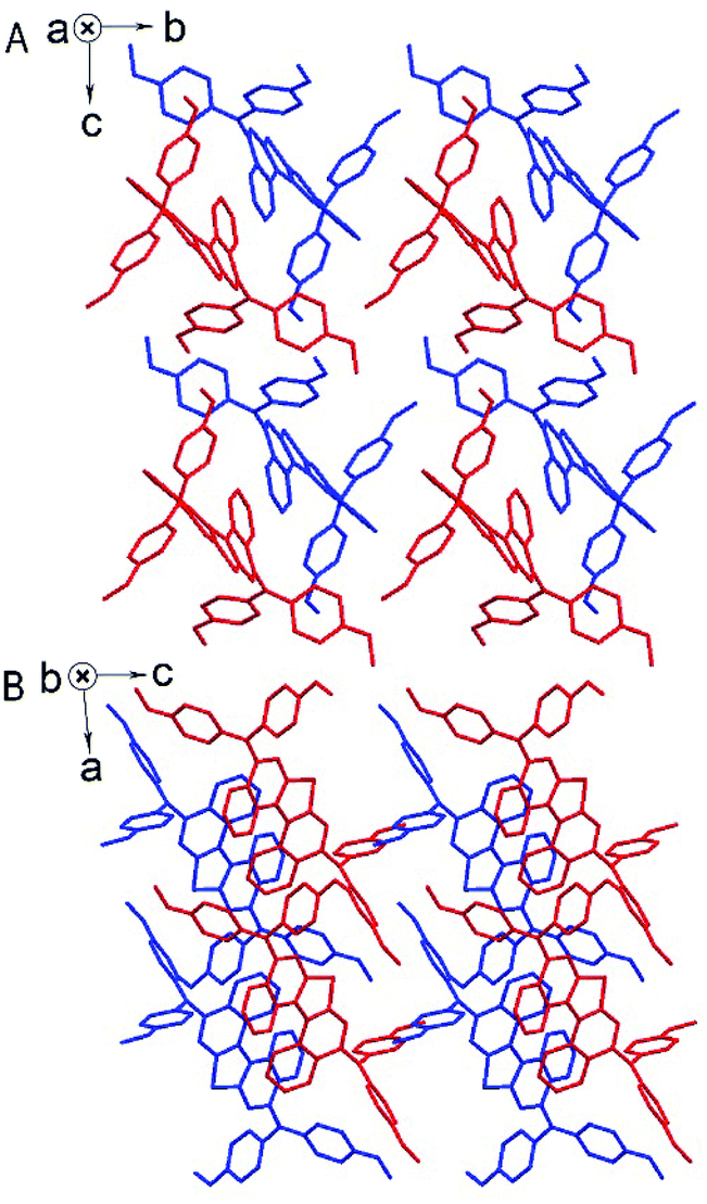 | ||
| Fig. 4 Crystal structures of T5H–OMeDPA from the crystallographic a (A) and b (B) axes. Two enantiomers with the π-linker of T5H categorized as M-type helicene and P-type helicene are marked in blue and red, respectively. Hydrogen atoms are omitted. | ||
The Eint value of dimer 1 consisting of a primitive unit cell of T5H–OMeDPA is calculated as 1071 meV, which is much larger compared to those of the other five dimers. Dimer 2 with Eint = 706 meV and dimer 3 with Eint = 547 meV are both identified along the a axis, dimer 4 with Eint = 483 meV along the [101] direction, dimer 5 with Eint = 469 meV along the c axis, and dimer 6 with Eint = 168 meV along the b axis. In general, the Eint values of dimers 2 and 3, which are formed with adjacent molecules belonging to two primitive unit cells along the a axis, are larger than those of the counterparts (dimers 4 and 6) in the bc plane, which is probably the intrinsic origin of the growth of single-crystalline microwires (Table S1†).
For T5H–OMeDPA single-crystal, multiple NCIs can be identified from Fig. 5G–L including three kinds of π⋯π interactions between: (i) the T5H aromatic π-skeleton and the T5H aromatic π-skeleton (dimers 5 and 6); (ii) the T5H π-skeleton and the MeOPhen aromatic π-skeleton (dimer 2); (iii) the MeOPhen π-skeleton and the MeOPhen π-skeleton (dimer 1), four types of CH⋯π interactions between: (iv) the T5H aromatic CH and the MeOPhen π-skeleton (dimer 2); (v) the MeOPhen aromatic CH and the T5H π-skeleton (dimers 1 and 5); (vi) the MeOPhen aromatic CH and the MeOPhen π-skeleton (dimers 2, 3, and 6); (vii) the MeOPhen aliphatic CH and the MeOPhen π-skeleton (dimer 4), one kind of S⋯π interaction between (viii) the T5H sulfur atom and the MeOPhen π-skeleton (dimers 2 and 3), two kinds of CH–S interactions between: (ix) the T5H aromatic CH and the T5H sulfur atom (dimer 1); (x) the MeOPhen aliphatic CH and the T5H sulfur atom (dimer 2), one type of S⋯O interaction between (xi) the T5H sulfur atom and the MeOPhen oxygen atom (dimer 3), and five kinds of H–H interactions between: (xii) the T5H aromatic CH and the MeOPhen aromatic CH (dimers 1, 2, 3, 5, and 6); (xiii) the MeOPhen aromatic CH and the MeOPhen aromatic CH (dimers 1 and 4); (xiv) the MeOPhen aliphatic CH and the T5H aromatic CH (dimers 5 and 6); (xv) the MeOPhen aliphatic CH and the MeOPhen aromatic CH (dimer 4); (xvi) the MeOPhen aliphatic CH and the MeOPhen aliphatic CH (dimers 5 and 6).
 | ||
| Fig. 5 (A–F) Dimers 1–6 selected from the T5H–OMeDPA single-crystal. (G–L) Bond paths and total interaction energy (Eint). | ||
As listed in Table S3,† the total Eint value of one central molecule with all of its seven neighbors is 4.86 eV for PET–OMeDPA, which is larger than 4.15 eV for T5H–OMeDPA. This scenario coincides with the tendency of melting points: 306 °C for PET–OMeDPA and 296 °C for T5H–OMeDPA.
2.3. Electronic structure
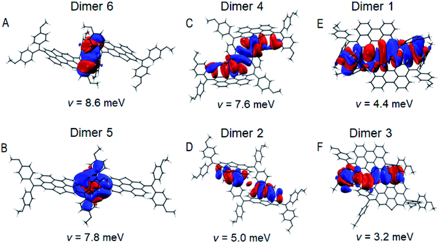
The Marcus electron transfer theory41 and density functional theory (DFT) are resorted to gain insights into the microscopic hole-transport mechanism. For calculation details, see ESI.† The computed reorganization energies (λ) and transfer integrals (v) are compiled in Tables S4–S7.†In the PET–OMeDPA single-crystal, the HOMO overlaps of adjacent OMeDPA units belonging to two molecules are observed for dimer 6 and dimer 5 from Fig. 6A and B, which have relatively large v values of 8.6 meV and 7.8 meV, respectively. In Fig. 6C and D, HOMO overlaps of MeOPhen and the PET π-linker are visualized for dimer 4 with v = 7.6 meV and dimer 2 with v = 5.0 meV. As shown in Fig. 6E and F, the HOMO overlap for dimer 1 composed of two head-to-head oriented molecules is larger than that of dimer 3 with two head-to-tail oriented molecules, which affords v values of 4.4 meV and 3.2 meV, respectively. With respect to PET, the calculated theoretical hole mobility of the PET–OMeDPA single crystal is reduced by three orders of magnitude, being 6.1 × 10⁻³ cm2 V−1 s−1 (Table S6).†
 | ||
| Fig. 6 (A–F) Isodensity surface plots of intermolecular HOMO overlaps of dimers 1–6 in the PET–OMeDPA single-crystal. The isodensity value is set at 1 × 10⁻⁶. The red and blue isosurfaces refer to the same and opposite phase overlap, respectively. | ||
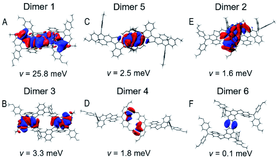
It is valuable to note that the λ value of T5H–OMeDPA is 294 meV (Table S7†), which is similar to 331 meV for PET–OMeDPA (Table S6†). Dissimilar to the situation for PET–OMeDPA, a remarkable HOMO overlap due to π⋯π stacking of the T5H linker is observed for dimer 1 of T5H–OMeDPA in Fig. 7A. The v value of dimer 1 amounts to 25.8 meV, which makes the greatest contribution to the theoretically predicted mobility of 3.3 × 10⁻² cm2 V−1 s−1 (Table S7†) for the T5H–OMeDPA single-crystal. As for the other dimers, the HOMO overlaps are attenuated (Fig. 7), and their v values remarkably drop to below 3.4 meV. As shown in Fig. 7B and E, HOMO overlaps of OMeDPA and the T5H π-linker are observed for dimer 3 and dimer 2 with v values of 3.3 meV and 1.6 meV, respectively. In dimers 4 and 5, HOMO overlaps are mainly located on the OMeDPA moiety. As shown in Fig. 7F, sparse HOMO overlap for dimer 6 occurs on the adjacent T5H π-linker, which affords a tiny v value of 0.1 meV.
 | ||
| Fig. 7 (A–F) Isodensity surface plots of intermolecular HOMO overlaps of dimers 1–6 in the T5H–OMeDPA single-crystal. | ||
The electronic band structures (Fig. S10–S12†) of PET, T5H, PET–OMeDPA, and T5H–OMeDPA single crystals were further calculated at the DFT/GGA-PW91 level. The HOMO involved band structures are presented in Fig. 8 to shed light on hole transport characteristics along various directions. For the PET single-crystal with four molecules in a primitive unit cell, the HOMO valence band consists of four π-sub-bands, which are nearly degenerate owing to the peculiar molecular orientation and HOMO profile (Fig. 8A). The HOMO valence band has a dispersion of 650 meV in the C–E, A–X, and Y–D sections of the first Brillouin zone, all of which correspond to the crystallographic b axis. Almost no dispersion is noticed in other sections. This scenario is consistent with the much larger v value of dimer 1 compared to the other dimers. In short, one-dimensional hole transport characteristics of the PET single-crystal can be readily perceived from Fig. 8A.
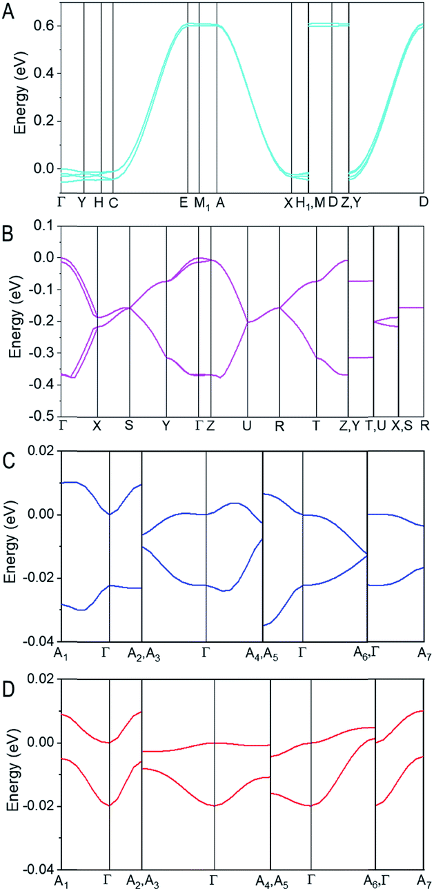 | ||
| Fig. 8 The HOMO valence band (VB) structures of single crystals calculated at the DFT/GGA-PW91 level of theory: PET (A), T5H (B), PET–OMeDPA (C), and T5H–OMeDPA (D). In the band graphic, points of high symmetry in the first Brillouin zone are as follows. PET: Γ = (0, 0, 0), A = (−0.5, 0.5, 0), C = (−0.5, 0, 0.5), D = (0, 0.5, 0.5), E = (−0.5, 0.5, 0.5), H = (−0.3733, 0, 0.6521), H1 = (−0.6267, 0, 0.3497), M = (−0.3733, 0.5, 0.6521), M1 = (−0.6267, 0.5, 0.3479), X = (−0.5, 0, 0), Y = (0, 0, 0.5), and Z = (0, 0.5, 0). T5H: Γ = (0, 0, 0), R = (0.5, 0.5, 0.5), S = (0, 0.5, 0.5), T = (0.5, 0.5, 0), U = (0.5, 0, 0.5), X = (0, 0, 0.5), Y = (0, 0.5, 0), and Z = (0.5, 0, 0). PET–OMeDPA and T5H–OMeDPA: Γ = (0, 0, 0), A1 = (0, 0.5, −0.5), A2 = (0, 0, −0.5), A3 = (0.5, −0.5, −0.5), A4 = (0.5, 0, −0.5), A5 = (0, −0.5, 0), A6 = (−0.5, 0.5, 0), and A7 = (−0.5, 0, 0). The energy levels are shifted with respect to the VB edge at the Γ point, which is set at 0 eV. | ||
Furthermore, the HOMO valence band of the T5H single-crystal presented in Fig. 8B also contains four π-sub-bands with pairwise degeneration, in agreement with four molecules in its primitive unit cell. The top-most sub-band has a dispersion of 187 meV in the section of Γ–X, which is to a first approximation connected with the largest v value of 118 meV for dimer 1 packing along the c axis. A reduced band dispersion of 73 meV in the Y–Γ section occurs with dimer 2, which piles up along the b axis with a v value of 29 meV. The almost flat band in the Γ–Z section results from a stack of dimer 4 (v= 2.2 meV) along the a axis. Different from PET, the single-crystal of T5H has a characteristic of quasi-two-dimensional hole transport, as seen in Fig. 8B.
For the HOMO valence band of the PET–OMeDPA single-crystal (Fig. 8C), two π-sub-bands exhibit a near mirror symmetry, with <40 meV energy differences in the various directions of reciprocal space. The top sub-band is nearly flat in the Γ–A7 direction with the lowest dispersion of 3.6 meV, which can be ascribed to the smallest v value of dimer 3. The dispersion of these two sub-bands in other sections is around 8 meV.
The HOMO valence band of the T5H–OMeDPA single-crystal also splits into two nearly degenerate sub-bands (Fig. 8D), with a smaller bandwidth of 30 meV in comparison with PET–OMeDPA. Even if dimer 1 has a sizable v value of 25.8 meV, no significant band dispersion can be found in all reciprocal directions, owing to the relatively small v values of the other dimers which leads to off-diagonal disorder. The dispersion of the top sub-band is about 10 meV in the Γ–A2 and Γ–A7 directions, which is relevant to the v values for dimers 3 and 5.
2.4. Hole mobility of the spun thin film
To assess the thin film hole mobilities of PET–OMeDPA and T5H–OMeDPA, which are more relevant to the diode operation, we fabricated hole-only devices with a structure of indium tin oxide|PEDOT:PSS|HTL|Au. Note that the thin films spun from chlorobenzene are blent with LiTFSI and TBP and further air-doped overnight. The thickness of the PET–OMeDPA thin film is 90 nm, which is comparable to 85 nm for the T5H–OMeDPA film. The fabrication procedure of hole-only devices is described in the ESI.† On the basis of the space-charge limited current model, the derived average thin film hole mobility is 6.26 × 10⁻⁴ cm2 V−1 s−1 for T5H–OMeDPA, which is three times higher than 1.97 × 10⁻⁴ cm2 V−1 s−1 for PET–OMeDPA (Fig. 9A). Circular dichroism measurements have proved that the solution-deposited films are racemic (Fig. S13†).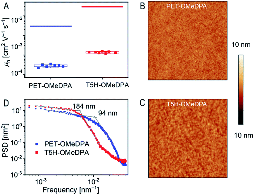 | ||
| Fig. 9 (A) Hole-mobilities derived from space-charge limited current measurements of PET–OMeDPA and T5H–OMeDPA thin films with additives (LiTFSI and TBP). The top solid lines give theoretical mobilities of single crystals. (B and C) AFM height images (5 μm × 5 μm) of thin films spun on the PEDOT:PSS substrate. (D) Plots of single-dimensional isotropic power spectral density (PSD) as a function of spatial frequency. | ||
As shown in Fig. 9B and C, a smooth and uniform thin film of either PET–OMeDPA or T5H–OMeDPA can be solution-deposited on the substrate of PEDOT:PSS. However, for the T5H–OMeDPA thin film larger domains can be clearly perceived. To define the lateral correlation length, we further carried out power spectral density analysis of the AFM images. As shown in Fig. 9D, the lateral correlation length of 184 nm for the T5H–OMeDPA thin film is much larger than 94 nm for the PET–OMeDPA counterpart. The augmented aggregate domain is favorable for charge transport in the amorphous thin film. Moreover, one can notice from Fig. 9A that due to the reduced molecular ordering, the measured hole mobility of a glassy thin film is greatly reduced by over one order of magnitude, in comparison with the theoretical value computed on the basis of the single crystal structure.
2.5. Hole extraction
We then measured static photoluminescence (PL) spectra to evaluate the yields of hole extraction (ϕh) by PET–OMeDPA and T5H–OMeDPA from a (FAPbI3)0.875(MAPbBr3)0.075(CsPbI3)0.05(PbI2)0.03 based perovskite, which is abbreviated as CsMAFA in the following discussion. The CsMAFA film deposited on glass was used as a reference. Sample preparation is detailed in the ESI.†ϕh can be estimated by | (1) |
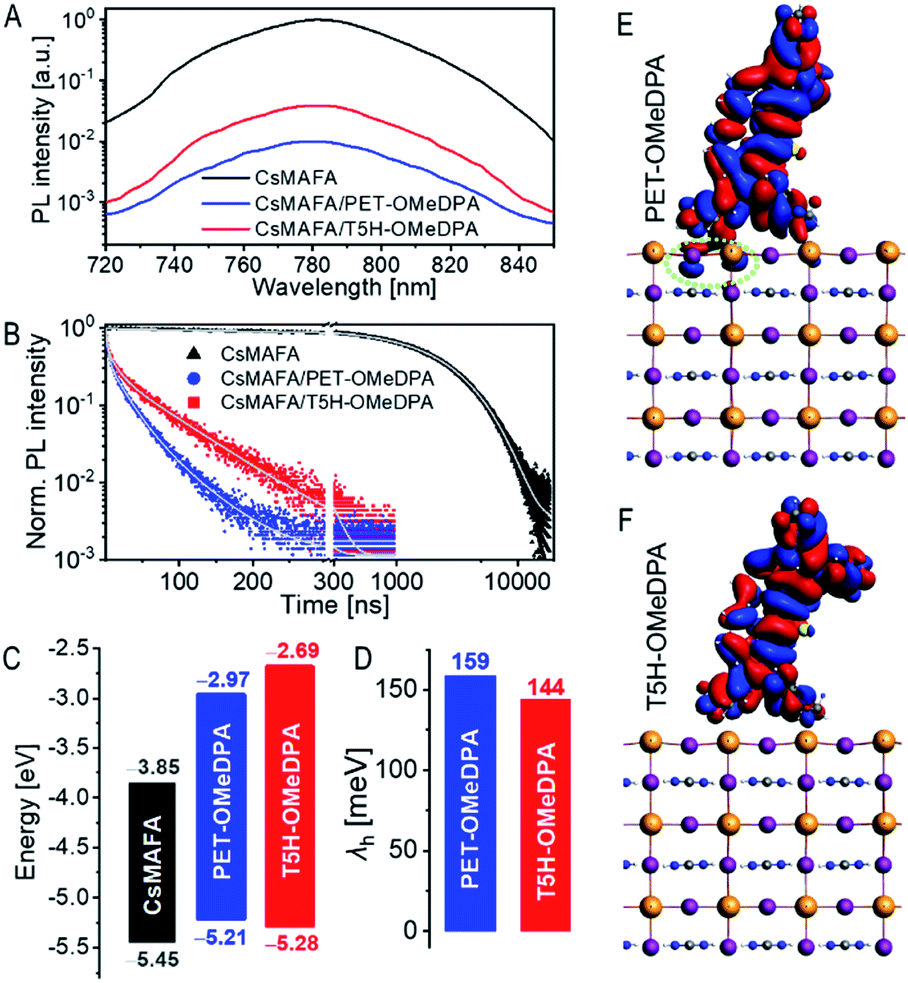 | ||
| Fig. 10 (A) Steady-state photoluminescence (PL) spectra and (B) time-resolved PL traces of a pristine perovskite film deposited on a mesoporous alumina film and the counterparts covered with PET–OMeDPA and T5H–OMeDPA. (C) Energy diagram of a CsMAFA perovskite, PET–OMeDPA, and T5H–OMeDPA. (D) Reorganization energy of hole extraction with PET–OMeDPA and T5H–OMeDPA. (E and F) Isodensity surface plots of HOMOs of optimized PET–OMeDPA and T5H–OMeDPA at the surface of a perovskite slab. The isodensity value is set at 0.005. The extension of the HOMO of PET–OMeDPA into the perovskite is highlighted with a green circle in panel E. | ||
Next, time-correlated single-photon counting measurements were executed to define the time constants of hole extraction (τh) via the equation
 | (2) |
In the context of Marcus electron transfer theory,41 the rate constant of hole extraction (τh) can be described to a good approximation as
 | (3) |
From the onset (Ei) and cutoff (Ecutoff) energy regions of ultraviolet photoelectron spectra (Fig. S14†), we obtained the energy levels of the valence band edge (or HOMO) of thin films on fluorine-doped tin oxide (FTO), being −5.45 eV versus vacuum for CsMAFA, −5.21 eV for PET–OMeDPA, and −5.28 eV for T5H–OMeDPA. The energy levels of the conduction band edge (or LUMO) are further reckoned in conjunction with optical gaps, being −3.85 eV for CsMAFA, −2.97 eV for PET–OMeDPA, and −2.69 eV T5H–OMeDPA (Fig. S15†). The energy diagram is presented in Fig. 10C. The driving force for hole extraction with PET–OMeDPA is calculated as 240 meV, which is 70 meV larger than 170 meV with T5H–OMeDPA. The reorganization energy (λh) is composed of the internal reorganization energy and the external reorganization energy. The external part can be ignored because of its negligible contribution in the solid state. By using the DFT method, the reorganization energy is calculated as 159 meV for PET–OMeDPA, which is 15 meV larger than 144 meV for T5H–OMeDPA (Fig. 10D). Therefore, for PET–OMeDPA the larger λh will partially offset the positive effect of the larger driving force. Electronic coupling between the HTL and perovskite was also computed by the DFT method. As shown in Fig. S16,† both PET–OMeDPA and T5H–OMeDPA interact with the FAPbI3 perovskite slab via methoxyphenyl groups. It is valuable to note from Fig. 10E that the HOMO of PET–OMeDPA expands into FAPbI3 to a small extent (marked in green circle). Thereby, it can be concluded that the reduced driving force and the weakened electronic coupling jointly bring forth slower hole extraction with T5H–OMeDPA.
2.6. Application in solar cells
We finally employed PET–OMeDPA and T5H–OMeDPA as HTLs to make PSCs with a typical device architecture: FTO|compact TiO2|mesoporous TiO2 filled with CsMAFA|CsMAFA|HTL|Au, as illustrated in Fig. 11A. The details of cell fabrication are provided in the ESI.† As observed from the AFM height images (Fig. S17A and B†), the surface of the perovskite can be nicely covered with both PET–OMeDPA and T5H–OMeDPA. Note from Fig. S17C† that the pristine perovskite layer is characterized by more distinct grain boundaries and remarkably larger roughness.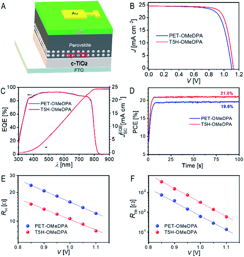 | ||
| Fig. 11 (A) Schematic of PSCs. (B) J–V curves under 100 mW cm−2, simulated AM1.5G sunlight of typical PSCs with PET–OMeDPA and T5H–OMeDPA. (C) EQE curves and integrated JSC over the standard AM1.5G spectrum. (D) PCE output via MPP tracking. (E) Plots of hole transport resistance (RH) as a function of potential bias (V). (F) Charge recombination resistance (Rre). The solid lines in panels E and F are shown as a guide to the eye. | ||
Photocurrent density–voltage (J–V) curves of typical devices with PET–OMeDPA and T5H–OMeDPA were measured under irradiation with simulated air mass 1.5 global sunlight (AM1.5G, 100 mW cm−2) and are collected in Fig. 11B. The PET–OMeDPA based PSC has a short-circuit current (JSC) of 24.58 mA cm−2, an open-circuit voltage (VOC) of 1.100 V, and a fill factor (FF) of 0.732, resulting in a power conversion efficiency (PCE) of 19.8%. In contrast, the cell using T5H–OMeDPA displays an improved open-circuit voltage (VOC) of 1.125 V and an increased fill factor (FF) of 0.764, leading to a higher PCE of 21.1% along with a similar JSC of 24.60 mA cm−2. As shown in Fig. S18†, negligible hysteresis exists for PET–OMeDPA and T5H–OMeDPA based cells. Also note from Fig. S19† that a control cell which was fabricated under the same conditions as spiro-OMeTAD (state-of-the-art hole-transporter) presents a PCE of 20.6%. As shown in Fig. S20†, the dispersions of photovoltaic parameters (JSC, VOC, FF, and PCE) are pretty small for two batches of 10 cells.
Plots of the external quantum efficiency (EQE) as a function of the wavelength of incident monochromatic light are presented in Fig. 11C, predicting integrated current densities of ∼24.3 mA cm−2 under the AM1.5G conditions for both cells, which are in good accordance with the JSC values derived from J–V measurements. Furthermore, maximum power point tracking under AM1.5G illumination provides a steady-state PCE output of 21.0% and 19.6% (Fig. 11D) for PSCs with T5H–OMeDPA and PET–OMeDPA, respectively.
To shed light on the higher VOC and FF observed for the T5H–OMeDPA cell, we also recorded impedance spectra (Fig. S21A†) at a series of forward potential biases (V) and used a simplified equivalent circuit (Fig. S21B†) to derive two key physical parameters, transport resistance (RH) in the HTL and charge recombination resistance (Rre) at the interface of the perovskite and hole-transporter.42 As shown in Fig. 11E, the T5H–OMeDPA cell features a lower RH at a given V, echoing the higher mobility of its HTL (Fig. 9A) compared to the PET–OMeDPA congener, which is intrinsically linked with the improvement of the FF.
At the same V, the Rre value of the T5H–OMeDPA cell is over four times larger than that of the PET–OMeDPA counterpart (Fig. 11F), contributing to the enhancement of both VOC and FF in terms of the photodiode function depicting the Shockley equivalent circuit.43 The Rre augmentation is partly associated with a lower hole density in the HTL injected from the gold electrode, owing to the stabilized HOMO energy level of T5H–OMeDPA. Moreover, the weaker electronic coupling between T5H–OMeDPA and the perovskite (Fig. 10E and F) should also contribute to the attenuation of charge recombination.
3. Conclusions
In summary, we have employed planar PET and helical T5H as π-linkers to construct two structurally simple D–π–D type molecular semiconductors PET–OMeDPA and T5H–OMEDPA for perovskite solar cells. Crystallographic analysis and theoretical calculations have revealed that the T5H–OMeDPA single-crystal where π–π stacking of the π-linker is retained to a large extent, possesses about 5 times higher hole-mobility in contrast to the PET–OMeDPA counterpart with π–π stacking completely lost. Moreover, the solution-processed thin film of T5H–OMeDPA also displays a larger domain of molecular aggregates and therefore a 3 times higher hole-mobility than the PET–OMeDPA counterpart. Photoluminescence measurements have suggested that both T5H–OMeDPA and PET–OMeDPA can efficiently extract holes from the photoexcited perovskite film. With respect to PET–OMeDPA, T5H–OMeDPA can be used to fabricate more efficient perovskite solar cells with improved hole transport and attenuated charge recombination. Further molecular design should foster the application of helicene-based molecular semiconductors with good solution-processability and high charge-mobility for device applications.Conflicts of interest
There are no conflicts to declare.Acknowledgements
We express our sincere gratitude to the National Natural Science Foundation of China (No. 91733302, 51673165, and 21975219), the National 973 Program (2015CB932204), the Key Technology R&D Program (BE2014147-1) of Science and Technology Department of Jiangsu Province, and H. Glass.Notes and references
- Y. Shen and C.-F. Chen, Chem. Rev., 2012, 112, 1463–1535 CrossRef PubMed.
- M. Gingras, Chem. Soc. Rev., 2013, 42, 1051–1095 RSC.
- Y. Yang, R. C. da Costa, M. J. Fuchter and A. J. Campbell, Nat. Photonics, 2013, 7, 634–638 CrossRef CAS.
- J. R. Brandt, X. Wang, Y. Yang, A. J. Campbell and M. J. Fuchter, J. Am. Chem. Soc., 2016, 138, 9743–9746 CrossRef CAS PubMed.
- T. Biet, K. Martin, J. Hankache, N. Hellou, A. Hauser, T. Bürgi, N. Vanthuyne, T. Aharon, M. Caricato, J. Crassous and N. Avarvari, Chem.–Eur. J., 2017, 23, 437–446 CrossRef CAS PubMed.
- C. Nuckolls, T. J. Katz and L. Castellanos, J. Am. Chem. Soc., 1996, 118, 3767–3768 CrossRef CAS.
- S. R. Peurifoy, T. J. Sisto, F. Ng, M. L. Steigerwald, R. Chen and C. Nuckolls, Chem. Rec., 2019, 19, 1050–1061 CrossRef CAS PubMed.
- A. Rajca, M. Miyasaka, M. Pink, H. Wang and S. Rajca, J. Am. Chem. Soc., 2004, 126, 15211–15222 CrossRef CAS PubMed.
- T. Fujikawa, Y. Segawa and K. Itami, J. Am. Chem. Soc., 2015, 137, 7763–7768 CrossRef CAS.
- J. Urieta-Mora, I. García-Benito, A. Molina-Ontoria and N. Martín, Chem. Soc. Rev., 2018, 47, 8541–8571 RSC.
- Y. Yang, B. Rice, X. Shi, J. R. Brandt, R. Correa da Costa, G. J. Hedley, D.-M. Smilgies, J. M. Frost, I. D. W. Samuel, A. Otero-de-la-Roza, E. R. Johnson, K. E. Jelfs, J. Nelson, A. J. Campbell and M. J. Fuchter, ACS Nano, 2017, 11, 8329–8338 CrossRef CAS PubMed.
- M. Chen, X. Jiao, J. Li, W. Wu, H. Xin, C. R. McNeill and X. Gao, Langmuir, 2019, 35, 6188–6195 CrossRef CAS PubMed.
- A. Kojima, K. Teshima, Y. Shirai and T. Miyasaka, J. Am. Chem. Soc., 2009, 131, 6050–6051 CrossRef CAS PubMed.
- H.-S. Kim, C.-R. Lee, J.-H. Im, K.-B. Lee, T. Moehl, A. Marchioro, S.-J. Moon, R. Humphry-Baker, J.-H. Yum, J. E. Moser, M. Graetzel and N.-G. Park, Sci. Rep., 2012, 2, 591 CrossRef PubMed.
- H. Min, M. Kim, S.-U. Lee, H. Kim, G. Kim, K. Choi, J. H. Lee and S. I. Seok, Science, 2019, 366, 749–753 CrossRef CAS PubMed.
- K. Rakstys, A. Abate, M. I. Dar, P. Gao, V. Jankauskas, G. Jacopin, E. Kamarauskas, S. Kazim, S. Ahmad, M. Grätzel and M. K. Nazeeruddin, J. Am. Chem. Soc., 2015, 137, 16172–16178 CrossRef CAS PubMed.
- M. Saliba, S. Orlandi, T. Matsui, S. Aghazada, M. Cavazzini, J.-P. Correa-Baena, P. Gao, R. Scopelliti, E. Mosconi, K.-H. Dahmen, F. De Angelis, A. Abate, A. Hagfeldt, G. Pozzi, M. Graetzel and M. K. Nazeeruddin, Nat. Energy, 2016, 1, 15017 CrossRef CAS.
- S. Paek, I. Zimmermann, P. Gao, P. Gratia, K. Rakstys, G. Grancini, M. K. Nazeeruddin, M. A. Rub, S. A. Kosa, K. A. Alamry and A. M. Asiri, Chem. Sci., 2016, 7, 6068–6075 RSC.
- Z. Hu, W. Fu, L. Yan, J. Miao, H. Yu, Y. He, O. Goto, H. Meng, H. Chen and W. Huang, Chem. Sci., 2016, 7, 5007–5012 RSC.
- B. Xu, J. Zhang, Y. Hua, P. Liu, L. Wang, C. Ruan, Y. Li, G. Boschloo, E. M. J. Johansson, L. Kloo, A. Hagfeldt, A. K.-Y. Jen and L. Sun, Chem, 2017, 2, 676–687 CAS.
- M. Zhang, G. Wang, D. Zhao, C. Huang, H. Cao and M. Chen, Chem. Sci., 2017, 8, 7807–7814 RSC.
- I. Cho, N. J. Jeon, O. K. Kwon, D. W. Kim, E. H. Jung, J. H. Noh, J. Seo, S. I. Seok and S. Y. Park, Chem. Sci., 2017, 8, 734–741 RSC.
- N. J. Jeon, H. Na, E. H. Jung, T.-Y. Yang, Y. G. Lee, G. Kim, H.-W. Shin, S. I. Seok, J. Lee and J. Seo, Nat. Energy, 2018, 3, 682–689 CrossRef CAS.
- Y. Wang, Y. Yue, X. Yang and L. Han, Adv. Energy Mater., 2018, 8, 1800249 CrossRef.
- H. Zhang, Y. Wu, W. Zhang, E. Li, C. Shen, H. Jiang, H. Tian and W.-H. Zhu, Chem. Sci., 2018, 9, 5919–5928 RSC.
- E. H. Jung, N. J. Jeon, E. Y. Park, C. S. Moon, T. J. Shin, T.-Y. Yang, J. H. Noh and J. Seo, Nature, 2019, 567, 511–515 CrossRef CAS PubMed.
- C. Shen, Y. Wu, H. Zhang, E. Li, W. Zhang, X. Xu, W. Wu, H. Tian and W.-H. Zhu, Angew. Chem., Int. Ed., 2019, 58, 3784–3789 CrossRef CAS PubMed.
- Y. Wang, W. Chen, L. Wang, B. Tu, T. Chen, B. Liu, K. Yang, C. W. Koh, X. Zhang, H. Sun, G. Chen, X. Feng, H. Y. Woo, A. B. Djurišić, Z. He and X. Guo, Adv. Mater., 2019, 31, 1902781 CrossRef PubMed.
- D. P. Tabor, V. A. Chiykowski, P. Friederich, Y. Cao, D. J. Dvorak, C. P. Berlinguette and A. Aspuru-Guzik, Chem. Sci., 2019, 10, 8360–8366 RSC.
- X. Sun, F. Wu, C. Zhong, L. Zhu and Z. Li, Chem. Sci., 2019, 10, 6899–6907 RSC.
- A. Wakamiya, H. Nishimura, T. Fukushima, F. Suzuki, A. Saeki, S. Seki, I. Osaka, T. Sasamori, M. Murata, Y. Murata and H. Kaji, Angew. Chem., Int. Ed., 2014, 53, 5800–5804 CrossRef CAS PubMed.
- H. Nishimura, N. Ishida, A. Shimazaki, A. Wakamiya, A. Saeki, L. T. Scott and Y. Murata, J. Am. Chem. Soc., 2015, 137, 15656–15659 CrossRef CAS PubMed.
- N. Xu, Y. Li, D. Ricciarelli, J. Wang, E. Mosconi, Y. Yuan, F. De Angelis, S. M. Zakeeruddin, M. Grätzel and P. Wang, iScience, 2019, 15, 234–242 CrossRef CAS PubMed.
- W. Jiang, H. Qian, Y. Li and Z. Wang, J. Org. Chem., 2008, 73, 7369–7372 CrossRef CAS PubMed.
- D. Fabbri, G. Delogu and O. De Lucchi, J. Org. Chem., 1993, 58, 1748–1750 CrossRef CAS.
- I. C. Santos, M. Almeida, J. Morgado, M. T. Duarte and L. Alcácer, Acta Crystallogr., Sect. C: Cryst. Struct. Commun., 1997, 53, 1640–1642 CrossRef.
- K. Nakahara, C. Mitsui, T. Okamoto, M. Yamagishi, J. Soeda, K. Miwa, H. Sato, A. Yamano, T. Uemura and J. Takeya, Jpn. J. Appl. Phys., 2013, 52, 05DC10 CrossRef.
- R. F. W. Bader, Chem. Rev., 1991, 91, 893–928 CrossRef CAS.
- W. D. Cornell, P. Cieplak, C. I. Bayly, I. R. Gould, K. M. Merz, D. M. Ferguson, D. C. Spellmeyer, T. Fox, J. W. Caldwell and P. A. Kollman, J. Am. Chem. Soc., 1995, 117, 5179–5197 CrossRef CAS.
- J. Simon and P. Bassoul, in Design of Molecular Materials: Supramolecular Engineering, John Wiley & Sons Inc., New York, 2000, ch. 3, pp. 90–110 Search PubMed.
- R. A. Marcus and N. Sutin, Biochim. Biophys. Acta, 1985, 811, 265–322 CrossRef CAS.
- V. Gonzalez-Pedro, E. J. Juarez-Perez, W.-S. Arsyad, E. M. Barea, F. Fabregat-Santiago, I. Mora-Sero and J. Bisquert, Nano Lett., 2014, 14, 888–893 CrossRef CAS PubMed.
- W. J. Potscavage, A. Sharma and B. Kippelen, Acc. Chem. Res., 2009, 42, 1758–1767 CrossRef CAS PubMed.
Footnote |
| † Electronic supplementary information (ESI) available. CCDC 1873375, 1949110 and 1949111. For ESI and crystallographic data in CIF or other electronic format see DOI: 10.1039/d0sc00362j |
| This journal is © The Royal Society of Chemistry 2020 |