
 Open Access Article
 This Open Access Article is licensed under a Creative Commons Attribution-Non Commercial 3.0 Unported Licence
In situ observation of heterogeneous charge distribution at the electrode unraveling the mechanism of electric field-enhanced electrochemical activity†
Rong
Jin
a,
Yuchen
Huang
a,
Lei
Cheng
b,
Hongyan
Lu
a,
Dechen
Jiang
 *a and
Hong-Yuan
Chen
a
*a and
Hong-Yuan
Chen
a
aState Key Laboratory of Analytical Chemistry for Life Science, School of Chemistry and Chemical Engineering, Nanjing University, Nanjing, Jiangsu 210023, P. R. China. E-mail: dechenjiang@nju.edu.cn
bSchool of Mechanical Engineering, Xi'an Jiaotong University, Xi'an, Shanxi 710049, P. R. China
First published on 1st April 2020
Abstract
Here, in situ observation of heterogeneous charge distribution at the Pt–graphite surface in the hydrogen evolution reaction (HER) is realized using scanning ion conductive microscopy (SICM). High charge density and electrochemical activity are revealed at the Pt–graphite interface, where a high electric field is observed through theoretical derivation. This key information helps to develop a new electrochemical mechanism for the regulation of electrochemical activity, in which a locally high electric field induces more charges in these specific regions and elevated electrochemical activity.
Introduction
Understanding heterogeneous electrocatalysis at the electrode surface is significant for the production of more efficient electrochemical materials. Many experimental results and theoretical studies have confirmed the presence of “active” regions at the electrode with high electrochemical activity that accelerates the electrochemical reaction.1 For example, the introduction of defects, adulteration of the electron donor and interfacial electron coupling are known to form “active” regions.2–4 However, the mechanism of these “active” regions in electrochemical reactions is still under investigation.5For an electrochemical reaction, the probability of a reaction taking place at the electrode is known to depend on the charge density at the electrode surface and the concentrations of reactants in the diffuse layer.3,6 Many reports have demonstrated that heteroatom doping and defects in carbon materials can modulate their surface charge, leading to an elevated catalytic activity at some local sites.2,7,8 Recently, marginal electric field enhancement was observed at nanostructured electrodes to promote the electro-reduction reaction of carbon dioxide, leading to concentrated electrolyte cations which in turn results in the concentration of CO2 close to the active sites.9 All these results suggest a possible mechanism for active sites, in which the local electric field at the electrode surface might be a key factor in inducing heterogeneous charge distribution at the electrode surface which in turn results in enhanced electrochemical activity. To investigate this proposed mechanism, in situ observation of heterogeneous charge distribution at the electrode surface during an electrochemical reaction is critical.
Current imaging techniques, such as scanning tunneling microscopy, transmission electron microscopy and fluorescence microscopy, require either a vacuum environment or fluorescent substrates and thus restrict in situ visualization of this process.10–13 Scanning ion conductive microscopy (SICM) is an emerging electrochemical imaging technique with a nanometer spatial resolution that relies on the measurement of ion conductance between the surface and the tip of a nanocapillary.14–16 The ion conductance is controlled by the distance between the surface and the capillary tip, and the ion distribution in the diffuse layer at the electrode surface.16–22 It is known that the net electric charge in the diffuse layer is equal in magnitude, but opposite in polarity, to the net surface charge to keep the complete structure electrically neutral. Therefore, SICM should be suitable in our study to visualize the heterogeneous distribution of surface charges during an electrochemical reaction according to the ion distribution in the diffuse layer. As compared with scanning electrochemical microscopy (SECM) using faradaic current as the feedback, SICM can realize the characterization of both faradaic and non-faradic processes that affect the diffuse layer at the electrode.
Here, the correlation between the surface charge and the ion concentrations in the diffuse layer during the hydrogen evolution reaction (HER) is derived. Planar (Pt–graphite interface) and non-planar (Pt microparticles at the graphite surface) electrodes are designed as models. In situ observation of more charges at Pt–graphite interfaces is realized using SICM, where high electric fields are suggested based on theoretical derivation. By observing higher electrochemical reduction activity in the same regions, a mechanism of electric-field enhanced electrochemical activity is proposed, as shown in Fig. 1. The establishment of this new mechanism will facilitate the understanding of heterogeneous electrocatalysis at the electrode surface.
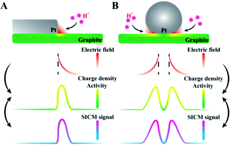 | ||
| Fig. 1 The proposed mechanism for the electric-field enhanced electrochemical activity at the (A) Pt–graphite interface and (B) Pt microparticles at the supporting graphite surface. | ||
Results and discussion
Theoretical derivation of the correlation between the surface charges and the ion concentrations in the diffuse layer
The derivation of the correlation between the charges and the ion concentrations at the electrode surface follows Pauling's principle of electroneutrality, in which the electrons stored on the electrode surface from the external circuit are equal to the total number of excess charges in the diffuse layer.23–25 Surface charge density at the electrode (σ) can be achieved after the integration of the net ion concentration in the diffuse layer following eqn (1).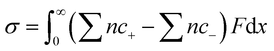 | (1) |
 | ||
| Fig. 2 (A) Theoretical curves of integral charge density within the diffuse layer with the applied voltages of −0.3 and −0.5 V. (B) Theoretical approach curves of the SICM current with different charge densities within the diffuse layer. | ||
Furthermore, the ionic current in SICM is controlled by the ion concentrations in the diffuse layer, which is affected by the charge density at the electrode surface. The theoretical current curves under different charge densities or applied voltages are derived in the ESI.† As demonstrated in Fig. 2B, a large charge density results in a low ion current. To compensate this current drop, the capillary needs to lift up in the constant-current mode. Accordingly, in situ observation of surface charge density in the HER could be realized by SICM imaging. A similar measurement of surface charge using SICM has been achieved by a phase-shift in the current.26
High surface charge at a planar Pt–graphite interface
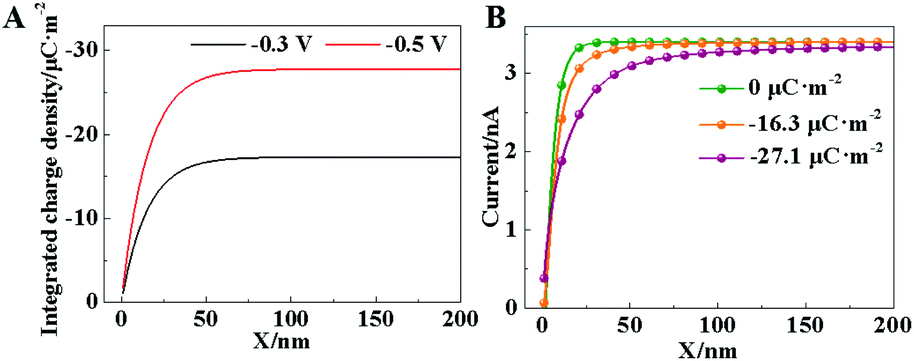
The initial test is performed on a model of the planar Pt–graphite interface by sputtering a layer of Pt onto a part of the graphite surface (Fig. 3A). The peaks of 2θ (39.27 and 45.67°) observed in the X-ray diffraction spectrum (XRD, Fig. S1, ESI†) match well with those from the Pt (111) and Pt (200) surface. The depth at this interface is measured to be ∼327 nm in the hopping mode of SICM (Fig. 3B). It has been reported that the electric field at the interface between two conductive layers (e.g., Pd and Au) is significantly high.23 According to the Laplace equation, the electric field enhancement comes from the difference in the dielectric ability at the interface between two mediums.4 As a result, the electric field line around the interface between the Pt and graphite layer should be more intensive than the surrounding planar surface inducing an enhancement of the electric field strength. Fig. 3C exhibits the simulated distribution of the electric field at this Pt–graphite surface based on the Laplace equation (detailed derivation is in the ESI and more figures are shown in Fig. S2 and S3†).27–30 A maximum electric field of 18![[thin space (1/6-em)]](https://www.rsc.org/images/entities/char_2009.gif) 000 kV cm−1 is obtained at the Pt/graphite interface, as expected (Fig. 3C), which is about 30-fold larger than that at Pt or the graphite surface.
000 kV cm−1 is obtained at the Pt/graphite interface, as expected (Fig. 3C), which is about 30-fold larger than that at Pt or the graphite surface.
 | ||
| Fig. 3 (A) SEM and (B) SICM images of the Pt–graphite interface. (C) The electric field distribution at the Pt–graphite surface. (D) LSV curves from different regions at the Pt–graphite surface. | ||
To investigate the electroreduction activity of this surface in the HER, we used scanning electrochemical cell microscopy (SECCM) to measure the reduction currents in 500 mM H2SO4 (∼1 μm in diameter per cell) at the Pt layer, graphite layer and Pt–graphite interface. Obvious electro-reduction currents are observed at the Pt layer and Pt–graphite interface with a potential less than −0.5 V (Fig. 3D), corresponding to the electrochemical reduction of hydrogen ions. The current density at the Pt–graphite interface is calculated to be ∼230 mA cm−2 at a potential of −0.5 V, which is 3.8-fold larger than that from the Pt surface (∼60 mA cm−2) (Fig. S4A, ESI†). More current observed at the Pt–graphite interface supports a higher electrochemical activity at the interface, as compared with that at the Pt layer. More importantly, the voltage is −0.401 V at a current density of 40 mA cm−2, which is larger than that (−0.475 V) at the Pt layer. Less reduction potential observed at the interface with a higher electric field indicates a lower activation energy for the electrochemical reduction process. Considering that the diffusive flux to the interface should be larger than that to the planar surface, the reduction currents in these two regions are simulated based on the diffusion module using Comsol software. An ∼2 fold increase in the current is obtained at the interface (Fig. S5, ESI†) which indicates that the diffusion is not the only factor to induce the current increase at the interface. Thus, the local electric field should play a role in the up-regulation of electrochemical activity.
The charge at this Pt–graphite surface was further investigated using SICM in 20 mM H2SO4 at voltages of −0.3 and −0.5 V. Before each scanning, the voltages were applied for 10 min to achieve the stable diffuse layer. The schematic setup is shown in Fig. S6 (ESI†) and more details are shown in the ESI.†Fig. 4A shows the distribution of charge density at this surface after the application of −0.3 V, where no electro-reduction occurs at this potential. Similar charge densities (∼19 μC m−2) at the Pt and graphite surfaces are observed. Notably, a charge density as large as 60 μC m−2 is recorded at the Pt–graphite interface, which provides strong evidence for the elevation of the surface charge density in the region with a high electric field.
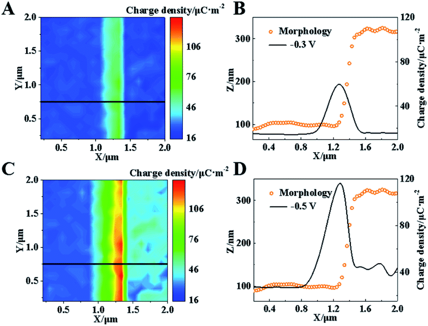 | ||
| Fig. 4 (A) Charge density of the Pt–graphite interface at a voltage of −0.3 V. (B) Morphology and charge density along the black line in (A). (C) Charge density of the Pt–graphite step at a voltage of −0.5 V. (D) Morphology and charge density along the black line in (C). | ||
A continuous decrease in the potential to −0.5 V initiates the electro-reduction process, which induces an elevation of reduction current at the Pt–graphite surface (Fig. S7, ESI†). To minimize the fluctuation of surface charge during the measurement, we apply a voltage at the surface for 10 min before the SICM imaging. A near-constant current guarantees a stable diffuse layer structure during one SICM scanning. When −0.5 V was applied for 240 s to obtain one image, only about 0.29% H+ was consumed according to Faraday's Law. Therefore, the effect resulting from the consumption of H+ by the HER during one imaging can be minimized. The charge densities at the graphite and Pt surfaces are measured to be ∼25 and 40 μC m−2. The higher electro-reduction activity observed in the Pt layer is ascribed to better catalytic activity in the HER from Pt atoms. Importantly, the charge density at the Pt–graphite interface increases to ∼115 μC m−2 (Fig. 4D). The shape of the capillary tip keeps the same (Fig. S8, ESI†), which excludes the possible contribution of additional charges by the deformation of the tip. The analysis of charge density from six randomly selected regions at the interface and planar Pt surface shows that an almost 3-fold increase in the charge density is obtained at the interface under both −0.3 and −0.5 V, compared with that at the planar surface (Fig. S4B, ESI†). These increases are close to the enhancement in the electro-reduction activity (Fig. S4A, ESI†). Coupled with the observation of less reduction potential at the Pt–graphite interface, it is highly suggested that the presence of a locally high electric field induces an increase in surface charge. Under this condition, charge transfer tends to arise in regions with high charge densities, resulting in lower activation energy in the electrochemical reaction and the promoted kinetics of the HER.
The graphite surface without the Pt layer is researched as the control that has the uniform distribution of the electric field at the whole surface. No obvious enhancement in the charges is obtained from this graphite surface (Fig. S9, ESI†). This result confirms that the enhancement in the electric field could only arise at the interface between two mediums with different electric features.
To further support this proposed electrochemical mechanism, a planar Pt/TiO2 interface is fabricated, where the conductivity of TiO2 is poor without the illumination (Fig. S10A, ESI†). The preparation process is shown in the experimental section. After the imaging of the planar Pt/TiO2 interface using SICM, a potential of −0.5 V is applied and the SICM image is recorded. A high charge density is observed at the interface of Pt and TiO2 (Fig. S10B and C, ESI†). The observation of a similar increase in the charge density at a conductive/non-conductive interface (Fig. S10D, ESI†) shows that the electric field enhancement is present at the interface between two mediums, and is not relative to the surface conductivity. It is noted that the enhancement of charge density at the Pt/TiO2 interface is less than that at the Pt/graphite interface, which might be ascribed to the non-charged TiO2 surface under the applied voltage. Thus, the diffuse layer is present on the side of the conductor, not the insulator. Accordingly, although the electric field enhancement occurs at the Pt/TiO2 interface, the increase in the surface charge is less than that at the Pt/graphite interface.
It is known that the marginal electric field enhancement comes from the difference in the dielectric ability at the interface between two mediums (e.g. Pt and graphite), which is the inherent characteristic of the material structure. This enhancement in the electric field induces an increase in the surface charge and electric field strength in the diffuse layer, and thus, accelerates the electrochemical reaction. Simultaneously, a higher concentration of ions is generated in the diffuse layer to keep the complete structure electrically neutral, which could be characterized using SICM imaging. Eventually, the surface charge effect and double layer effect should be in accord with each other, which is ascribed to the marginal electric field enhancement at the interface. The establishment of this new mechanism will not only facilitate the understanding of “active” regions but also provide an alternative strategy to regulate the electrochemical reaction.
High surface charge at a nonplanar Pt–graphite interface
In electrocatalysis, micro-/nanoshaped electrode surfaces have been reported to have high electrochemical activities.31 Therefore, further investigation is conducted using a model of single Pt microparticles on graphite surfaces with sphere-shaped surfaces. The characterization of these Pt microparticles on graphite slides is shown in Fig. S11 (ESI†). Here, two adjacent Pt microparticles (1.8 and 0.6 μm in diameter) are selected as the model, as shown in Fig. 5A. The SICM image in Fig. 5B shows a similar morphology to that observed in the SEM image (Fig. 5A). The electric field at these two Pt particles is simulated based on the Laplace equation, and the results are shown in Fig. 5C. A high electric field is observed in two regions: the cavities between the larger Pt microparticle and the supporting graphite surface (region 1) and the interconnected region between two microparticles (region 2), as labeled in Fig. 5C.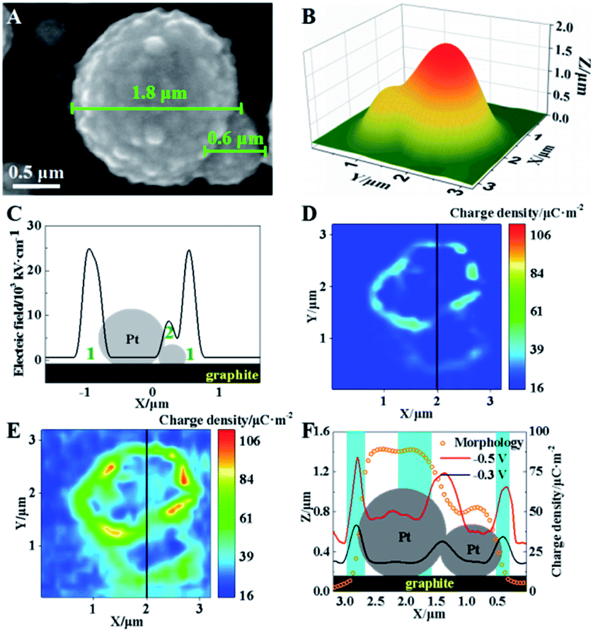 | ||
| Fig. 5 (A) SEM image of two adjacent Pt microparticles. (B) SICM images of these two Pt microparticles. (C) Electric field distribution of Pt particles (the regions of 1 and 2 are labelled). (D and E) Charge density of Pt microparticles at voltages of −0.3 V (D) and −0.5 V (E). (F) Morphology and charge density along the black lines in (D) and (E). | ||
Furthermore, SICM images of surface charge density at Pt microparticles under −0.3 V are exhibited in Fig. 5D. Since the capillary tip could not reach their interface under the equatorial position of the sphere, a higher charge density could be only observed in the diffuse layer surrounding Pt spheres. Although no faradaic reaction occurs under these two voltages, higher charge densities (∼110 μC m−2) are observed in the surrounding cavity (region 1) and the interconnected regions (regions 2). To check the possible change in the morphology of these Pt microparticles, their morphology before and after the application of −0.3 V is characterized using SICM. Almost the same morphology is observed (Fig. S12, ESI†) confirming the stability of the microparticles during the measurement. The spatial coincidence of high charge density and the electric field in the same regions of Pt microparticles supports our proposed mechanism at non-planar surfaces.
When the voltage decreases to −0.5 V, the whole charge density at these two Pt microparticles increases, suggesting the occurrence of electroreduction (Fig. 5E). More specifically, a further increase in the charge density is observed in regions 1 and 2. To demonstrate the clear relationship between the electric field and the charge density, an overlapping plot of the Pt microparticles is shown in Fig. 5F. The simultaneous increase in the electric field and charge density indicates higher electrochemical activity at these cavities and interconnected regions, which is consistent with previous reports.32–36 As a result, our established method provides a new electrochemical characterization with a nanometer resolution to explain the function of “active” regions at the non-planar surface, which is hardly studied by previous electrochemical methods.
Experimental
Chemicals
Commercial highly oriented pyrolytic graphite (graphite) was obtained from Jing Long Te Tan Technology Co. (Beijing, China). Ti foil (100 μm, purity 99.5%) was from Shuangmu Technology Co. (Shanghai, China). The glass capillary (BF100-58-10) was obtained from Sutter Instrument Co. (Novato, CA). Polydimethylsiloxane (PDMS, SYLGARD 184) was purchased from Corning (DOW, US). All chemicals were from Sigma-Aldrich Co., unless indicated otherwise. Ultrapure water with a resistivity of 18.2 MΩ cm−1 was used throughout.Preparation of the Pt–graphite surface and Pt microparticles at graphite
Pt–graphite electrodes were prepared by electrodeposition. Graphite was cut into cubes (20 × 5 × 2 mm3) that were connected with copper wires. Cu wires exposed at the graphite cube surface were covered by PDMS for the insulation. Then, graphite cubes were polished using 1200 and 2000 mesh abrasive paper to obtain a smooth surface. Afterwards, the polished graphites were sonicated in 1 M NaOH solution for 10 min for the cleaning. After rinsing with deionized water three times, they were sonicated again in 1 M HCl solution for 10 min. For the electro-deposition and electrochemical test, the electrode area was controlled at 10 × 5 mm2. The Pt wire and Ag/AgCl electrode were arranged into a disc as the counter and reference electrodes.The electro-deposition was performed in 500 mM H2SO4 solution containing 5 mM H2PtCl4. To obtain a layer of Pt at the graphite surface, cyclic voltammetry (CV) with a potential range from −2.0 to 0 V was conducted for 5 cycles with a scan rate of 200 mV s−1. For the production of Pt microparticles at the graphite surface, only one cycle in the range from −2.2 to 0 V was applied with a scan rate of 10 mV s−1.
Preparation of the Pt–TiO2 interface
Ti foil (100 μm) was used as an anode and another Ti foil served as the cathode. Before anodization, the titanium foils were polished using a mixture solution of HF (40%), HNO3 (65–68%) and deionized water (1:1:2 in volume) for 8 to 10 s. Subsequently, the samples were rinsed thoroughly with deionized water and dried in air. The anodization was processed in ethylene glycol solution with 0.4 wt% H2C2O4 under 60 V at 30 °C to form TiO2. The anodization area was controlled by PDMS. After being washed with ultrapure water and dried in air, the PDMS was removed from the sample. The TiO2 layer was characterized using a scanning electron microscope (SEM, Hitachi S-4800, Japan). The Pt was electro-deposited on the exposed Ti surface using the same protocol as mentioned above.
SICM imaging
The nano-capillary (i.d. ∼ 130 nm, Fig. S8, ESI†) was prepared with glass capillaries (o.d. 1.0 mm, i.d. 0.58 mm) using a P-2000 micropipette puller (Sutter Instrument, pulling parameters: Line 1: Heat 350, Fil 3, Vel 30, Del 220, Pul -; Line 2: Heat 350, Fil 3, Vel 40, Del 180, Pul 120). The whole setup is shown in Fig. S6 (ESI†). SICM (ICnano 2000, Ionscope Co., UK) was used to characterize the morphology and surface charge of Pt–graphite electrodes. The bias between an Ag/AgCl wire in the capillary and the other Ag/AgCl wire in bulk solution was set at 0.2 V to collect the ionic current through the orifice of the nanocapillary. The scanning was performed in 20 mM H2SO4 in the hopping mode. The scan region was set as 2 × 2 μm2 for the Pt–graphite interface and 3.2 × 3.2 μm2 for Pt particles at the graphite surface with a precision of 32 × 32. The threshold of SICM current was set as 1.8% to guarantee the stability of scanning.During the SICM scanning, another voltage of −0.3 or −0.5 V was applied at Pt–graphite electrodes using a CHI 730 to collect the non-faradaic current (−0.3 V) and faradaic current (−0.5 V). An Ag/AgCl wire and a graphite wire were connected with the CHI 730 as the reference and counter electrodes, respectively. Initially, no voltage was applied to the Pt–graphite surface, and the ionic current is collected to image the morphology of the Pt–graphite surface. Then, a voltage (−0.3 or −0.5 V) was applied at the electrode surface, and the ionic current was collected simultaneously. Since the approach curve was associated with the local surface charge, the current collected at a certain distance between the capillary tip and the electrode surface can be used to derive the surface charge. Before each scanning, the voltage was applied at the sample for 10 min to achieve a stable diffuse layer. After each experiment, the samples were scanned using SICM without applied voltage to ensure morphological stability.
SECCM to measure the electrochemical activity in the local electrode region
Micro-capillaries (i.d. ∼ 1 μm) were prepared using the pulling parameters (Line 1: Heat 285, Fil 3, Vel 40, Del 250, Pul 75; Line 2: Heat 285, Fil 4, Vel 40, Del 250, Pul 75). These micro-capillaries were filled with 500 mM H2SO4 to characterize the local electrochemical activity at the Pt–graphite surface. One micro-drop (∼1 μm in diameter) of H2SO4 solution hanged at the tip of the capillary under gravity. The Pt–graphite served as the working electrode while the Ag/AgCl wire inside the capillary served as the reference electrode. Using the micro-manipulator, the capillary moved down with a speed of 5 μm s−1 until a drop of H2SO4 solution was located at the graphite surface, Pt surface or Pt/graphite interface, respectively. A current pulse was observed to confirm the contact of the micro-drop at the Pt–graphite surface. Then, the capillary stopped the movement and the LSV test started. The voltage ranged from 0 to −0.5 V and the scanning rate was 5 mV s−1.Conclusions
In summary, in situ observation of heterogeneous charge distribution at planar and non-planar Pt electrodes in the HER is realized using SICM. By collecting information about the electric field, charge density and electrochemical activity at the electrode, a mechanism in which a locally high electric field induces more charges in these specific regions, resulting in elevated electrochemical activity, is established at the electrode surface. This mechanism will not only facilitate the understanding of “active” regions in electrochemical reactions but also provide a novel regulation of electrochemical reactions using local electric fields. The future quantification of surface charge using SICM is critical for the further establishment of this mechanism, which could be achieved by recently developed quantitative surface conductivity microscopy (QSCM).37,38 Moreover, the further improvement of the temporal resolution of the SICM image is needed to elucidate this electrochemical process dynamically. In addition, the sensitivity of the SICM instrument is being improved in the lab to achieve the imaging of more electrochemical reactions at the electrode to support this proposed mechanism.Conflicts of interest
There are no conflicts to declare.Acknowledgements
We thank the Ministry of Science and Technology of China (2016YFA0201200), the National Natural Science Foundation of China (No. 21874069) and the Open research fund of State Key Laboratory of Bioelectronics, Southeast University for support.Notes and references
- Z. Zhao, C. Chen, Z. Liu, J. Huang, M. Wu, H. Liu, Y. Li and Y. Huang, Adv. Mater., 2019, 31, 1808115 CrossRef PubMed.
- L. Tao, M. Qiao, R. Jin, Y. Li, Z. Xiao, Y. Wang, N. Zhang, C. Xie, Q. He, D. Jiang, G. Yu, Y. Li and S. Wang, Angew. Chem., Int. Ed., 2019, 58, 1019–1024 CrossRef CAS PubMed.
- S. Dou, J. Song, S. Xi, Y. Du, J. Wang, Z.-F. Huang, Z. J. Xu and X. Wang, Angew. Chem., Int. Ed., 2019, 58, 4041–4045 CrossRef CAS PubMed.
- Z. F. Huang, J. Song, Y. Du, S. Dou, L. Sun, W. Chen, K. Yuan, Z. Dai and X. Wang, Carbon Energy, 2019, 1, 77–84 CrossRef.
- Y. Hang, J. H. K. Pfisterer, D. McLaughlin, C. Csoklich, L. Seidl, A. S. Bandarenka and O. Schneider, Small Methods, 2019, 3, 1800387 CrossRef.
- H. Zhang, W. Zhou, T. Chen, B. Y. Guan, Z. Li and X. W. Lou, Energy Environ. Sci., 2018, 11, 1980–1984 RSC.
- J. Chen, Y. Han, X. Kong, X. Deng, H. J. Park, Y. Guo, S. Jin, Z. Qi, Z. Lee, Z. Qiao, R. S. Ruoff and H. Ji, Angew. Chem., Int. Ed., 2016, 55, 13822–13827 CrossRef CAS PubMed.
- H. Liu, Z. Chen, L. Zhou, K. Pei, P. Xu, L. Xin, Q. Zeng, J. Zhang, R. Wu, F. Fang, R. Che and D. Sun, Adv. Energy Mater., 2019, 9, 1901667 CrossRef CAS.
- M. Liu, Y. Pang, B. Zhang, P. De Luna, O. Voznyy, J. Xu, X. Zheng, C. T. Dinh, F. Fan, C. Cao, F. P. G. de Arquer, T. S. Safaei, A. Mepham, A. Klinkova, E. Kumacheva, T. Filleter, D. Sinton, S. O. Kelley and E. H. Sargent, Nature, 2016, 537, 382–386 CrossRef CAS PubMed.
- J. H. K. Pfisterer, Y. Liang, O. Schneider and A. S. Bandarenka, Nature, 2017, 549, 74–77 CrossRef CAS PubMed.
- X. Li, X. Yang, J. Zhang, Y. Huang and B. Liu, ACS Catal., 2019, 9, 2521–2531 CrossRef CAS.
- Y. Zhang, J. M. Lucas, P. Song, B. Beberwyck, Q. Fu, W. Xu and A. P. Alivisatos, Proc. Natl. Acad. Sci. U. S. A., 2015, 112, 8959–8964 CrossRef CAS PubMed.
- X. Liu, C. Zhang, Y. Li, J. W. Niemantsverdriet, J. B. Wagner and T. W. Hansen, ACS Catal., 2017, 7, 4867–4875 CrossRef CAS.
- P. K. Hansma, B. Drake, O. Marti, S. A. C. Gould and C. B. Prater, Science, 1989, 243, 641–643 CrossRef CAS PubMed.
- P. Li, L. Liu, Y. Wang, Y. Yang, C. Zhang and G. Li, Appl. Phys. Lett., 2014, 105, 053113 CrossRef.
- P. Novak, C. Li, A. I. Shevchuk, R. Stepanyan, M. Caldwell, S. Hughes, T. G. Smart, J. Gorelik, V. P. Ostanin, M. J. Lab, G. W. J. Moss, G. I. Frolenkov, D. Klenerman and Y. E. Korchev, Nat. Methods, 2009, 6, 279–281 CrossRef CAS PubMed.
- J. Gorelik, A. I. Shevchuk, G. I. Frolenkov, I. A. Diakonov, M. J. Lab, C. J. Kros, G. P. Richardson, I. Vodyanoy, C. R. W. Edwards, D. Klenerman and Y. E. Korchev, Proc. Natl. Acad. Sci. U. S. A., 2003, 100, 5819–5822 CrossRef CAS PubMed.
- D. Klenerman and Y. Korchev, Nanomedicine, 2006, 1, 107–114 CrossRef CAS PubMed.
- D. Perry, B. P. Nadappuram, D. Momotenko, P. D. Voyias, A. Page, G. Tripathi, B. G. Frenguelli and P. R. Unwin, J. Am. Chem. Soc., 2016, 138, 3152–3160 CrossRef CAS PubMed.
- T. Ji, Z. Liang, X. Zhu, L. Wang, S. Liu and Y. Shao, Chem. Sci., 2011, 2, 1523–1529 RSC.
- M. Kang, D. Perry, C. L. Bentley, G. West, A. Page and P. R. Unwin, ACS Nano, 2017, 11, 9525–9535 CrossRef CAS PubMed.
- K. McKelvey, S. L. Kinnear, D. Perry, D. Momotenko and P. R. Unwin, J. Am. Chem. Soc., 2014, 136, 13735–13744 CrossRef CAS PubMed.
- J. Larminie and A. Dicks, Fuel cell systems explained, Wiley-VCH, Weinheim, 3rd edn, 2018 Search PubMed.
- M. Forghani and S. W. Donne, J. Electrochem. Soc., 2019, 166, A1370–A1379 CrossRef CAS.
- A. C. Forse, C. Merlet, J. M. Griffin and C. P. Grey, J. Am. Chem. Soc., 2016, 138, 5731–5744 CrossRef CAS PubMed.
- D. Perry, R. Al. Botros, D. Momotenko, S. L. Kinnear and P. R. Unwin, ACS Nano, 2015, 9, 7266–7276 CrossRef CAS PubMed.
- J. Jiang, K. Bosnick, M. Maillard and L. Brus, J. Phys. Chem. B, 2003, 107, 9964–9972 CrossRef CAS.
- J. M. Santiago, D. J. Keffer and R. M. Counce, Langmuir, 2006, 22, 5358–5365 CrossRef CAS PubMed.
- L. Jdira, K. Overgaag, J. Gerritsen, D. Vanmaekelbergh, P. Liljeroth and S. Speller, Nano Lett., 2008, 8, 4014–4019 CrossRef CAS PubMed.
- W. J. Chen and H. J. Keh, J. Phys. Chem. B, 2013, 117, 9757–9767 CrossRef CAS PubMed.
- Y. Zhu, L. Peng, Z. Fang, C. Yan, X. Zhang and G. Yu, Adv. Mater., 2018, 30, 1706347 CrossRef PubMed.
- J.-H. Zhong, X. Jin, L. Meng, X. Wang, H.-S. Su, Z.-L. Yang, C. T. Williams and B. Ren, Nat. Nanotechnol., 2017, 12, 132–136 CrossRef CAS PubMed.
- J. Feng, F. Lv, W. Zhang, P. Li, K. Wang, C. Yang, B. Wang, Y. Yang, J. Zhou, F. Lin, G.-C. Wang and S. Guo, Adv. Mater., 2017, 29, 1703798 CrossRef PubMed.
- K. M. Deen, A. Farooq, M. A. Raza and W. Haider, Electrochim. Acta, 2014, 117, 329–335 CrossRef CAS.
- D. Li, X. Li, S. Chen, H. Yang, C. Wang, C. Wu, Y. A. Haleem, S. Duan, J. Lu, B. Ge, P. M. Ajayan, Y. Luo, J. Jiang and L. Song, Nat. Energy, 2019, 4, 512–518 CrossRef.
- Y. Yang, L. Ohnoutek, S. Ajmal, X. Zheng, Y. Feng, K. Li, T. Wang, Y. Deng, Y. Liu, D. Xu, V. K. Valev and L. Zhang, J. Mater. Chem. A, 2019, 7, 11836–11846 RSC.
- L. H. Klausen, T. Fuhs and M. Dong, Nat. Commun., 2016, 7, 12447 CrossRef CAS PubMed.
- T. Fuhs, L. H. Klausen, S. M. Sønderskov, X. Han and M. Dong, Nanoscale, 2018, 10, 4538–4544 RSC.
Footnote |
| † Electronic supplementary information (ESI) available. Theoretical derivation and more SICM images. See DOI: 10.1039/d0sc00223b |
| This journal is © The Royal Society of Chemistry 2020 |