
 Open Access Article
 This Open Access Article is licensed under a Creative Commons Attribution-Non Commercial 3.0 Unported Licence
Dielectric properties of poly-(3-octylthiophene) thin films mixed with oleic acid capped cadmium selenide nanoparticles
Mohsen Elain Hajlaoui a,
Aida Benchaabanebc,
Zied Benhamedc,
Nourdine Mahdhid,
Ahmed A. Al-Tabbakhe and
Fayçal Koukic
a,
Aida Benchaabanebc,
Zied Benhamedc,
Nourdine Mahdhid,
Ahmed A. Al-Tabbakhe and
Fayçal Koukic
aInstitut Supérieur de Technologie Médicale, Université Tunis El-Manar, 1003 Tunis, Tunisia
bLaboratoire Matériaux Avancés et Phénomènes Quantiques, Faculté des Sciences de Tunis El Manar, Université Tunis El-Manar, Campus Universitaire, 2092 Tunis, Tunisia
cEcole d'aviation de Borj El Amri, route Mjez El Beb, 1142 Tunis, Tunisia
dLaboratoire Matériaux, Organisation et Propriétés, Université de Tunis El Manar, Tunis 2092, Tunisia
eDepartment of Physics, College of Science, Al-Nahrain University, Baghdad, Iraq
First published on 22nd December 2020
Abstract
Hybrid heterojunction thin films, based on poly-(3-octylthiophene) (P3OT) polymer and oleic acid (OA)-capped cadmium selenide (CdSe) nanoparticles (NPs) are prepared by a spin-coating method. The structural and morphological properties of the CdSe NPs and of the hybrid thin films are investigated. The results of the dielectric characterization show that conductivity of the hybrid thin films is dependent on frequency and CdSe NP concentration. The Nyquist plots of the impedance characteristics of the layers exhibit circular features irrespective of the NP concentration. The dependence of the dielectric permittivity on frequency and CdSe NP concentration are studied.
Introduction
Bulk heterojunctions (BHJs) of nano-composite materials have received extensive attention from the scientific and technological communities for being potential alternatives to conventional heterojunctions in multiple technological applications.1–5 BHJs are currently used in optoelectronics,6–10 radiation detection and photodetection systems,11,12 dielectrics and photovoltaic devices,13,14 biology and medicine.15–18 In hybrid photovoltaic devices, the polymer and the inorganic components offer additional complementary advantages owing to their low-cost manufacturing processes, flexibility, reproducibility, and versatile functionalities.19–21 In hybrid composite devices, NPs play an important role in improving the optical and electrical properties of the devices.22 Numerous studies have been conducted to investigate the influence, on the charge transfer process, of incorporating nanoparticles into the polymer matrix (i.e. the trapping and de-trapping of charges,23–25 the formation of conductive filament paths, and the charge transfer between the NPs and the organic materials).26–28Furthermore, the efficiency of charge generation may be enhanced by improving the mixing quality of the polymer/nanoparticles thus providing an efficient exciton dissociation at the donor/acceptor interface. Owing to the extended path of the donor/acceptor interface, hybrid composite devices hold the advantage over the traditional multilayer models.29 However, the selection of appropriate inorganic semiconductor NPs for certain applications is still debated in the literature. Zinc selenide (ZnSe), cadmium sulfide (CdS), and other inorganic semiconductors are, nevertheless, suitable candidate materials for optoelectronic applications due to an improved efficiency of the functioning nano-composite devices.30–35
CdSe NPs are known to offer advantageous optoelectronic properties compared with other counterparts.36–38 One way of improving the synthesis of the NPs is by using surface ligands to facilitate charge transfer between the phases.39,40 Several capping agents were used in the synthesis of CdSe NPs such as TOPO, octanethiol, EtPO, TBPO, Pip3PO, and Pyrr3PO.41 Apart from these materials, oleic acid (OA) can be used as a suitable capping agent with CdSe quantum dots (CdSe QD) to largely increase the QD loading and suppress the recombination of the separated charges.42,43
The highest efficiency for such hybrid device was obtained with CdSe NPs and polythiophene.44,45 It is worth mentioning that the morphologies and distribution of the NPs in the polymer matrix represent important parameters influencing the optical and electrical properties, and thus the photovoltaic performances of the device.46
Previously, we have shown that the incorporation of oleic acid-capped CdSe NPs into a conducting host of poly(3-octylthiophene) (P3OT) matrix strongly affects the fluorescence of the hybrid nano-composite system and the photovoltaic performances of the P3OT:wt% OA-capped CdSe bulk heterojunction. In the present work, we study the concentration effect of the OA-capped CdSe NPs on the structural and dielectric properties of the P3OT:OA-capped CdSe composite thin film. We used impedance spectroscopy to characterize the synthesized heterojunction materials. Then, we investigated the charge transport mechanism involved in ac conductivity.
Experimental
The polymer matrix used in this work is poly(3-octylthiophene) (P3OT) having a purity of 99% (procured from Sigma-Aldrich, Germany). The OA-capped CdSe NPs were prepared from a 1![[thin space (1/6-em)]](https://www.rsc.org/images/entities/char_2009.gif) :1 mixture of cadmium acetate and OA in diphenyl-ether following the same method previously reported for preparing OA-capped ZnSe NPs.47 The P3OT was dissolved in chloroform (concentration of 20 g l−1). The mixture was then ultrasonicated for 2 hours at room temperature. The solution was then apportioned into bottles of 10 ml each to which the synthesized OA-capped CdSe NPs were added. Three different nanocomposites were prepared corresponding to the NPs concentrations, these are the pure polymer (0 wt%), the 40 wt% and 80 wt% respectively. The as-prepared solutions were ultrasonicated for 3 hours at room temperature.
:1 mixture of cadmium acetate and OA in diphenyl-ether following the same method previously reported for preparing OA-capped ZnSe NPs.47 The P3OT was dissolved in chloroform (concentration of 20 g l−1). The mixture was then ultrasonicated for 2 hours at room temperature. The solution was then apportioned into bottles of 10 ml each to which the synthesized OA-capped CdSe NPs were added. Three different nanocomposites were prepared corresponding to the NPs concentrations, these are the pure polymer (0 wt%), the 40 wt% and 80 wt% respectively. The as-prepared solutions were ultrasonicated for 3 hours at room temperature.
The substrates were cleaned ultrasonically in distilled water, acetone, ethanol and distilled water sequentially for 15 min. These substrates were dried under a nitrogen gas stream. For the active layer deposition, we used the WS-400BZ-6NPP spin-coater from Laurell at 3000 rpm for 30 s. The last step was depositing a thin film (100 nm thick) of aluminum by using Vinci Technologies TDK-Lambda vacuum evaporator at a background pressure of ≈10−6 Pa. Fig. 1 illustrates the synthesis procedure of the P3OT:wt% OA-capped CdSe hybrid solution.
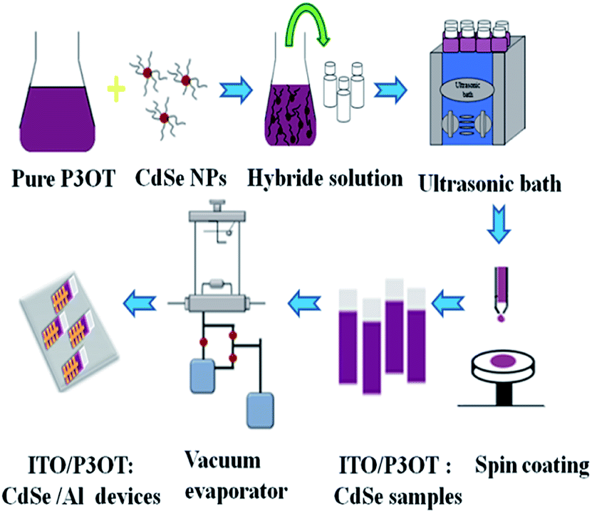 | ||
| Fig. 1 Experimental procedure of the synthesis of P3OT:wt% OA-capped CdSe hybrid solution. | ||
The morphologies and sizes of the OA-capped CdSe NPs were investigated using Tecnai G220 transmission electron microscope (TEM), atomic force microscope (AFM) and a JEOL JSM-6360 scanning electron microscope (SEM).
The structures of the NPs were investigated by X-ray diffraction using the Bruker D4 diffractometer. The Cu-Kα radiation (λ = 1.5418 Å) and Bragg–Brentano setup were used during the measurement of the XRD patterns. The dielectric properties were measured by an Agilent 4294A impedance analyzer in the frequency range 10 to 107 Hz. All the measurements were performed at ambient conditions of pressure and temperature.
Results and discussion
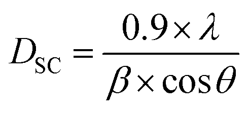
Fig. 2(a) shows the XRD pattern of the OA-capped CdSe NPs in the range 20–80° 2θ. We observed five main broad diffraction peaks, of cubic zinc blend CdSe located at 25.7°, 42.3° 49.8°, 68.2° and 77.8° corresponding to the favorite orientations (111), (220), (311), (133) and (224) respectively. On the other hand, the shoulder peak near the (111) peak of our material may be indexed as (100) and attributed to the presence of uncapped CdSe nanoparticles of hexagonal (Wurtzite) structure.48,49 We determine the average grain size by Scherrer's formula.50
 | (1) |
| β = (βm2 − βi2)1/2 | (2) |
 | ||
| Fig. 2 (a) XRD patterns of the OA-capped CdSe NPs. (b) TEM image of the OA-capped CdSe NPs. | ||
Fig. 2(b) shows the CdSe NPs under TEM. The average diameter of the CdSe NPs is found equal to 8 nm in agreement with that obtained from the XRD measurements.
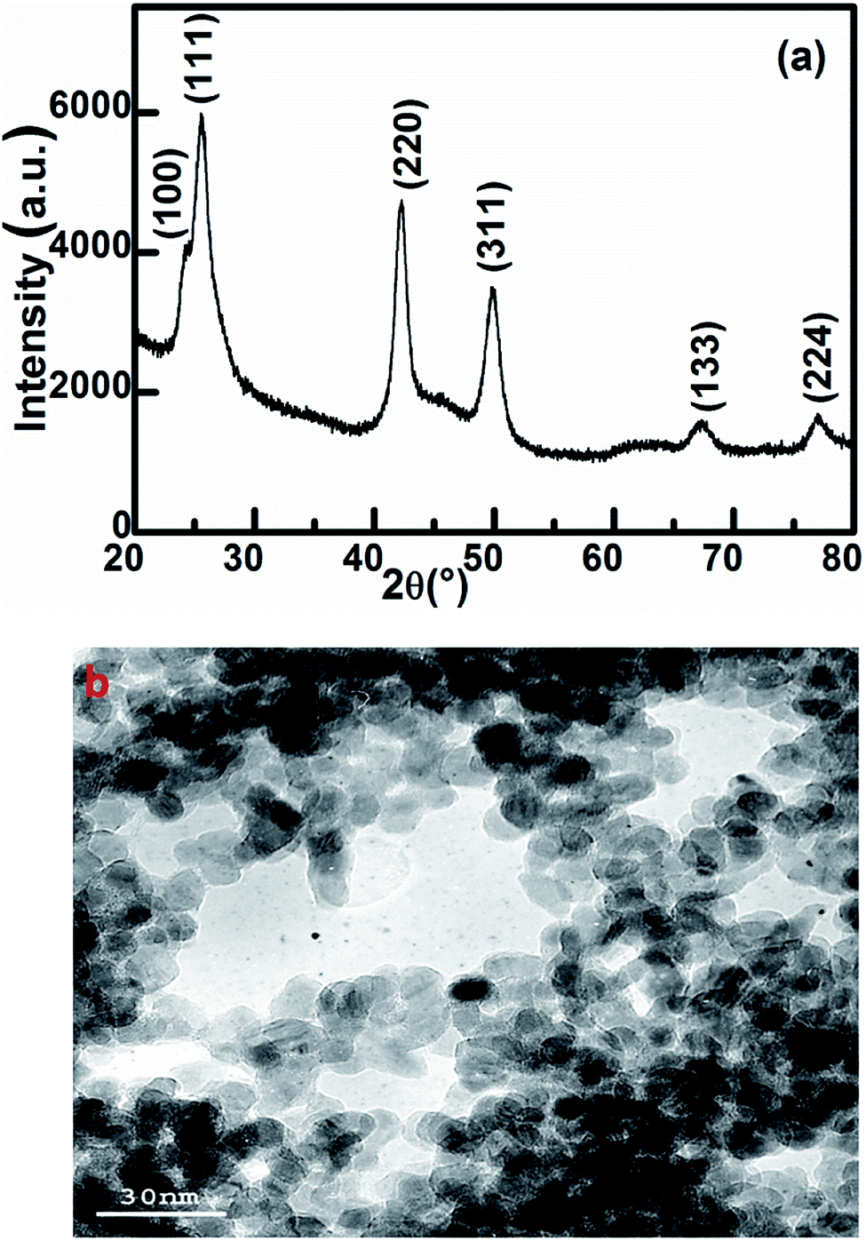
The P3OT:wt% OA-capped CdSe NPs thin films were investigated by SEM as shown in Fig. 3(a–c). The scanning electron micrographs show that the polymeric films are composed of grains stacked on the top of each other. The density of these grains varies from one region to another. The presence of these grains is believed to induce charge accumulation.51 The morphology of the compound polymer is mainly formed by a small grains of lengths varying between 15 nm and 25 nm. This also involves the formation of a hierarchical network of pores as observed under the atomic force microscopy measurements.
 | ||
| Fig. 3 SEM images of P3OT:wt% OA-capped CdSe NPs (a) pure (b) 40% wt (c) 80% hybrid thin films. | ||
The morphology of the deposited P3OT:wt% OA-capped CdSe NPs thin films, obtained using AFM, is shown in Fig. 4(a–c). By comparing the AFM images of the three concentrations prepared in this work, common features were identified. These features are attributed to the preparation condition rather than the NPs concentration in the thin films deposited. The distribution of the NPs obviously changes with the NPs concentration. The nanocomposite films do not cover the substrates totally. This might be attributed to the drying condition of the solution after the deposition process.52,53 The fast drying of the chloroforme solvent is believed to influence the ordering of the P3OT polymer chains resulting in the features observed in the micro-images.54 Similar topography features were observed in other types of polymers.55,56 With regards to the deposition technique used, it is worth mentioning that J. Abad et al. investigated the effect of the deposition technique and found that the spin-coating technique yields a more homogeneous depositions than does the drop-casting technique.57 We have shown that the OA-capped CdSe NPs affect the polymer chain entanglement and maximizes the interface of the P3OT/OA-capped CdSe heterojunction.58 In contrast, the samples containing 40 wt% and 80 wt% of OA-capped CdSe show a decrease in the pore size and height. In the case of the polyvinylcarbazole:ZnSe NPs, increasing the NPs concentration in the polymer matrix was found to affect the topography of the films such that the pores network disappears almost completely at higher concentrations of the NPs. Such effect was attributed to the diffusion of the NPs into the polymer network. These NPs may affect the formation of the polymer percolating network.59–61 As observed in the micrographs, the OA-capped CdSe NPs are well dispersed in the polymer matrix. This results in the augmentation of the polymer/NPs interface leading to an increase in the probability of the exciton dissociation. The average roughness of the films varies from 12.79 nm to 22.27 nm. The roughness varies in an increasing way with concentration.
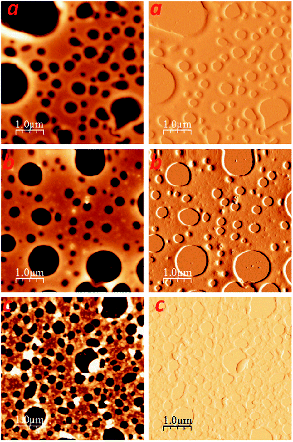 | ||
| Fig. 4 Morphology of the deposited films of P3OT:wt% OA-capped CdSe NPs (a) wt 0% (b) wt 40% and (c) wt 80%. | ||
The increase of roughness enhances the oxygen adsorption process at the crystallites surfaces which act as electron traps. The topography evolution is found directly dependent on the concentration of the OA-capped CdSe NPs (Fig. 4(b and c)). The homogeneous dispersion of the NPs in addition to the pores network plays a major role in facilitating conduction paths of low resistance inducing an inter-chain charge transfer which leads to a gradual increase of conductivity of the P3OT:wt% OA-capped CdSe hybrid thin films.62
The electrical conductivity of the P3OT:wt% OA-capped CdSe thin films in the frequency range 10 to 106 Hz is shown in Fig. 5. Poor conductivity and insignificant dependence of its value on frequency are observed in the frequency range 50 to 104 Hz. At frequencies higher than 104 Hz significant increase of conductivity is observed. In this region, conductivity can be described by the power law:63,64
| σ(ω) = σd + Aωs | (3) |
:NPs interface.67 The complex impedance Z is given by the following equation:68| Z = Z′ − jZ′′ | (4) |
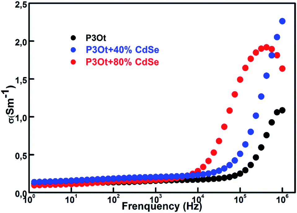 | ||
| Fig. 5 Electrical conductivity of P3OT:wt% OA-capped CdSe hybrid thin film as a function of frequency. | ||
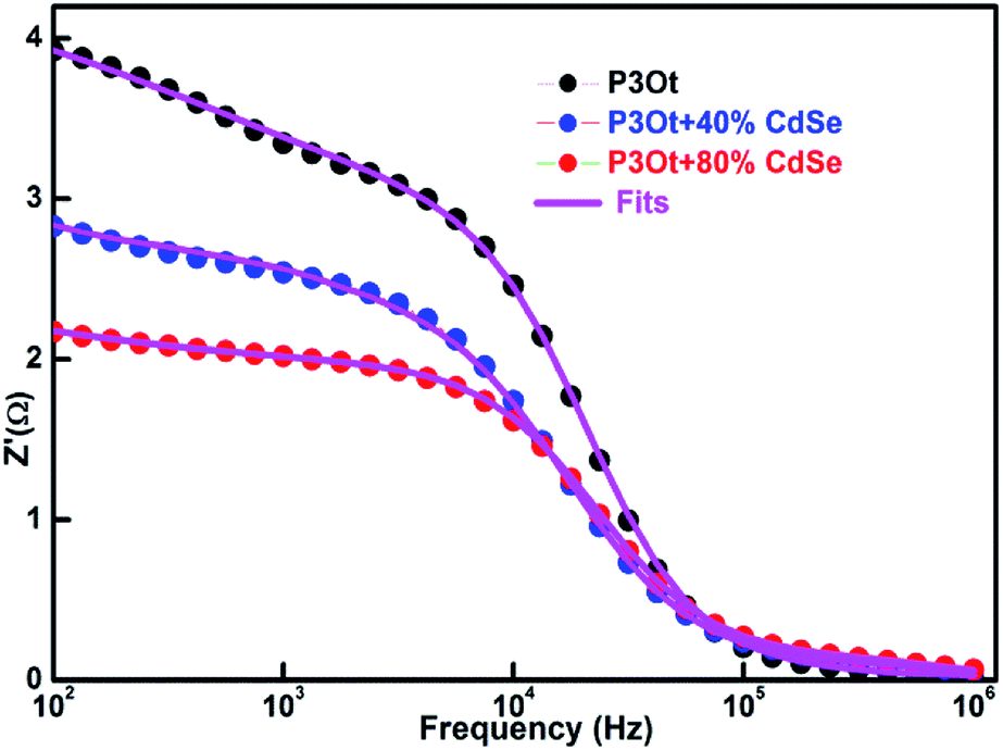 | ||
| Fig. 6 Real component of impedance of P3OT:wt% OA-capped CdSe hybrid thin film as a function of frequency. | ||
The imaginary component of impedance (Z′′) of and the P3OT:wt% OA-capped CdSe hybrid thin films as a function of frequency. The variation of the imaginary part of impedance Z′′ with the frequency at the three concentrations investigated is shown in Fig. 7. A peak-like behavior of the Z′′ at two frequency values is observed for the three polymers:NPs films prepared. The first peak at low frequency value is associated with the effects of the grains boundaries while the second peak at 5 × 10⁴ Hz is attributed to the relaxation of these effects. Z′′ was found to generally decrease with the increase of NPs concentration. The impedance results emphasize that the inclusion and dispersion of the OA-capped CdSe NPs have a profound effect on the impedance characteristics of the samples. This behavior may be associated with two phenomena and affect the impedance spectroscopy results. The first one, is the P3OT/OA-capped CdSe interface contact and the second one is medium and severe clusters formation (i.e. polymer clusters, NPs clusters and complex clusters69) related to the overall decrease of impedance. We would also point out the weak peaks located at the grain resistance region. In the frequency range above 107 Hz the merging of Z′′ may easily be noticed indicating a decrease in the space charge polarization.70
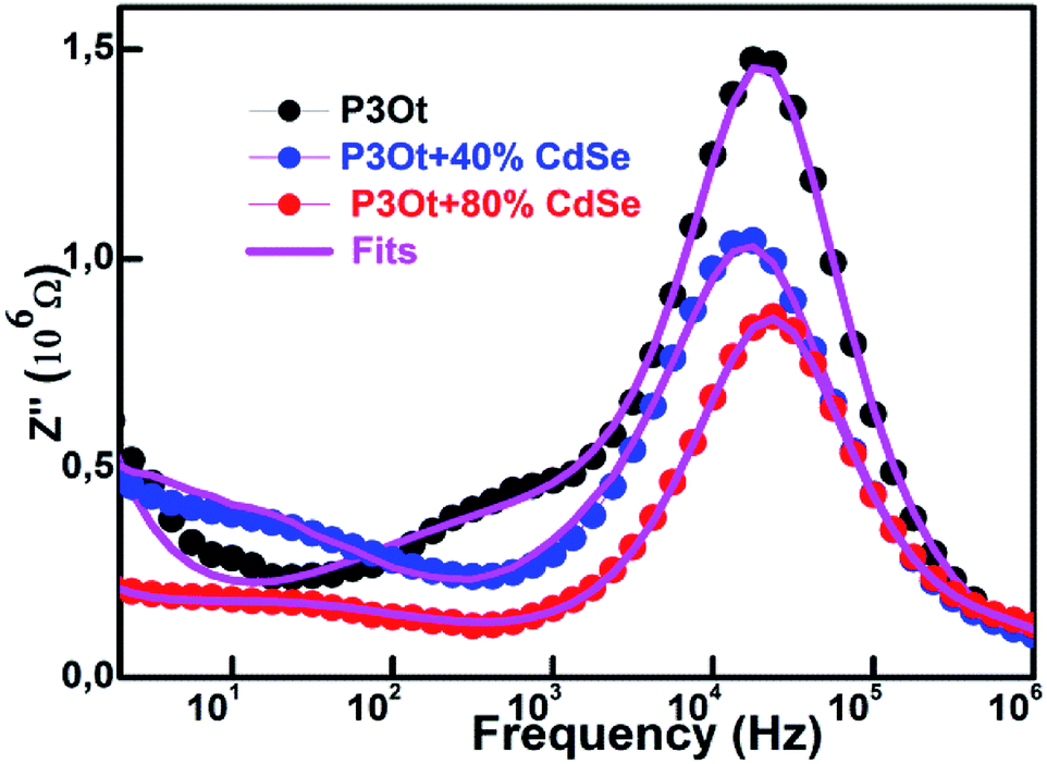 | ||
| Fig. 7 Imaginary component of impedance of P3OT:wt% OA-capped CdSe NPs as a function of frequency. | ||
In order to determine the relaxation time value, we plot the curves of Z′ and Z′′ according to the frequency. The frequency fmax, at which the impedance Z′′ takes its maximum value, corresponds to the inflection point abscissa to the curve of variations of Z′ as a function of the frequency.71
In Fig. 8 we got two inflection points, thus two frequency maxima at 360 Hz and 4.5 × 10⁴ Hz. The relaxation time is calculated from these values using the following equation:72
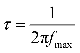 | (5) |
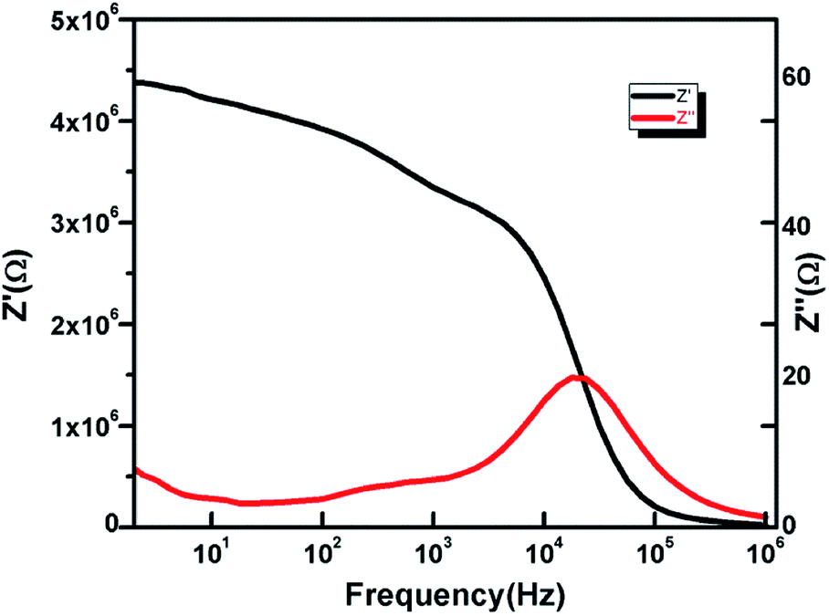 | ||
| Fig. 8 Variation of Z′ and Z′′ of P3OT:wt% OA-capped CdSe NPs hybrid thin film with frequency. | ||
Fig. 9 is the Nyquist plots of the P3OT:wt% OA-capped CdSe NPs hybrid thin films. Two semicircles of different sizes and a linear segment are observed in all the specimens investigated indicating that the key sources of impedance are the same and independent of the OA-capped CdSe NPs. Nevertheless, the semicircle feature which emphasizes the two components/sources of impedance (namely, the double-layer effect at the grain boundaries of the polymer/NPs interface and the charge transfer through the composite material) are found to vary with the concentration of NPs inside the specimen. The decrease of the semicircles sizes with the increase of NPs is attributed to the enhancement of the charge carrier's mobility throughout these charges transferring centers.
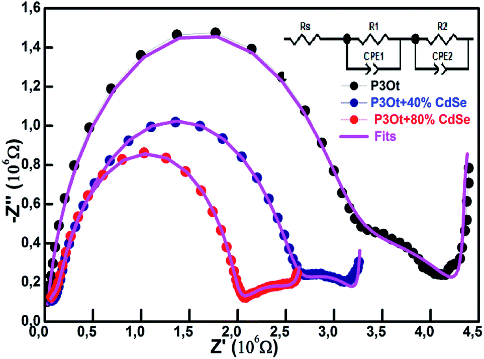 | ||
| Fig. 9 Nyquist diagram of P3OT:wt% OA-capped CdSe NPs hybrid thin film. The inset shows the equivalent circuit. | ||
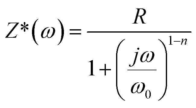
The equivalent circuit is shown in the inset of Fig. 9. Our simulations of the Nyquist plots agree with the measurements and the equivalent circuit was found to reproduce the experimental plots by adjusting the controlling parameters.
The equivalent circuit is composed of two R-CPE (constant phase element) components in parallel with a third resistance Rs has conventionally known Warburg impedance. Warburg impedance is due to lack/depletion of species that otherwise may undergo certain reactions (oxidation/reduction reactions). In the present work, this component is attributed to presence of conductivity zones inside the material associated with the ITO/active layer interface.73,74
The CPE is determined using the following relation:
 | (6) |
 | (7) |
 | (8) |
 | (9) |
The values of constant phase element Ai and resistances Ri for various OA-capped CdSe NPs concentration are listed in Table 1. The data presented a sharp decrease of three resistances when OA-capped CdSe NPs concentration increases. This behavior is explained by different contacts on each side of the pellet and different charge conduction zones. As resistance decreases conductivity increases accordingly.
| Sample | Rs (Ω) | R1 (Ω) | R2 (Ω) |
|---|---|---|---|
| P3OT | 1523 | 2.7488 × 10⁶ | 1.6649 × 10³ |
| P3OT:40% CdSe | 1145 | 2.1144 × 10⁶ | 7.6823 × 10² |
| P3OT:80% CdSe | 940 | 7.7361 × 10⁴ | 1.953 × 10² |
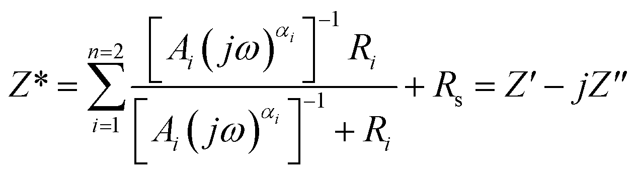
The Frequency dependence of real permittivity ε′ at different OA-capped CdSe NPs concentration is shown in Fig. 10. We noticed that permittivity increases with the concentration of the NPs and this behavior become more significant at low frequency values. At frequencies, less than 104 Hz the real value of permittivity increases with the concentration of NPs indicating that charge carriers are influenced by dipolar and interfacial polarization. This trend, is explained by the Maxwell–Wagner double layer model designed for inhomogeneous structures. At higher frequencies, ionic and electronic polarization contribute to the dielectric constant and they are frequency independent.75,76 Thus, the effect of OA-capped CdSe NPs concentration on dielectric constant is negligible. This could be attributed to the reverse electron motion as the frequency increases leading to reduced polarization.
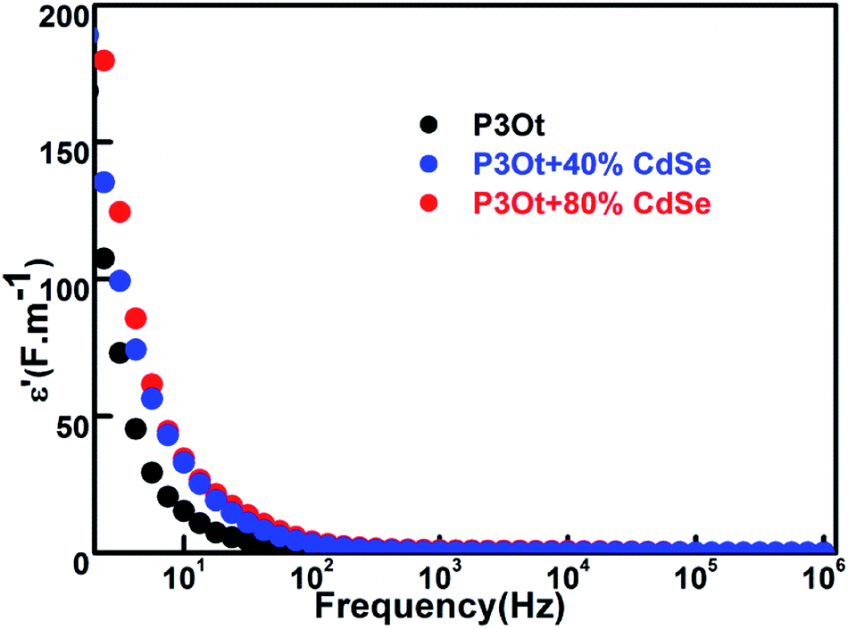 | ||
| Fig. 10 Real part of dielectric constant of P3OT:wt% OA-capped CdSe hybrid thin films as a function of frequency. | ||
Fig. 11 exhibits the variation of imaginary permittivity as a function of frequency at different OA-capped CdSe NPs concentrations. At frequencies less that 103 Hz the imaginary value of permittivity is frequency-on frequency and OA-capped CdSe NPs, contrarily to the strong dependence behavior on frequency seen from the same spectra. Fig. 10 exhibits the variation of imaginary permittivity as a function of frequency at different capon. We note that for frequency (f < 103 Hz) the imaginary permittivity dependence on frequency and OA-capped CdSe NPs concentration. The plots clearly show that curves decreasing as the frequency rises. As the frequency continues to rise, the dielectric constant also continues to lessen. This behavior is explained by the pattern of grain and grain seal or the grain boundaries possess high resistance, so the electrons gather and generate polarization at the boundaries. Thereafter, we notice a rapid decrease of the dielectric constant until independent of frequency.
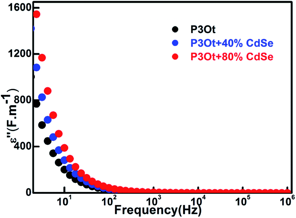 | ||
| Fig. 11 Imaginary part of dielectric constant of P3OT:wt% OA-capped CdSe hybrid thin films as a function of frequency. | ||
Fig. 12 shows the variation of the dielectric loss (tanδ) with frequency at different concentrations of the CdSe NPs. Three regions may be observed. Low-frequency region (50 to 103 Hz) we notice high loss for the different concentration of CdSe NPs then the tanδ decreases as of frequency, followed by a new growth between 5 × 10³ Hz and 5 × 10⁴ Hz. The elevated resistance of grain boundaries at low frequencies results in electrons requiring high energy which justifies the high values of dielectric loss at that region according to Koop's theory.77 The growth in the second region can be explained by the piling up of the electrons at the grain boundaries through a hopping mechanism. There is a reduction of dielectric loss for the higher frequencies and continues to gradually decrease tending towards zero irrespective to OA-capped CdSe NPs concentration. This coalescence is due to the poor energy loss during the exchange of load carriers.
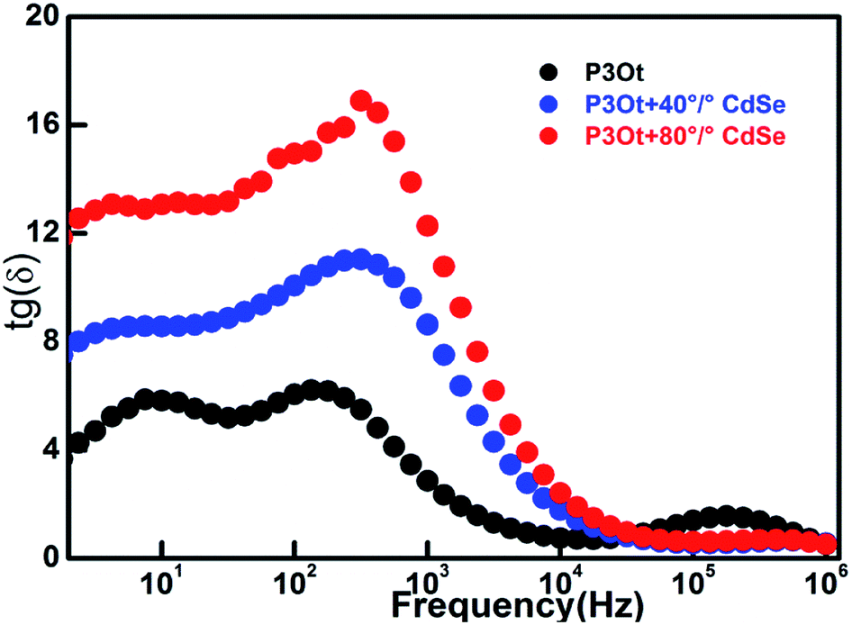 | ||
| Fig. 12 Tangent loss of P3OT:wt% OA-capped CdSe hybrid thin films as a function of frequency. | ||
Enhancing the dielectric parameters of conjugated polymers is an attractive prospect for optoelectronic and microelectronic devices.78,79 The evolution of the dielectric permeability of our samples as a function of frequency covers a large range of frequency (10 to 106), such a similar frequency range is showed by Talfah et al.68 The value of P3OT dielectric constant is very high in comparison with of Aromatic polythiourea (ArPTU) and polyvinylidene fluoride.80 At high frequency, the dipoles cannot follow the oscillation of the applied electric field and the dielectric constant become constant.81 We notice that the contact resistance Rs decreasing when the concentration of NPs increases.67 Generally, there is only one relaxation frequency in polymers, here in our materials, we found two relaxation frequency.82
Conclusion
Thin films of P3OT mixed with oleic acid-capped cadmium selenide NPs were synthesized and deposited successfully by a spin coating method to form a hybrid heterojunction for dielectric applications. The AC electrical conductivity study revealed a strong dependence of conductivity as a function of frequency and concentration of the CdSe NPs. The impedance spectroscopy measurements showed that the charge mobility increases with the increase of the NPs. Two relaxation frequencies were also observed. Agreement between the experimental curves and the simulation data was obtained. We have determined the equivalent circuit for our composite. The circuit is formed by a series of two R-CPE in parallel combination and a third resistance conventionally known as Warburg impedance. Permittivity was found to increase with the concentration of the NPs. The electrical behavior of the dielectric material was associated with the two region effect at the grain boundaries of the polymer/NPs interface and the grain of the composite material.Conflicts of interest
There are no conflicts to declare.References
- M. E. Hajlaoui, N. Hnainia, Z. Gouid, A. Benchaabane, M. A. Sanhoury and R. Chtourou, Optimization of hybrid P3HT:CdSe photovoltaic devices through surface ligand modification, Mater. Sci. Semicond. Process., 2020, 109, 104934 CrossRef CAS.
- E. Salim, S. R. Bobbara, A. Oraby and J. M. Nunzi, Copper oxide nanoparticle doped bulk-heterojunction photovoltaic devices, Synth. Met., 2019, 252, 21–28 CrossRef CAS.
- J. Satra, P. Mondal, U. K. Ghorui and B. Adhikary, In situ systematic metallic gold incorporation to optimize the photon conversion efficiency of AgInS2 thin film semiconductor, Sol. Energy Mater. Sol. Cells, 2019, 195, 24–33 CrossRef CAS.
- W. Ouyang, J. Chen, J. He and X. Fang, Improved Photoelectric Performance of UV Photodetector Based on ZnO Nanoparticle-Decorated BiOCl Nanosheet Arrays onto PDMS Substrate: The Heterojunction and Ti3C2Tx MXene Conduction Layer, Adv. Electron. Mater., 2020, 6, 2000168 CrossRef CAS.
- J. Chen, W. Ouyang, W. Yang, J. H. He and X. Fang, Recent Progress of Heterojunction Ultraviolet Photodetectors: Materials, Integrations, and Applications, Adv. Funct. Mater., 2020, 30, 1909909 CrossRef CAS.
- K. M. A. Saron, M. R. Hashim, M. Ibrahim, M. Yahyaouiad and N. K. Allam, Temperature-dependent transport properties of CVD-fabricated n-GaN nanorods/p-Si heterojunction devices, RSC Adv., 2020, 10, 33526–33533 RSC.
- N. Tessler, V. Medvedev, M. Kazes, S. H. Kan and U. Banin, Efficient near-infrared polymer nanocrystal light-emitting diodes, Science, 2002, 295, 1506–1508 CrossRef.
- A. Benchaabane, Z. Ben Hamed, A. Telfah, M. A. Sanhoury, F. Kouki, K. Zellama and H. Bouchriha, Effect of OA-ZnSe nanoparticles incorporation on the performance of PVK organic photovoltaic cells, Mater. Sci. Semicond. Process., 2017, 64, 115–123 CrossRef CAS.
- A. Benchaabane, J. Belhadi, Z. Ben Hamed, M. Lejeune, A. Lahmar, M. A. Sanhoury, F. Kouki, K. Zellama, A. Zeinert and H. Bouchriha, Effect of CdSe incorporation on the performance of P3OT organic photovoltaic cells, Mater. Sci. Semicond. Process., 2016, 41, 343–349 CrossRef CAS.
- P. Reiss, E. Couderc, J. D. Girolamo and A. Porn, Conjugated polymers/semiconductor nanocrystals hybrid materials preparation, electrical transport properties and applications, Nanoscale, 2011, 3, 446–489 RSC.
- J. Salfi, U. Philipose, C. F. d. Sousa, S. Aouba and H. E. Ruda, Electrical properties of ohmic contacts to ZnSe nanowires and their application to nanowire-based photodetection, Appl. Phys. Lett., 2006, 89, 261112 CrossRef.
- M. Belhaj, C. Dridi, R. Yatskiv and J. Grym, The improvement of UV photodetection based on polymer/ZnO nanorod heterojunctions, Org. Electron., 2020, 77, 105545 CrossRef CAS.
- M. K. Mohanapriya, K. Deshmukh, K. Chidambaram, M. B. Ahamed, K. K. Sadasivuni, D. Ponnamma, M. A. A. AlMaadeed, R. R. Deshmukh and S. K. K. Pasha, Polyvinyl alcohol (PVA)/polystyrene sulfonic acid (PSSA)/carbon black nanocomposite for flexible energy storage device applications, J. Mater. Sci.: Mater. Electron., 2017, 28, 6099–6111 CrossRef CAS.
- X. S. Fang, C. H. Ye, L. D. Zhang and T. Xie, Twinning-Mediated Growth of Al2O3 Nanobelts and Their Enhanced Dielectric Responses, Adv. Mater., 2005, 17, 1661–1665 CrossRef CAS.
- J. H. Son, J. H. Kim, D. H. Park, W. K. Choi, F. Li, J. H. Ham and T. W. Kim, Nonvolatile flexible organic bistable devices fabricated utilizing CdSe/ZnS nanoparticles embedded in a conducting poly-N-vinylcarbazole polymer layer, Nanotechnology, 2008, 19, 055204 CrossRef.
- W. L. Leong, P. S. Lee, S. G. Mhaisklkar, T. P. Chen and A. Dodablapur, Charging phenomena in pentacene- gold nanoparticle memory device, Appl. Phys. Lett., 2007, 90, 042906 CrossRef.
- W. Ouyang, F. Teng and X. Fang, High Performance BiOCl Nanosheets/TiO2 Nanotube Arrays Heterojunction UV Photodetector: The Influences of Self-Induced Inner Electric Fields in the BiOCl Nanosheets, Adv. Funct. Mater., 2018, 28, 1707178 CrossRef.
- F. Li, Z. Qiang, S. Chen, J. Wei, T. Li and D. Zhangd, Synthesis of CdS-loaded (CuC10H26N6)3(PW12O40)2 for enhanced photocatalytic degradation of tetracycline under simulated solar light irradiation, RSC Adv., 2020, 10, 37072–37079 RSC.
- E. J. Bailey and K. I. Winey, Dynamics of Polymer Segments, Polymer Chains, and Nanoparticles in Polymer Nanocomposite Melts: A Review, Prog. Polym. Sci., 2020, 105, 101242 CrossRef CAS.
- C. Zhang, P. L. Yu, Y. Li and J. C. Li, Polymer/TiO2 nanoparticles interfacial effects on resistive switching under mechanical strain, Org. Electron., 2020, 77, 105528 CrossRef CAS.
- X. Zhu, B. Guo, F. Jin, T. Zhai, Y. Wang, G. Li, J. Zhang, Z. Wei, S. Duhm, X. Guo, M. Zhang and Y. Li, Surface modification of ZnO electron transport layers with glycine for efficient inverted non-fullerene polymer solar cells, Org. Electron., 2019, 70, 25–31 CrossRef CAS.
- M. M. Alam, M. Z. B. Mukhlish, A. Tazrin, N. A. Jui, A. M. Asiri, M. M. Rahman, M. A. Islama and M. T. Uddin, A novel highly selective electrochemical chlorobenzene sensor based on ternary oxide RuO2/ZnO/TiO2 nanocomposites, RSC Adv., 2020, 10, 32532–32547 RSC.
- D. I. Son, J. H. Kim, D. H. Park, W. K. Choi, F. Li, J. H. Ham and T. W. Kim, Nonvolatile flexible organic bistable devices fabricated utilizing CdSe/ZnS nanoparticles embedded in a conducting poly-N-vinylcarbazole polymer layer, Nanotechnology, 2008, 19, 055204 CrossRef.
- L. Zhao, L. Hu and X. Fang, Growth and Device Application of CdSe Nanostructures, Adv. Funct. Mater., 2012, 22, 1551–1566 CrossRef CAS.
- W. L. Leong, P. S. Lee, S. G. Mhaisklkar, T. P. Chen and A. Dodablapur, Charging phenomena in pentacene-gold nanoparticle memory device, Appl. Phys. Lett., 2007, 90, 042906 CrossRef.
- B. Cho, T. W. Kim, M. Choe, G. Wang, S. Song and T. Lee, Unipolar nonvolatile memory devices with composites of poly(9-vinylcarbazole) and titanium dioxide nanoparticles, Org. Electron., 2009, 10, 473–477 CrossRef CAS.
- M. Vilkman, K. Solehmainen, A. Laiho, H. G. O. Sandberg and O. Ikkala, Negative differential resistance in polymeric memory devices containing disordered block copolymers with semiconducting block, Org. Electron., 2009, 10, 1478–1482 CrossRef CAS.
- V. S. Reddy, S. Karak, S. K. Rayand and A. Dhar, Carrier transport mechanism in aluminum nanoparticle embedded AlQ3 structures for organic bistable memory devices, Org. Electron., 2009, 10, 138–144 CrossRef CAS.
- A. Benchaabane, Z. B. Hamed, F. Kouki, A. Zeinert and H. Bouchriha, Photogeneration process in bulk heterojunction solar cell based on quaterthiophene and CdS nanoparticles, Appl. Phys. A, 2015, 120, 1149–1157 CrossRef CAS.
- A. Benchaabane, Z. Ben Hamed, A. Telfah, M. A. Sanhoury, F. Kouki, K. Zellama and H. Bouchriha, Effect of OA-ZnSe nanoparticles incorporation on the performance of PVK organic photovoltaic cells, Mater. Sci. Semicond. Process., 2017, 64, 115–123 CrossRef CAS.
- D. S. Ginger and N. C. Greenham, Charge injection and transport in films of CdSe nanocrystals, J. Appl. Phys., 2000, 87, 1361–1368 CrossRef CAS.
- K. F. Jeltsch, M. Schadel and J.-B. Bonekamp, et al., Efficiency enhanced hybrid solar cells using a blend of quantum dots and nanorods, Adv. Funct. Mater., 2012, 22, 397–404 CrossRef CAS.
- K. Kumari, S. Chand, V. D. Vankar and V. Kumar, Enhancement in hole current density on polarization in poly(3-hexylthiophene): cadmium selenide quantum dot nanocomposite thin films, Appl. Phys. Lett., 2009, 94, 213503 CrossRef.
- S. L. Mousavi, F. J. Sheini, M. Sabaeian and R. Yousef, Enhanced solar cell performance of P3HT:PCBM by SnS nanoparticles, Sol. Energy, 2020, 199, 872–884 CrossRef CAS.
- P. Mahajan, A. Singh and S. Arya, Improved performance of solution processed organic solar cells with an additive layer of sol-gel synthesized ZnO/CuO core/shell nanoparticles, J. Alloys Compd., 2020, 814, 152292 CrossRef CAS.
- Y. J. Park, K. S. Lee, G. H. Lim, H. W. Seo, S. W. Kim, M. Kim, Y. Yi, H. S. Lee and D. I. Son, Role of CdSe and CdSe@ZnS quantum dots interlayers conjugated in inverted polymer solar cells, Org. Electron., 2020, 82, 105707 CrossRef CAS.
- W. A. Zoubi, M. P. Kamil, S. Fatimah, N. Nashrah and Y. G. Ko, Recent advances in hybrid organic–inorganic materials with spatial architecture for state-of-the-art applications, Prog. Mater. Sci., 2020, 112, 100663 CrossRef.
- M. Nabil, S. A. Mohamed, K. Easawi, S. S. A. Obayya, S. Negm, H. Talaat and M. K. El-Mansy, Surface modification of CdSe nanocrystals: application to polymer solar cell, Curr. Appl. Phys., 2020, 20, 470–476 CrossRef.
- M. J. Greaney, S. Das, D. H. Webber, S. E. Bradforth and R. L. Brutchey, Improving Open Circuit Potential in Hybrid P3HT:CdSe Bulk Heterojunction Solar Cells via Colloidal tert-Butylthiol Ligand Exchange, J. Am. Chem. Soc., 2012, 6, 4222–4230 CAS.
- Y. Zhou, F. S. Riehle, Y. Yuan, H. F. Schleiermacher, M. Niggeman, G. A. Urban and M. Kruger, Improved efficiency of hybrid solar cells based on non-ligand-exchanged CdSe quantum dots and poly(3-hexylthiophene), Appl. Phys. Lett., 2010, 96, 013304 CrossRef.
- C. Bullen and P. Mulvaney, The Effects of Chemisorption on the Luminescence of CdSe Quantum Dots, Langmuir, 2006, 22, 3007–3013 CrossRef CAS.
- J. Chen, J. L. Song, X. W. Sun, W. Q. Deng, C. Y. Jiang, W. Lei, J. H. Huang and R. S. Liu, An oleic acid-capped CdSe quantum-dot sensitized solar cell, Appl. Phys. Lett., 2009, 94, 153115 CrossRef.
- P. K. Khanna, K. S. Rao, K. R. Patil, V. N. Singh and B. R. Mehta, One-pot synthesis of oleic acid-capped cadmium chalcogenides (CdE:E5 Se,Te) nano-crystals, J. Nanopart. Res., 2010, 12, 101–109 CrossRef CAS.
- N. K. Shrestha, S. J. Yoon, C. Bathula, H. Opoku and Y.-Y. Noh, Hole-induced polymerized interfacial film of polythiophene as co-sensitizer and back-electron injection barrier layer in dye-sensitized TiO2 nanotube array, J. Alloys Compd., 2019, 781, 589–594 CrossRef CAS.
- E. G. M. Morales-Espinoza, A. Ruiu, B. X. Valderrama-García, J. Duhamel and E. Rivera, Design, characterization, optical and photophysical properties of novel thiophene monomers and polymers containing pyrene moieties linked via rigid and flexible spacers, Synth. Met., 2019, 248, 102–109 CrossRef CAS.
- S. Bhattacharyya and A. Patra, Interactions of π-conjugated polymers with inorganic nanocrystals, J. Photochem. Photobiol., C, 2014, 20, 51–70 CrossRef CAS.
- K. S. Rao, N. Singh, K. Gurunathan, R. Marimuthu, N. R. Munirathanam, T. L. Prakash and P. K. Khanna, Nearly mono-disperse quantum dots of ZnSe: synthesis and characterization, Synth. React. Inorg., Met.-Org., Nano-Met. Chem., 2007, 37, 497 CrossRef CAS.
- V. Tzitzios, V. Georgakilas, I. Zafiropoulou, N. Boukos, G. Basina, D. Niarchos and D. Petridis, A General Chemical Route for the Synthesis of Capped Nanocrystalline Materials, J. Nanosci. Nanotechnol., 2007, 8, 1–6 Search PubMed.
- X. Xia, Z. Liu, G. Du, Y. Li and M. Ma, Wurtzite, zinc-blende CdSe based core/shell semiconductor nanocrystals: structure, morphology and photoluminescence, J. Lumin., 2010, 130, 1285–1291 CrossRef CAS.
- Théorie et Technique de la radiocristallographie, ed. A. Guinier and X. Dunod, 3rd edn, 1964, p. 462 Search PubMed.
- L. Shi, Y. Yin, L. C. Zhang, S. Wang, M. Sillanpaa and H. Sun, Design and engineering heterojunctions for the photoelectrochemical monitoring of environmental pollutants: a rev., Appl. Catal., B, 2019, 248, 405–422 CrossRef CAS.
- W. Takashima, S. S. Pandey, T. Endo, M. Rikukawa, N. Tanigaki, Y. Yoshida, K. Yase and K. Kaneto, Photocarrier transports related to the morphology of regioregular poly(3-hexylthiophene) films, Thin Solid Films, 2001, 393, 334–342 CrossRef CAS.
- M. Skompska, Hybrid conjugated polymer/semiconductor photovoltaic cells, Synth. Met., 2010, 160, 1–15 CrossRef CAS.
- L. Xu, H. Zhang, Y. Lu, L. An and T. Shi, The effects of solvent polarity on the crystallization behavior of thin π-conjugated polymer film in solvent mixtures investigated by grazing incident X-ray diffraction, Polymer, 2020, 190, 122259 CrossRef CAS.
- R. Potai, A. Kamphan and R. Traiphol, On the formation of non-emissive and emissive aggregates of regioregular poly(3-octylthiophene) in different local environments, Synth. Met., 2014, 187, 136–144 CrossRef CAS.
- M. E. Nicho, C. H. García-Escobar, M. C. Arenas, P. Altuzar-Coello, R. Cruz-Silva and M. Güizado-Rodríguez, Influence of P3HT concentration on morphological, optical and electrical properties of P3HT/PS and P3HT/PMMA binary blends, Mater. Sci. Eng., B, 2011, 176, 1393–1400 CrossRef CAS.
- J. Abad, B. Pérez-García, A. Urbina, J. Colchero and E. Palacios-Lidón, Layered self-organized structures on poly(3-octylthiophene) thin films studied by scanning probe microscopy, Eur. Polym. J., 2008, 44, 2506–2515 CrossRef CAS.
- A. Benchaabane, Z. Ben Hamed, F. Kouki, A. Zeinert and H. Bouchriha, Photogeneration process in bulk heterojunction solar cell based on quaterthiophene and CdS nanoparticles, Appl. Phys. A, 2015, 120, 1149–1157 CrossRef CAS.
- A. Benchaabane, Z. Ben Hamed, F. Kouki, M. A. Sanhoury, K. Zellama, A. Zeinert and H. Bouchriha, Performances of effective medium model in interpreting optical properties of polyvinylcarbazole: ZnSe nanocomposites, J. Appl. Phys., 2014, 115, 134313 CrossRef.
- M. Taghavimehr, M. Hossein, N. Famili and M. A. Shirsavar, Effect of nanoparticle network formation on electromagnetic properties and cell morphology of microcellular polymer nanocomposite foams, Polym. Test., 2020, 86, 106469 CrossRef CAS.
- A. Cingolani, D. Cuccato, G. Storti and M. Morbidelli, Control of Pore Structure in Polymeric Monoliths Prepared from Colloidal Dispersions, Macromol. Mater. Eng., 2018, 303, 1700417 CrossRef.
- S. Biswas, D.-K. Kim, I.-W. Nam, M. Choi, J.-H. Bae and H. Kim, Highly conductive and thermally stable nanoparticle-conjugated polymer compounds through environmentally friendly in situ synthesis, Prog. Org. Coat., 2020, 142, 105606 CrossRef CAS.
- M. E. Hajlaoui, R. Dhahri, N. Hnainia, A. Benchaabane, E. Dhahri and K. Khirouni, Conductivity and giant permittivity study of Zn0.5Ni0.5Fe2O4 spinel ferrite as a function of frequency and temperature, RSC Adv., 2019, 9, 32395 RSC.
- M. Atif and M. Nadeem, Sol–gel synthesis of nanocrystalline Zn1−xNixFe2O4 ceramics and its structural, magnetic and dielectric properties, J. Sol-Gel Sci. Technol., 2014, 72, 615–626 CrossRef CAS.
- S. Mollah, K. K. Som, K. Bose and B. K. Chaudri, ac conductivity in Bi4Sr3Ca3CuyOx (y = 0 − 5) and Bi4Sr3Ca3−zLizCu4Ox (z = 0.1 − 1.0) semiconducting oxide glasses, J. Appl. Phys., 1993, 74, 931 CrossRef CAS.
- H. Rahmouni, A. Benali, B. Cherif, E. Dhahri, M. Boukhobza, K. Khirouni and M. Sajieddine, Structural and electrical properties of Zn1−xNixFe2O4 ferrite, Appl. Phys. B, 2015, 466–467, 31–37 CAS.
- A. Benchaabane, Z. Ben Hamed, M. A. Sanhoury, F. Kouki, A. Zeinert and H. Bouchriha, Influence of nanocrystal concentration on the performance of hybrid P3HT:TBPO-capped CdSe nanocrystal solar cells, Appl. Phys. A, 2016, 122, 60–70 CrossRef.
- A. Telfah, M. M. Abdul, G. Jafar, I. Jum'h, M. J. A. Ahmad, J. Lambert and R. Hergenröder, Identification of relaxation processes in pure polyethylene oxide (PEO) films by the dielectric permittivity and electric modulus formalisms, Polym. Adv. Technol., 2018, 29, 1974–1987 CrossRef CAS.
- Z. BenHamed, N. Mastour, A. Benchaabane, F. Kouki, M. A. Sanhoury and H. Bouchriha, Franck–Condon analysis of fluorescence quenching in hybrid P3HT:wt% TBPO-capped CdSe quantum dot matrix, J. Lumin., 2016, 170, 30–36 CrossRef.
- E. V. Ramana, S. V. Suryanarayana and T. B. Sankaram, Ac impedance studies of ferro electromagnetic SrBi5−xLaxTi4FeO18 ceramics, Mater. Res. Bull., 2006, 41, 1077–1088 CrossRef CAS.
- M. E. Hajlaoui, R. Dhahri, N. Hnainia, A. Benchaabane, E. Dhahri and K. Khirouni, Dielectric spectroscopy study of the Ni0.2Zn0.8Fe2O4 spinel ferrite as a function of frequency and temperature, Mater. Sci. Eng., B, 2020, 262, 114683 CrossRef CAS.
- K. Ashok, M. B. Suresh and P. Sarah, Electrical properties of Li and Nd doped SrBi4Ti4O15 ceramics, Int. J. Pure Appl. Res. Eng. Technol., 2013, 2, 3299–3307 Search PubMed.
- V. S. Reddy, S. Das, S. K. Ray and A. Dhar, Studies on conduction mechanisms of pentacene based diodes using impedance spectroscopy, J. Phys. D: Appl. Phys., 2007, 40, 7687–7693 CrossRef CAS.
- A. J. Campbell, D. D. C. Bradley and D. G. Lidzey, Space-charge limited conduction with traps in poly(phenylenevinylene) light emitting diodes, J. Appl. Phys., 1997, 82, 6326–6342 CrossRef CAS.
- H. Böttger and U. V. Bryskin, Hopping Conduction in Solids, Verlag Akademie, Berlin, 1985, p. 169 Search PubMed.
- J. C. Dyre and T. B. Schrøder, Universality of ac conduction in disordered solids, Rev. Mod. Phys., 2000, 72, 873–892 CrossRef.
- A. K. Roy, K. Prasad and A. Prasad, Piezoelectric, impedance, electric modulus and Ac conductivity studies on (Bi0.5Na0.5)0.95Ba0.05 TiO3 ceramic, Process. Appl. Ceram., 2013, 7, 81–91 CrossRef CAS.
- G. Horowitz, M. E. Hajlaoui and R. Hajlaoui, Temperature and gate dependence of hole mobility in polycrystalline oligothiophene thin film transistors, J. Appl. Phys., 2000, 87, 4456–4463 CrossRef CAS.
- M. Laajimi, A. Jebnouni, M. Chemli, M. Majdoub and R. Ben Chaabane, Optical, dielectric and oxygen sensing properties of an anthracene and carbazole based π-conjugated Schiff base, Mater. Chem. Phys., 2019, 228, 336–343 CrossRef CAS.
- S. Nasreen and M. Baczkowski, Polymer Dielectric for Capacitor Applications, Kirk-Othmer, Ency. Chem., 2017 Search PubMed.
- P. Chutia and A. Kumar, Dielectric and Conductivity Relaxation in Poly(3,4-ethylenedioxythiophene) Nanotubes, Polym. Eng. Sci., 2016, 448–457 CrossRef CAS.
- S. Das and A. Ghosh, Charge Carrier Relaxation in Different Plasticized PEO/PVDF-HFP Blend Solid Polymer Electrolytes, J. Phys. Chem. B, 2017, 121, 5422 CrossRef CAS.
| This journal is © The Royal Society of Chemistry 2020 |