DOI:
10.1039/D0RA08776A
(Paper)
RSC Adv., 2020,
10, 43847-43852
Comparison of NiOx thin film deposited by spin-coating or thermal evaporation for application as a hole transport layer of perovskite solar cells†
Received
15th October 2020
, Accepted 23rd November 2020
First published on 8th December 2020
Abstract
We compared nickel oxide (NiOx) deposited by thermal evaporation and that deposited by the spin-coating process, for use in the hole transport layers of inverted planar perovskite solar cells (PSCs). Spin-coating deposition for NiOx HTL has been widely used, owing to its simplicity, low cost, and high efficiency. However, the spin-coating process has a technical limit to depositing a large-area uniformly. In contrast, thermal evaporation fabrication has a low price and is able to produce uniform and reproducible thin film. Hence, the chemical states, energy band alignment, surface morphologies, and microstructures of NiOx deposited by spin coating and thermal evaporation were analyzed. The PSC with NiOx HTL deposited by thermal evaporation showed a higher power conversion efficiency of 16.64% with open circuit voltage 1.07 V, short circuit current density of 20.68 mA cm−2, and a fill factor of 75.51% compared to that of PSC with spin-coated NiOx. We confirmed that thermal evaporation can deposit NiOx to give a better performance as a HTL with higher reproducibility than spin-coating.
1 Introduction
Renewable energy is considered a solution for climate change that is causing critical problems such as a sea level rise, and famine. Among the power generation technologies using renewable energy, the photovoltaic cell is a promising technology that converts infinite solar energy into electrical energy. Organic–inorganic halide perovskite solar cells (PSCs) have received attention owing to a remarkable increase in power conversion efficiency (PCE) from 3.8% in 2009, to 25.2% recently.1–6 Organic-inorganic perovskite is represented by the general formula ABX3, where A is an organic/inorganic monovalent cation (methylammonium (CH3NH3+), formamidinium (NH2CH3NH2+), Cs+ or Rb+), B is a divalent metal cation (Pb2+ or Sn2+), and X is a monovalent halide anion (Cl−, Br− or I−).7–9 Perovskite material is suitable to apply to the solar cell, due to its optical and electronic properties. Perovskite has higher absorption coefficient of α > 105 cm−1 and lower exciton binding energy of 30–50 meV than other photovoltaic materials. Because of these properties, the light absorption layer of the PSC is able to generate a lot of electric charge, even at relatively thin thickness. Moreover, the charge in the perovskite layer is easy to move to the charge transport layer, because of the high diffusion carrier mobility of 10–60 cm2 V−1 s−1, long carrier lifetime of ∼100 ns and long-range diffusion lengths (∼1 μm) of the perovskite layer.10–13 The PSC has a structure by which the active perovskite layer is located between the electron transport layer (ETL) and the hole transport layer (HTL), and PSCs are divided into mesoscopic and planar devices, according to the form of the charge transport layer. PSCs are also divided into n–i–p or p–i–n structures, depending on the direction of incident light. If the incident light is through the HTL, it is defined by p–i–n structure. Among these, the p–i–n planar device has been widely studied, due to advantages such as low cost, easy fabrication process, low temperature process, long-term stability and negligible hysteresis effects.14–18
In the interest of improvement in the properties of PSCs, it is important to select the HTL material. From a high-stability point of view, p-type metal oxide with high durability is a suitable candidate for the HTL.15,19 One of the most studied p-type metal oxides for HTL is nickel oxide (NiOx), due to its abundance and chemically stable nature.16 Moreover, NiOx compounds have large bandgap and a deep-lying valance band that cause favorable energy level alignment with the perovskite active layer.14,16,20 NiOx can be synthesized by various kinds of methods,14 such as solution process,21,22 magnetron sputtering process,23 pulsed laser deposition,24 and electron-beam-evaporation.25 Among them, spin-coating, using NiO nanoparticles suspension, has been widely used, owing to its simplicity, and low cost. For example, Liu et al. fabricated NiOx layers using spin-coating for the HTL of PSCs, and obtained a PCE of 15.89%.26 However, the spin-coating process has a technical limit to uniform deposition large-area and upscaling for solution-based processes is difficult to optimize, because it is greatly affected by deposition condition, such as wetting behavior and solvent evaporation.27 Although magnetron sputtering, atomic layer deposition, and laser deposition can obtain uniform and reproducible NiOx thin films, the processing cost is highly increased.28 But the thermal evaporation is a low-cost fabrication process, and it is able to obtain the desired uniformity and reproducibility of thin film.29
In this work, we compared properties, such as structure, energy band level, transmittance, and surface morphology, of NiOx film deposited by thermal evaporation or spin-coating processes on ITO electrode. NiOx deposited by thermal evaporation (thermal-NiOx) and NiOx deposited by spin-coating (spin-NiOx) were applied to PSCs as HTL, and their photovoltaic performances were compared to substitute typical spin-NiOx HTL with thermal-NiOx.
2 Experimental
2.1 Preparation of NiOx thin films
Fig. 1(a) shows a schematic fabrication process by which NiOx is deposited by thermal evaporation and spin-coating processes on the indium tin oxide (ITO) anode. The substrate (2.5 × 2.5 cm2) with pre-coated ITO anode underwent UV/ozone treatment for 30 min before the deposition of thermal-NiOx, and coating of spin-NiOx HTL on top of ITO anode. Thermal-NiOx was deposited 5 nm thick by evaporating NiO granules (>99.9%, 3–12 mm) in the thermal evaporator maintaining a vacuum condition of 1 × 10⁻⁶ torr and deposition rate less than 0.2 Å s−1. We conducted study on the performance of perovskite solar cell according to thickness of thermal-NiOx, as shown in Fig. S1,† and the optimum thickness was set at 5 nm based on the results. Spin-NiOx was deposited that was 30 nm thick by spin-coating NiO nanoparticle solution at 4000 rpm for 40 s, then, it was annealed at 300 °C for 30 min in air. Fig. 1(b) shows a photograph of each sample after deposition.
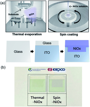 |
| | Fig. 1 (a) Schematic of the fabrication process of the patterned NiOx/ITO anode on glass for the perovskite solar cell. (b) Photograph of NiOx/ITO samples deposited by thermal evaporation or spin-coating. | |
2.2 Characterization of the NiOx HTL
The chemical states of NiOx thin films were investigated by a X-ray photoelectron spectroscopy (K-alpha, Thermoscientific). The energy band alignments of NiOx thin films were confirmed by UV/visible spectroscopy (Lambda 750, PerkinElmer) and ultraviolet photoelectron spectroscopy (NEXSA, Thermoscientific) measurement. The surface morphologies of NiOx thin films and perovskite layers were investigated by field emission scanning electron microscopy (JSM-7600F, JEOL) and atomic force microscope (n-Tracer, NanoFocus) analysis. The microstructures and interface between NiOx thin film and perovskite were analysed by high resolution transmittance electron microscope (JEM-2100F, JEOL). The device performance of solar cells with NiOx HTL was measured using a solar simulator (Oriel Sol3A, Newport) with AM 1.5 G irradiation.
2.3 Fabrication and evaluation of PSCs with NiOx HTL
To evaluate the performance of NiOx as HTL of PSCs, p–i–n PSCs was fabricated. Immediately before perovskite deposition, thermal-NiOx was annealed continuously annealed from room temperature to 330 °C and annealed for 1 min after reaching 330 °C. Because, as shown Fig. S2,† thermal-NiOx has poor wettability for perovskite solution. Then, the perovskite layer was deposited on NiOx HTL from a precursor solution prepared by mixing formamidinium iodide (FAI, 1.09 M), cesium iodide (CsI, 0.25 M), methylammonium bromide (MABr, 0.11 M), lead(II) iodide (PbI2, 1.23 M), and lead(II) bromide (PbBr2, 0.22 M) in N,N-dimethylformamide (DMF) and dimethylsulfoxide (DMSO) (8![[thin space (1/6-em)]](https://www.rsc.org/images/entities/char_2009.gif) :2 v/v). The perovskite precursor solution was spin-coated by continuous two-step process at 500 rpm for 5 s, and 5000 rpm for 45 s. The perovskite precursor solution was spin-coated by continuous two-step process at 500 rpm for 5 s, and 5000 rpm for 45 s. During the second coating step, 0.4 mL of anhydrous chlorobenzene was dropped onto the spinning substrate after 15 s, then annealed at 100 for 30 min. After that, C60, SnO2, and Ag layers were sequentially deposited on a perovskite layer by thermal evaporation process. As electron transport layer, C60 was deposited 35 nm with deposition rate of 0.6 Å s−1 and SnO2 was deposited 3.5 nm with rate 0.1 Å s−1. Finally, 120 nm Ag was deposited as electrode on top. All thermal evaporation processes were performed in maintaining a vacuum condition of 1 × 10⁻⁶ torr.
:2 v/v). The perovskite precursor solution was spin-coated by continuous two-step process at 500 rpm for 5 s, and 5000 rpm for 45 s. The perovskite precursor solution was spin-coated by continuous two-step process at 500 rpm for 5 s, and 5000 rpm for 45 s. During the second coating step, 0.4 mL of anhydrous chlorobenzene was dropped onto the spinning substrate after 15 s, then annealed at 100 for 30 min. After that, C60, SnO2, and Ag layers were sequentially deposited on a perovskite layer by thermal evaporation process. As electron transport layer, C60 was deposited 35 nm with deposition rate of 0.6 Å s−1 and SnO2 was deposited 3.5 nm with rate 0.1 Å s−1. Finally, 120 nm Ag was deposited as electrode on top. All thermal evaporation processes were performed in maintaining a vacuum condition of 1 × 10⁻⁶ torr.
3 Results and discussion
3.1 Chemical states of NiOx thin films
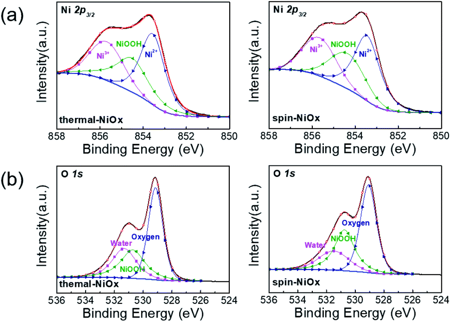
The X-ray photoelectron spectroscopy (XPS) measurements were performed to compare the chemical states and stoichiometries of thermal-NiOx and spin-NiOx HTL. Because of its wide bandgap, the stoichiometric form of NiO is an insulator with a very low intrinsic conductivity of 10−13 cm−1 at room temperature.30,31 But, NiO is a metal-deficient p-type semiconductor, so Ni vacancies are present at the cation lattice site. Due to Ni vacancies, some Ni2+ ions have to be converted to Ni3+ ions in order to maintain the electrical neutrality in the structure, and the created Ni3+ ions take charge of conduction in NiO.32–36 The creation of Ni3+ from Ni2+ can be expressed according to the following reaction:36| |
 | (1) |
where, two Ni2+ ions (NiNix) react with oxygen gas, then create two Ni3+ ions  and ionized nickel vacancy
  The created nickel vacancy and Ni3+ ions in the NiO crystal serve as hole acceptors.36 Fig. 2 shows the XPS spectra of Ni 2p and O 1s. In the Ni 2p3/2 XPS spectra of both thermal-NiOx and spin-NiOx, three peaks are observed, which are located at binding energies of 853.5 eV, 854.5 eV and 855.8 eV. These peaks correspond to the Ni2+, nickel-oxyhydroxide (NiOOH), and Ni3+, respectively. The reason for the NiOOH peak being observed at 854.5 eV, is that the surfaces of both of the samples were hydroxylated, due to atmospheric exposure. The integrated peak area ratio of Ni3+/Ni2+ in the NiOx films calculated from XPS data was equal to 0.69 for both the thermal-NiOx and spin-NiOx. In the oxygen O 1s spectra, the peaks located at 529.1 eV, 530.8 eV and 531.5 eV correspond to oxygen, NiOOH, and water, respectively. The peak area corresponding to the NiOOH of spin-NiOx is larger than that of thermal-NiOx, because the solution process is exposed to more moisture and air than the vacuum process. This result is consistent with the tendency that spin-NiOx has better wettability for perovskite solution, shown in Fig. S2.† But when NiOOH is formed on the surface of a NiOx thin film, the stability and conductivity may be decreased: therefore, it is necessary to control NiOOH on the surface of NiOx thin film.37,38 XPS analysis results indicate that stability and conduction properties of thermal-NiOx are better than spin-NiOx, because the intergrated peak area ratios of Ni3+/Ni2+ of both samples are the same, but spin-NiOx contain more amount of NiOOH.
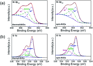 |
| | Fig. 2 XPS spectrum of (a) Ni 2p peaks and (b) O 1s peaks of the NiOx thin film by thermal evaporation and spin coating. | |
3.2 Energy band alignment of NiOx thin films for HTL
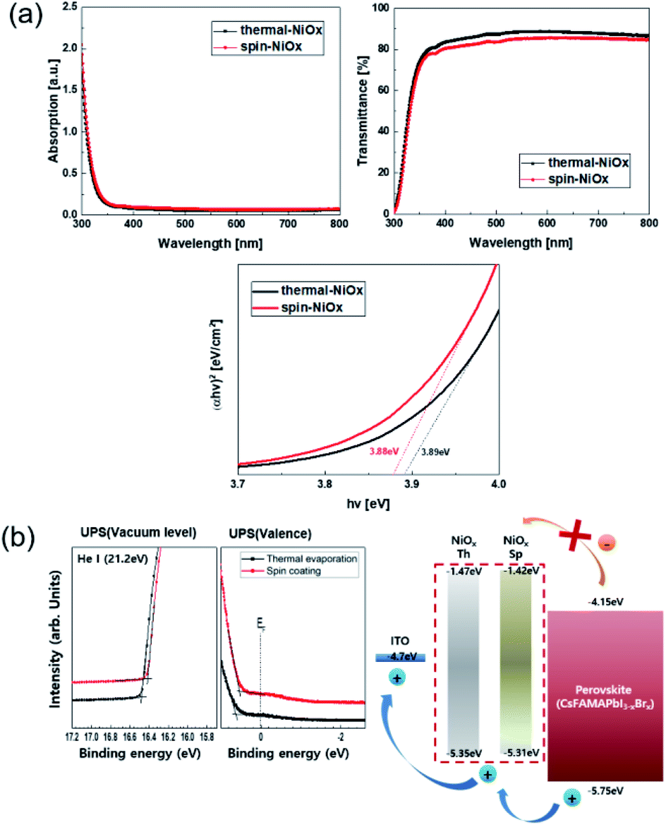
Fig. 3(a) shows the absorbance and transmittance of NiOx thin films that were measured by UV/Vis spectroscopy. The transmittance of thermal-NiOx was slightly higher than that of spin-NiOx, because the thickness of thermal-NiOx is thinner than that of spin-NiOx. The optical energy band gap is calculated using the equation shown below:| | |
αhν = A(hν − Egap)1/2
| (2) |
where α, hν, Egap and A are the absorption coefficient, incident photon energy, optical energy band gap, and constant, respectively.
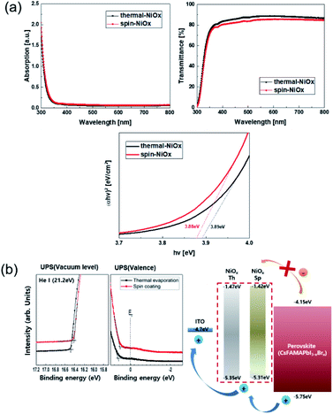 |
| | Fig. 3 (a) Absorbance and transmittance of thermal-NiOx and spin-NiOx thin film deposited on the glass. And optical energy bandgap of thermal-NiOx and spin-NiOx. (b) UPS (He I) spectra and schematic illustration of energy band levels of NiOx with different coating processes. | |
The calculated energy band gap values of thermal-NiOx and spin-NiOx are 3.88 eV and 3.89 eV respectively, and the values are very similar. The ultraviolet photoelectron spectroscopy (UPS) measurement was conducted to analyze the properties of the energy band of NiOx as shown Fig. 3(b). Although there was no noticeable difference in the highest occupied molecular orbital (HOMO), thermal-NiOx showed a slightly lower HOMO than spin-NiOx. Since Voc increases when HTL with deeper HOMO levels are applied to PSCs,10,39–41 it is anticipated that the perovskite device with thermal-NiOx applied has a slightly higher Voc.
3.3 Surface morphologies and microstructures
The surface morphologies of NiOx thin film and perovskite layer were investigated by scanning electron microscopy (SEM) and atomic force microscope (AFM). Fig. 4(a) shows that compared to the surface morphology of spin-NiOx, thermal-NiOx is denser, and has smaller grain size. The grain size of thermal-NiOx is about 25 nm, but the spin-NiOx is approximately 50 nm, twice the size of thermal-NiOx. However, the perovskite layer, coated on the NiOx thin films deposited by different processes, shows a similar surface morphology regardless of the NiOx deposition process, and the grain size is about 200–250 nm. Fig. 4(b) shows the surface morphology image measured by AFM. Spin-NiOx has a rougher surface than thermal-NiOx. The root mean square (RMS) and actual surface area value were calculated through the AFM results. The RMS value of spin-NiOx is 3.29 nm, which is about twice that of the thermal-NiOx (RMS 1.74 nm), and spin-NiOx has a large actual surface area in the same project area. The actual surface area of the spin-NiOx was 1.12 μm2 and that of the thermal-NiOx was 1.00 μm2 per project area (1.00 μm2). Therefore, it is estimated that when NiOx is deposited by spin-coating process using nanoparticles, it has a larger contact area with the perovskite layer. The large contact area between the perovskite layer and HTL reduces charge recombination, and contributes to efficient charge carrier transport.42,43 In contrast, NiOOH present in a large surface area may adversely affect hole transport.
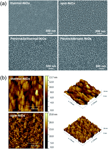 |
| | Fig. 4 Comparision between thermal-NiOx and spin-NiOx morphologies: (a) SEM images of NiOx and perovskite deposited on NiOx, (b) surface image measured by AFM of NiOx deposited using different deposition processes. | |
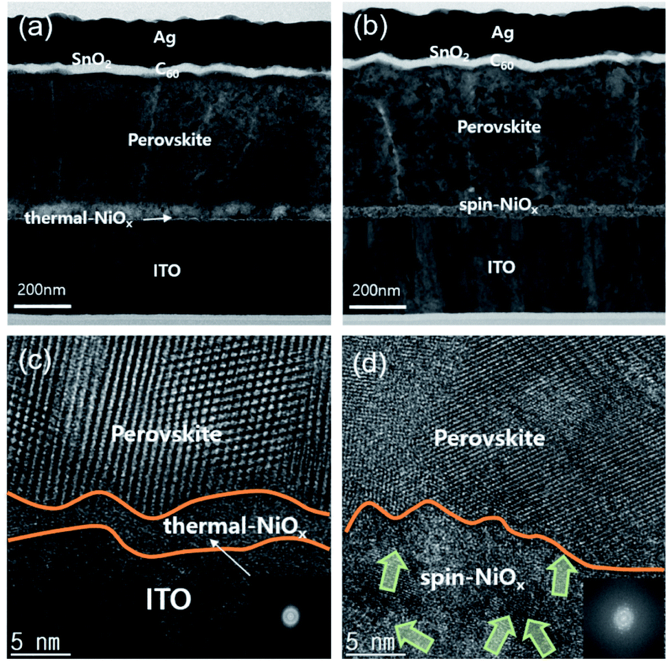
To compare the microstructures and interface of thermal-NiOx and spin-NiOx, high resolution transmission electron microscopy (HR-TEM) was performed and Fig. 5 shows the measured image. Fig. 5(a) and (b) are cross-sectional TEM images of the inverted-planar PSCs with thermal-NiOx or spin-NiOx HTL. All interlayer interfaces of PSCs were well distinguished, and no diffusion at the interface was observed. Fig. 5(c) is enlarged HR-TEM images from the interface between the thermal-NiOx and the perovskite layer. Fig. 5(c) reveals that the crystallization of NiOx has not occurred, since the thickness of thermal-NiOx is very thin (about 5 nm). The diffuse fast Fourier transform (FFT) pattern also confirms the amorphous structure of thermal-NiOx. On the other hand, Fig. 5(d) shows that spin-NiOx consists of nanoparticles grown in random directions and there is a well-defined interface between NiOx and the perovskite layer, without diffusion at the interface. Meanwhile, thermal-NiOx has a smoother interface with perovskite than the spin-NiOx which is consistent with the AFM results.
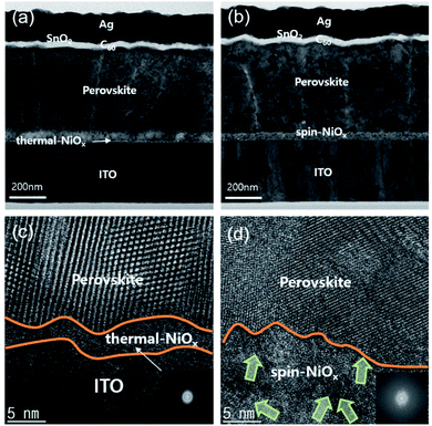 |
| | Fig. 5 Cross-sectional TEM image obtained from perovskite solar cell with (a) the thermal-NiOx HTL, (b) the spin-NiOx HTL. And enlarged HR-TEM images obtained from (c) interface between thermal-NiOx and the perovskite active layer, and interface between ITO and thermal-NiOx, (d) interface between spin-NiOx and perovskite active layer. | |
3.4 Performance of the PSCs contained NiOx HTL
Fig. 6(a) shows the structure of the device that was fabricated to confirm the photoelectric conversion characteristics of the PSC that was applied with NiOx as HTL. And Fig. 6(a) shows the J–V curves of the best performing PSC with each of the thermal-NiOx and spin-NiOx. The best power conversion efficiency (PCE) of PSCs with thermal-NiOx was 16.64% (with Voc = 1.07 V, Jsc = 20.68 mA cm−2 and FF = 75.51%), and that with spin-NiOx was 16.02% (with Voc = 1.02 V, Jsc = 21.14 mA cm−2 and FF = 74.14%). Forward and reverse J–V curves of thermal-NiOx and spin-NiOx were shown in Fig. S3.† PSCs with thermal-NiOx showed little hysteresis, but that with spin-NiOx showed changes in Voc and FF. It is estimated that because spin-NiOx is less stable due to contain more NiOOH than thermal-NiOx, as shown in the XPS data. Fig. 6(b) is a box plot showing the distribution of each parameter obtained from the measurement of numerous J–V curves of the PSCs. The average photovoltaic parameter value of PSCs with thermal-NiOx was PCE = 16.43%, Voc = 1.07 V, Jsc = 20.73 mA cm−2 and FF = 74.00%, whereas that with spin-NiOx was PCE = 15.51%, Voc = 0.99 V, Jsc = 21.80 mA cm−2 and FF = 15.51%. The Voc of PSC using thermal-NiOx was higher than that with spin-NiOx, which is presumed to be because the HOMO level of thermal-NiOx has a deeper value than that of spin-NiOx, as shown in Fig. 3(b). In contrast, Jsc of PSCs using spin-NiOx was higher than that using thermal-NiOx. It is assumed to be because the perovskite layer of PSC with spin-NiOx is exposed to large amount of light than that of PSC with thermal NiOx, as shown in Fig. S4.† Fig. S4† shows the optical transmittance spectra of spin-NiOx/ITO/glass, thermal-NiOx/ITO/glass, and ITO/glass, and the transmittance values are 75.7%, 74.2%, and 77.4% respectively in 300 nm–800 nm. The PCE was higher for PSCs including thermal-NiOx, and all parameters of spin-NiOx have a wider distribution than those of thermal-NiOx. The results show that the thermal evaporation process is advantageous for obtaining a thin film with higher reproducibility than the spin-coating process.
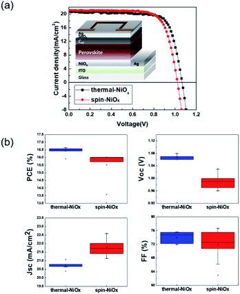 |
| | Fig. 6 (a) Current density–voltage curves and schematics of perovskite solar cell with NiOx for hole transport layer, (b) box chart representation of photovoltaic parameters of perovskite solar cells. | |
4 Conclusions
In summary, we compared a thermal evaporated NiOx and spin-coated NiOx to apply the hole transport layers of PSCs. We evaluated the chemical states, energy band alignments, surface morphologies, and microstructure properties of thermal-NiOx and spin-NiOx thin film. While the chemical states and energy band gaps of thermal-NiOx and spin-NiOx were not significantly different, thermal-NiOx had a slightly deeper HOMO level than did spin-NiOx. But the surface morphologies are different between thermal-NiOx and spin-NiOx with the grain size and RMS of spin-NiOx being about twice as large as that of thermal-NiOx, and the contact area with perovskite layer also being larger. To evaluate the characteristics for HTL, PSCs were fabricated with thermal-NiOx or spin-NiOx and the photovoltaics parameters measured. The PCE of PSCs with thermal-NiOx was higher than that with spin-NiOx and the reproducibility was better. Consequently, we confirmed the performance as HTL of NiOx that was deposited by the thermal evaporation process, and confirmed that the thermal evaporation process is more reproducible than the solution process. Therefore, the thermal evaporation processed NiOx HTL enables large-scale, economic, and reliable fabrication for next generation.
Conflicts of interest
There are no conflicts to declare.
Acknowledgements
This work was supported by the Korea Electric Power Corporation (KEPCO).
References
- Y. Rong, Y. Hu, A. Mei, H. Tan, M. I. Saidaminov, S. I. Seok, M. D. McGehee, E. H. Sargent and H. Han, Science, 2018, 361, 1214 CrossRef CAS
 .
. - H. J. Seok, Y. J. Kang, J. K. Kim, D. H. Kim, S. B. Heo, S. J. Kang and H.-Ki Kim, Sci. Technol. Adv. Mater., 2019, 20, 1118 CrossRef CAS .
- J. H. Lee, D. G. Lee, H. S. Jung, H. H. Lee and H. K. Kim, J. Alloys Compd., 2020, 845, 155531 CrossRef CAS .
- H. J. Seok, A. Ali, J. H. Seo, H. H. Lee, N. E. Jung, Y. J. Yi and H. K. Kim, Sci. Technol. Adv. Mater., 2019, 20, 389 CrossRef CAS .
- M. Zhang, Q. Chen, R. Xue, Y. Zhan, C. Wang, J. Lai, J. Yang, H. Lin, J. Yao, Y. Li, L. Chen and Y. Li, Nat. Commun., 2019, 10, 4593 CrossRef .
- J. G. Kim, J. H. Lee, S. I. Na, H. H. Lee, Y. S. Kim and H. K. Kim, Org. Electron., 2020, 78, 105560 CrossRef CAS .
- N. J. Jeon, J. H. Noh, W. S. Yang, Y. C. Kim, S. C. Ryu, J. W. Seo and S. I. Seok, Nature, 2015, 517, 476 CrossRef CAS .
- W. Xiang and W. Tress, Adv. Mater., 2019, 31, 1902851 CrossRef CAS .
- M. I. Asghar, J. Zhang, H. Wang and P. D. Lund, Renewable Sustainable Energy Rev., 2017, 77, 131 CrossRef CAS .
- Y. Shao, Y. Yuan and J. Huang, Nat. Energy, 2016, 1, 15001 CrossRef CAS .
- A. Dubey, N. Adhikari, S. Mabrouk, F. Wu, K. Chen, S. Yang and Q. Qiao, J. Mater. Chem. A, 2018, 6, 2406 RSC .
- K. P. Bhandari and R. J. Ellingson, A Comprehensive Guide To Solar Energy Systems, Academic Press, Cambridge, 2018, p. 233 Search PubMed .
- Z. Song, S. C. Watthage, A. B. Phillips and M. J. Heben, J. Photonics Energy, 2016, 6, 022001 CrossRef .
- K. D. M. Rao and G. U. Kulkarni, Nanoscale, 2014, 6, 5645 RSC .
- J. K. Kim, D. N. Nguyen, J. H. Lee, S. H. Kang, Y. S. Kim, S. S. Kim and H. K. Kim, J. Alloys Compd., 2020, 818, 152887 CrossRef CAS .
- S. Nair, S. B. Patel and J. V. Gohel, Mater. Today Energy, 2020, 17, 100449 CrossRef .
- R. Wang, M. Mujahid, Y. Duan, Z. K. Wang, J. Xue and Y. Yang, Adv. Funct. Mater., 2019, 29, 1808843 CrossRef CAS .
- L. Meng, J. You, T. F. Guo and Y. Yang, Acc. Chem. Res., 2016, 49, 155 CrossRef CAS .
- L. Calió, S. Kazim, M. Grätzel and S. Ahmad, Angew. Chem., Int. Ed., 2016, 55, 14522 CrossRef .
- J. H. Kim, P. W. Liang, S. T. Williams, N. C. Cho, C. C. Chueh, M. S. Glaz, D. S. Ginger and A. K. Y. Jen, Adv. Mater., 2014, 27, 695 CrossRef .
- U. S. Kwon, B. G. Kim, D. C. Nguyen, J. H. Park, N. Y. Ha, S. J. Kim, S. H. Ko, S. I. Lee, D. H. Lee and H. J. Park, Sci. Rep., 2016, 6, 30759 CrossRef CAS .
- Z. Zhu, Y. Bai, T. Zhang, Z. Liu, X. Long, Z. Wei, Z. Wang, L. Zhang, J. Wang, F. Yan and S. Yang, Angew. Chem., Int. Ed., 2014, 53, 12571 CAS .
- K. C. Wang, P. S. Shen, M. H. Li, S. Chen, M. W. Lin, P. Chen and T. F. Guo, ACS Appl. Mater. Interfaces, 2014, 6, 11851 CrossRef CAS .
- J. H. Park, J. W. Seo, S. M. Park, S. S. Shin, Y. C. Kim, N. J. Jeon, H. W. Shin, T. K. Ahn, J. H. Noh, S. C. Yoon, C. S. Hwang and S. I. Seok, Adv. Mater., 2015, 27, 4013 CrossRef CAS .
- T. Abzieher, S. Moghadamzadeh, F. Schackmar, H. Eggers, F. Sutterlüti, A. Farooq, D. Kojda, K. Habicht, R. l. Schmager, A. Mertens, R. Azmi, L. Klohr, J. A. Schwenzer, M. Hetterich, U. Lemmer, B. S. Richards, M. Powalla and U. W. Paetzold, Adv. Energy Mater., 2019, 9, 1802995 CrossRef .
- Z. Liu, A. Zhu, F. Cai, L. Tao, Y. Zhou, Z. Zhao, Q. Chen, Y. Cheng and H. Zhou, Royal Society of Chemistry, 2017, 5, 6597 CAS .
- S. R. Pae, S. G. Byun, J. K. Kim, M. K. Kim, I. Gereige and B. H. Shin, ACS Appl. Mater. Interfaces, 2018, 10, 534 CrossRef CAS .
- V. Manjunath, S. Bimli, K. H. Parmar, P. M. Shirage and R. S. Devan, Sol. Energy, 2019, 193, 387 CrossRef CAS .
- H. N. Lee and B. J. Song, J Korea Acad Industr Coop Soc, 2011, 12, 2267 CrossRef .
- W. Chen, Y. Wu, Y. Yue, J. Liu, W. Zhang, X. Yang, H. Chen, E. Bi, I. Ashraful, M. Grätzel and L. Han, Science, 2015, 350, 944 CrossRef CAS .
- H. Sato, T. Minami, S. Takata and T. Yamada, Thin Solid Films, 1993, 236, 27 CrossRef CAS .
- D. S. Kim and H. C. Lee, J. Appl. Phys., 2012, 112, 034504 CrossRef .
- N. Kumar, H. B. Lee, S. B. Hwang and J. W. Kang, J. Mater. Chem. A, 2020, 8, 3357 RSC .
- W. Yu, L. Shen, S. Ruan, F. Meng, J. Wang, E. Zhang and W. Chen, Sol. Energy Mater. Sol. Cells, 2012, 98, 212 CrossRef CAS .
- W. Chen, Y. Wu, J. Fan, A. B. Djurišiš, F. Liu, H. W. Tam, A. Ng, C. Surya, W. K. Chan, D. Wang and Z. B. He, Adv. Energy Mater., 2018, 8, 1703519 CrossRef .
- W. L. Jang, Y. M. Lu, W. S. Hwang, T. L. Hsiung and H. P. Wang, Appl. Phys. Lett., 2009, 94, 062103 CrossRef .
- S. Liu, S. Ho, Y. Chen and F. So, Chem. Mater., 2015, 27, 2532 CrossRef CAS .
- S. R. Seo, I. J. Park, M. J. Kim, S. H. Lee, C. D. Bae, H. S. Jung, N. G. Park, J. Y. Kim and H. J. Shin, Nanoscale, 2016, 8, 11403 RSC .
- S. Chen, Y. Hou, H. Chen, M. Richter, F. Guo, S. Kahmann, X. Tang, T. Stubhan, H. Zhang, N. Li, N. Gasparini, C. O. R. Quiroz, L. S. Khanzada, G. J. Matt, A. Osvet and C. J. Brabec, Adv. Energy Mater., 2016, 6, 1600132 CrossRef .
- N. G. Park and W. Tress, Organic-Inorganic Halide Perovskite Photovoltaics, Springer, New-York, 2016 Search PubMed .
- Z. H. Bakr, Q. Wali, A. Fakharuddin, L. Schmidt-Mende, T. M. Brown and R. Jose, Nano Energy, 2017, 34, 271 CrossRef CAS .
- Z. Jin, Y. Guo, S. Yuan, J. S. Zhao, X. M Liang, Y. Qin, J. P. Zhang and X. C. Ai, Royal Society of Chemistry, 2020, 10, 12289 CAS .
- S. Ma, T. Ye, T. Wu, Z. Wang, Z. Wang, S. Ramakrishna, C. Vijila and L. Wei, Sol. Energy Mater. Sol. Cells, 2019, 191, 389 CrossRef CAS .
Footnote |
| † Electronic supplementary information (ESI) available. See DOI: 10.1039/d0ra08776a |
|
| This journal is © The Royal Society of Chemistry 2020 |
Click here to see how this site uses Cookies. View our privacy policy here. 
 Open Access Article
 This Open Access Article is licensed under a
  *a
*a

 and ionized nickel vacancy
  The created nickel vacancy and Ni3+ ions in the NiO crystal serve as hole acceptors.36 Fig. 2 shows the XPS spectra of Ni 2p and O 1s. In the Ni 2p3/2 XPS spectra of both thermal-NiOx and spin-NiOx, three peaks are observed, which are located at binding energies of 853.5 eV, 854.5 eV and 855.8 eV. These peaks correspond to the Ni2+, nickel-oxyhydroxide (NiOOH), and Ni3+, respectively. The reason for the NiOOH peak being observed at 854.5 eV, is that the surfaces of both of the samples were hydroxylated, due to atmospheric exposure. The integrated peak area ratio of Ni3+/Ni2+ in the NiOx films calculated from XPS data was equal to 0.69 for both the thermal-NiOx and spin-NiOx. In the oxygen O 1s spectra, the peaks located at 529.1 eV, 530.8 eV and 531.5 eV correspond to oxygen, NiOOH, and water, respectively. The peak area corresponding to the NiOOH of spin-NiOx is larger than that of thermal-NiOx, because the solution process is exposed to more moisture and air than the vacuum process. This result is consistent with the tendency that spin-NiOx has better wettability for perovskite solution, shown in Fig. S2.† But when NiOOH is formed on the surface of a NiOx thin film, the stability and conductivity may be decreased: therefore, it is necessary to control NiOOH on the surface of NiOx thin film.37,38 XPS analysis results indicate that stability and conduction properties of thermal-NiOx are better than spin-NiOx, because the intergrated peak area ratios of Ni3+/Ni2+ of both samples are the same, but spin-NiOx contain more amount of NiOOH.