
 Open Access Article
 This Open Access Article is licensed under a
 Creative Commons Attribution 3.0 Unported Licence
Strain-enhanced giant Rashba spin splitting in ultrathin KTaO3 films for spin-polarized photocurrents
Ning Wuab,
Xue-Jing Zhang†
ab and
Bang-Gui Liu *ab
*ab
aBeijing National Laboratory for Condensed Matter Physics, Institute of Physics, Chinese Academy of Sciences, Beijing 100190, China. E-mail: bgliu@iphy.ac.cn
bSchool of Physical Sciences, University of Chinese Academy of Sciences, Beijing 100190, China
First published on 15th December 2020
Abstract
Strong Rashba effects at semiconductor surfaces and interfaces have attracted great attention for basic scientific exploration and practical applications. Here, we show through first-principles investigation that applying biaxial stress can cause tunable and giant Rashba effects in ultrathin KTaO3 (KTO) (001) films with the most stable surfaces. When increasing the in-plane compressive strain to −5%, the Rashba spin splitting energy reaches ER = 140 meV, corresponding to the Rashba coupling constant αR = 1.3 eV Å. We investigate its strain-dependent crystal structures, energy bands, and related properties, and thereby elucidate the mechanism for the giant Rashba effects. Further calculations show that the giant Rashba spin splitting can remain or be enhanced when capping layer and/or Si substrate are added, and a SrTiO3 capping can make the Rashba spin splitting energy reach the record 190 meV. Furthermore, it is elucidated that strong circular photogalvanic effect can be achieved for spin-polarized photocurrents in the KTO thin films or related heterostructures, which is promising for future spintronic and optoelectronic applications.
I. Introduction
The Rashba spin–orbit interaction1–3 due to the broken inversion symmetry and the atomic spin–orbit coupling (SOC) can bring about the momentum-dependent spin splitting of the electron states. Rashba effect can play key roles in quantum wells,4 two dimensional (2D) electron gases (2DEG),5 and thin films based on traditional III–V semiconductors.6 After intensive investigations, one can tailor the Rashba coupling by electric field and strain, and design artificial microstructures for various applications. External electric field can be used to modulate the magnitude of Rashba spin splitting in LaAlO3/SrTiO3 (LAO/STO) interface7 and InSe multilayer.8 The Rashba spin splitting can be effectively tuned by varying the interlayer distance in graphene/As–I van der Waals heterostructure9 and adjusting the halogen doping concentration in doped PtSe2 monolayer.10 In addition, it is very interesting to manipulate the Rashba spin–orbit coupling by applying stress, as were done in 2D LaOBiS2,11 binary alloyed hexagonal nanosheets,12 2D heterostructures,13 BiSb monolayer,14 and BiTeI monolayer.15 Large Rashba interaction can be used to realize spin polarization and spin injection by applying electric field16,17 and produce spin-polarized photocurrents through polarized light.18–23Recently, a 2DEG was observed at KTaO3 (KTO) (100) surface24,25 in terms of the angle-resolved photoemission (ARPES) spectrum.24 For another 2DEG at an amorphous-LAO/KTO interface, an experimental analysis of the weak anti-localization effect resulted in a Rashba coupling constant 0.1 eV Å and a 50-fold enhanced Hall mobility of charge carriers.26 Surprisingly, hysteretic magnetoresistance up to 25 K and anomalous Hall effect up to 70 K were observed at an EuO/KTO interface.27 It was shown that LaVO3/KTO heterostructure with strong spin–orbits interactions can be used to produce planar Hall effect, anisotropic magnetoresistance, and 2DEG.28,29 Theoretically, the magnitude of Rashba spin splitting in a KTO surface was studied by applying external electric fields in a symmetric slab model.30 It is highly desirable to investigate the effects of in-plane strain fields on the strength of Rashba spin splitting for KTO surfaces. Actually, strain (stress) is a wonderful approach to manipulate the crystal structures of KTO and thus control their electronic structures and functional properties. Recent studies have demonstrated that the strain can affect the formation and migration of oxygen vacancies in KTO31 and induce electron–hole interchanging of the two opposite surface 2D carrier gases in KTO ultrathin film.32 It has been also shown, experimentally and theoretically, that the KTO (001) 1 × 1 surfaces terminated with KO and TaO2 are most stable compared to others.33,34 Therefore, structurally stable ultrathin KTO (001) films with the two stable surfaces can be manipulated to realize giant Rashba spin effects.
Here, through first-principles calculations and theoretical analyses, we investigate the in-plane strain dependencies of the structural features, intrinsic electrostatic potentials, band edges, carrier concentrations, carrier effective masses, and Rashba parameters of the ultrathin KTO (001) films. We show that their Rashba spin splitting can be controlled by applying biaxial stress, and giant Rashba spin splitting can be obtained by applying compressive biaxial stress, being able to reach 140 meV. In addition, we explore effects of capping layers and/or Si substrate on the giant Rashba spin splitting, and show that a STO capping can make the Rashba spin splitting reach the record 190 meV, as shown in Table 2. Such giant Rashba effects in the ultrathin KTO films can be used to generate spin-polarized photocurrents through circular photogalvanic effect.18–23 More detailed results will be presented in the following.
II. Computational method and parameters
Our first-principles calculation is performed using the projector-augmented wave method within the density-functional theory,35,36 as implemented in the Vienna Ab initio Simulation Package (VASP).37,38 To describe the exchange–correlation energy, we used the general gradient approximation (GGA) with the Perdew–Burke–Ernzerhof for solids (PBEsol) parametrization.39,40 The on-site Coulomb interaction in 5d states of transition-metal ions is corrected by the DFT+U (where U is the Hubbard energy) method.41 The effective value Ueff = 3 eV is employed for Ta 5d states in this work, as it is well established that such a value is appropriate to describe these strongly-correlated states.32 An Monkhorst–Pack k-point grid of 4 × 4 × 1 is used for reciprocal space integration, and the plane wave energy cutoff is set to 500 eV. Our convergence standard requires that the Hellmann–Feynman force on each atom is less than 0.01 eV Å−1 and the absolute total energy difference between two successive consistent loops is smaller than 1 × 10⁻⁵ eV. A fully converged electronic structure is used for further calculation including SOC. Band calculations with SOC are confirmed with larger k-point grid 6 × 6 × 1 in cases of zero and −5% strain values, and the resulting changes are very small. A 20 Å thick vacuum layer is used in the KTO-slab geometry. Additional calculations with vacuum layer of 30 Å and dipole corrections42 are made for confirmation. When a biaxial stress is applied, the in-plane strain is defined as εs = (a − a0)/a0 × 100%, where a0 is the experimental lattice constant of bulk KTO without strain (a0 = 3.989 Å (ref. 43)) and a is the in-plane lattice constant of strained KTO slab. We also optimize cubic KTO bulk by using the above parameters and better convergence standards: k-point grid 15 × 15 × 15, the Hellmann–Feynman force 0.001 eV Å−1, and total energy 1 × 10⁻⁸ eV. This optimization produces the theoretical lattice constant of KTO: aT = 3.996 Å. Because aT is only 0.2% larger than a0, we use the experimental a0 as our reference when defining strain values. Given an in-plane strain value, the out-of-plane lattice and all the internal atomic positions are allowed to relax sufficiently during optimization.III. Results and discussion
A. KTO slab under biaxial stress
We construct a KTO slab model to describe the KTO ultrathin film under different biaxial stresses. The slab consists of m = 12 KTO unit cells along the vertical [001] axis. Fig. 1(a) shows the optimized structure of the KTO slab at the in-plane strain εs = 0% (zero stress). We study the strained KTO slabs with the in-plane strain εs ranging from −5% (compressive) to +8% (tensile). With a given in-plane strain, the system is fully optimized, with the out-of-plane strain being determined by requiring that the out-of-plane stress is zero, and thus we can determine the in-plane stress. Actually, this is a system with biaxial stress. With the condition that the out-of-plane stress is zero, however, the in-plane stress is determined by the in-plane strain. Therefore, for convenience, we shall use the in-plane strain εs to characterize the strained slabs in the following. It is confirmed that the dipole correction has little effect in these results. In Fig. 1(b–m), we plot the representative electronic band structures along M (π,π) → Γ (0,0) → X (0,π) of the optimized KTO slabs for εs = 0%, −1%, −2%, −3%, −4%, −5%, 1%, 2%, 3%, 4%, 5%, and 6%, respectively. Here, SOC is taken into account, and the k vector is in units of 1/a, where a is the calculated lattice constant of the strained KTO slab. When εs is larger than −2%, the KTO slab remains metallic. For the metallic state, there are electron carriers near the Γ point and hole carriers near the M point, and they form a 2DEG at the TaO2-terminated surface and a 2D hole gas (2DHG) at the KO-terminated surface. It should be pointed out that the electron concentration in the 2DEG is equivalent to the hole concentration in the 2DHG.32 There is a critical strain εs = −2%, as shown in Fig. 1(d). From Fig. 1(g, f and e), it is clear that the KTO slab is insulating for εs = −5%, −4%, and −3%. Therefore, there is a strain-driven metal–insulator transition (MIT) at εs = −2%. For the insulating phase, there is an indirect semiconductor gap increasing with |εs + 0.02|, with the conduction band minimum (CBM) being at Γ point and the valence band maximum (VBM) at the M point. | ||
| Fig. 1 (a) Side view of the optimized atomic structure of the KTO ultrathin film (slab) at εs = 0%. (b–m) Band structures of the KTO ultrathin film at different strain values: εs = 0%, −1%, −2%, −3%, −4%, −5%, 1%, 2%, 3%, 4%, 5%, and 6%. The K, Ta, and O atoms are shown by the purple, yellow, and red balls, respectively. The Fermi level Ef is at the zero energy. | ||
To show the stress-driven structural features, we present in Fig. 2 the monolayer-resolved intra-monolayer ionic bucklings (Bi, defined as the maximal cation–anion out-of-plane difference within the monolayer), out-of-plane cation displacements with respect to the centers of the nearest O anions (DKi and DTi), out-of-plane Ta displacements with respect to the centers of the nearest K atoms (DEi, defined only for even i), and inter-monolayer spacings (Si) of the slab under the in-plane strain values between −5% and 6%. It is clear that the atomic positions of the surfaces change substantially with respect to the internal region in the four aspects, and in the internal region the four aspects are made nearly independent of monolayers at strong tensile strains. It is interesting that all the four values monotonically decrease with tensile strain, but increase with compressive strain. When the compressive in-plane strain becomes strong, the bucklings of the surface monolayers are substantially enhanced, and the displacements in the KO monolayers (the TaO2 monolayers) converge to a nearly constant value d1 (d2), with d2 > d1. By combining the buckling and spacing values, it is visible that the two surface single-unit-cells are a little separated from the main body, which is useful to reduce the effect of polarity and stabilize the slab structure. DEi is frequently used in experimental measurement reflecting polarization. It is enhanced by compressive stress and reduced by tensile stress.
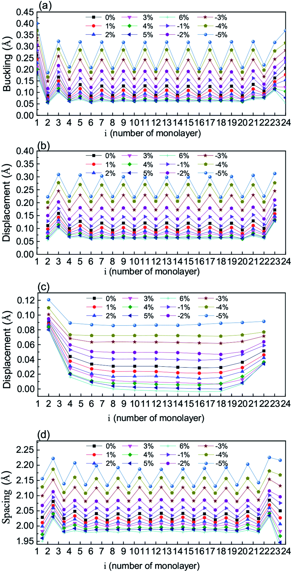 | ||
| Fig. 2 The monolayer-resolved intra-monolayer bucklings (a), displacements of cations (K, Ta) with respect to the nearest O anions (b), displacements of Ta with respect to the nearest K atoms (c), and inter-monolayer spacings (d) of the KTO slab at the different εs values. | ||
Furthermore, we plot in Fig. 3(a) the plane-averaged electrostatic potentials for εs = −5%, −3%, 0, and 4% as representative strain values. It is clear that the maximal (or minimal) value increases from the left to right hand side in the cases of εs = −3%, 0, and 4%, but remains the same for εs = −5%. The internal electric field Eint can be estimated from the slope of the plane-averaged electrostatic potential shown in Fig. 3(a).44 The calculated results as a function of εs are presented in Fig. 3(b). The internal electric field at the unstrained KTO slab is 7.1 × 10⁻² V Å−1, comparable with a previous study.45 It is clear that Eint slowly decreases with tensile strain, and accelerates with compressive strain, nearly reaching zero at εs = −5%. It is expected that the out-of-plane cation displacements with respect to the neighboring O atoms counteract the out-of-plane polarity of the KTO slab, which originates from the oppositely charged (TaO2)+ and (KO)− monolayers. When the compressive strain reaches εs = −5%, corresponding to the in-plane lattice constant 3.789 Å, the potential slope is almost diminished by the increasing polarization due to displacements. The large changes in Eint caused by strong compressive strains will change the energy bands.
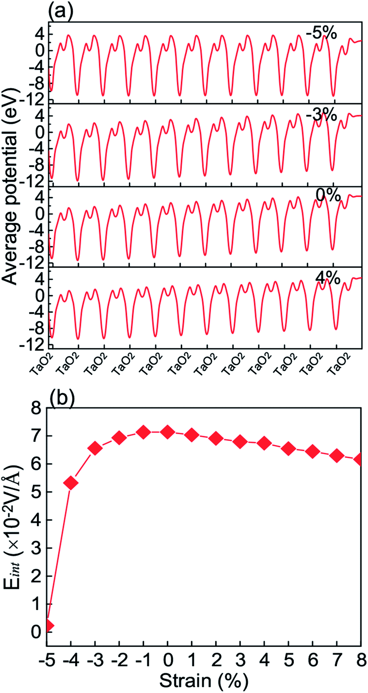 | ||
| Fig. 3 (a) The monolayer-resolved plane-averaged electrostatic potentials of the KTO slab for strain εs = −5%, −3%, 0%, and 4%, respectively. (b) The internal electric field (Eint) as a function of the strain εs. | ||
B. Energy band parameters
To elucidate the band edges and electron concentrations for the strained KTO slab, we present in Fig. 4 the magnified electron band structures of the KTO slab near the Γ point for εs = −4%, 0%, and 5%. In the absence of SOC, the quantum confinement reduces the initial cubic symmetry of the Ta t2g orbitals in the bulk perovskite. The triple degeneracy (excluding spin) of the t2g bands at the Γ point is lifted, splitting the dxy from dxz/dyz. When the inversion symmetry breaking is taken into account, the Ta atomic SOC further splits the dxz/dyz bands into the upper part and the lower one. For the εs = 0% case shown in Fig. 4(b), only the lowest dxy band is partially occupied and the band minimum (at the zone center) lies 0.089 eV below Ef. The corresponding electron concentration of the 2DEG is 2.67 × 1013 cm−2, which is an order of magnitude smaller than 2 × 1014 cm−2 of the 2DEG formed at an experimental KTO surface from the ARPES measurements.24 This difference can be interpreted by the low formation energy for the oxygen vacancies at the KTO surface,24,46 which allows much more electrons in the 2DEG. For the εs = 5% case shown in Fig. 4(c), the minima of the occupied lowest and second lowest dxy states (at the Γ point) are 0.182 and 0.027 eV below Ef, in which the summed electron concentration is 6.98 × 1013 cm−2, larger than that in the unstrained system. For the εs = −4% case shown in Fig. 4(a), the lowest dxy band lies 0.31 eV above the Ef, which means that there are no carriers (without doping), in contrast with those of the εs = 0% and 5% cases.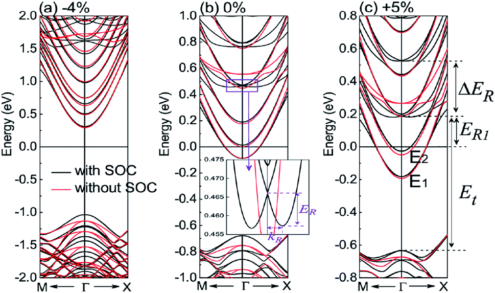 | ||
| Fig. 4 The band structures around Γ point of the KTO slab with (black) and without (red) SOC for εs = −4%, 0%, and 5% are magnified in (a), (b) and (c), respectively. The inset of (b) shows the definition of ER and kR used for estimating the Rashba parameters. The lowest and second lowest dxy bands are labeled by E1 and E2. | ||
It is obvious that there are some Rashba-like spin splitting in the conduction bands of the KTO slab for the εs between −5% and 8%. To further investigate the Rashba effects, we also present in Fig. 4 the magnified electron band structures with SOC of the KTO slab near the Γ point for εs = 0%.
To better describe the properties of the lowest and second lowest dxy conduction bands near the Γ point respectively, defined by E1 and E2 in Fig. 4(c), we investigate and show the band edge positions, electron effective masses, and 2DEG concentrations of the E1 and E2 bands as functions of εs in Fig. 5. In Fig. 5(a), as εs changes from −5% to 4%, the band edge positions of E1 and E2 decrease rapidly with large compressive strain, but they change slowly with tensile strain. As εs varying from 5% to 8%, the band edge positions of E1 and E2 are almost unchanged. It should be noted that the bottom of the conduction band is less affected by the tensile strain, while it is significantly changed by the compressive strain. In detail, the band edge of the E1 band is below Ef for εs ≥ −1%, and that of E2 becomes below Ef for εs ≥ 1%.
 | ||
| Fig. 5 The strain εs dependencies of the energy positions of the E1 and E2 bands (a), the corresponding electron effective masses m* (b), the 2DEG concentration n (c), and the Rashba spin splitting energy ER and k-vector offset kR (d). The E1 and E2 bands are defined in Fig. 4. | ||
In Fig. 5(b), the effective mass (m*) is evaluated from a second-order fit of the band energies using 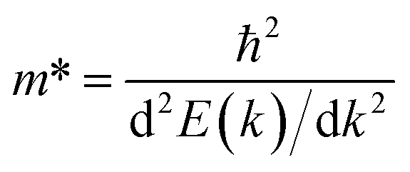 .47 Remarkably, the values of
  for E1 and
  for E2 in the unstrained KTO system are 0.35 and 0.32me (me is the mass of the free electron), respectively, which are both in excellent agreement with 0.30me for the KTO surface 2DEG measured by ARPES.24 When the strain changing from εs = −5% to 8%,
  and
and  increase, with
  being always smaller than
  . Under εs = 8%,
  and
and  reach the maximum values 0.38 and 0.37me, respectively, which are still smaller than ∼0.5 and 0.6me recently determined for a surface 2DEG on STO.48 This suggests that developing high-mobility oxide electronics by KTO is better than by STO.
Fig. 5(c) shows the relationship between εs and the carrier concentrations. For εs ≤ −2%, the E1 and E2 bands are empty and the KTO film is insulating, which is consistent with the critical strain of insulator–metal transition shown in Fig. 1. The carrier concentrations n1 and n2 for the E1 and E2 bands have the maximum values at the εs = 5% and 4%, respectively, and the total 2DEG concentration n of the E1 + E2 bands reaches the maximum values of 7.06 × 1013 cm−2 at εs = 4%. This indicates that the conductivity of the 2DEG formed at the surface can be effectively modulated by the in-plane strain.
In addition, we summarize in Table 1 the energy differences (ER1 and Et) and the spin–orbit splitting energy ΔER between the lowest and the second lowest Rashba doublets, as defined in Fig. 4.
| Strain | ER1 | Et | ΔER | ER | kR |
|---|---|---|---|---|---|
| εs = 5% | 0.188 | 0.822 | 0.339 | 7 | 0.046 |
| εs = 0% | 0.466 | 1.144 | 0.298 | 9 | 0.054 |
| εs = −1% | 0.603 | 1.282 | 0.309 | 20 | 0.096 |
| εs = −2% | 0.810 | 1.516 | 0.309 | 33 | 0.151 |
| εs = −3% | 1.161 | 1.947 | 0.314 | 51 | 0.154 |
| εs = −4% | 1.618 | 2.652 | 0.325 | 90 | 0.24 |
| εs = −5% | 2.228 | 4.136 | 0.093 | 140 | 0.21 |
C. Rashba spin splitting
Since the KTO slab obeys the C4v point group symmetry, the symmetry-allowed linear spin-momentum coupling can be expressed as3 HR = αR(kxσy − kyσx). According to the linear Rashba model, the dispersion due to the Rashba spin splitting can be described by
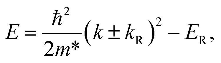 | (1) |
For the KTO slab, the lowest Rashba spin split bands near the Γ point are similar to those defined by eqn (1), and we present ER and kR in Fig. 5(d) for different in-plane strains. The calculated values of ER and kR are summarized in Table 1 for εs = 5%, 0%, −1%, −2%, −3%, −4%, and −5%. In Fig. 5(d), ER and kR increase drastically with the compressive strain increasing, but they both remain almost unchanged for increasing tensile strain. In Table 1, noticeably, ER and kR are 140 (90) meV and 0.21 (0.24) Å−1 for the KTO slab at εs = −5% (−4%). It is clear that compressive in-plane strain can enhance the Rashba spin splitting energy ER. Because Eint is near zero at εs = −5.0%, Eint becomes negative when εs < −5.0%, and consequently the conduction bands are reconstructed, which leads to smaller ER or substantial deformation of the Rashba bands. Actually, this means that the maximal ER is reached at εs = −5%.
To elucidate the mechanism responsible for the giant Rashba spin splitting, we investigate the strain-dependent structural parameters and electrostatic potentials. For the unstrained KTO slab, there is a strong intrinsic electric field e0 due to the out-of-plane alternate alignment of negative KO and positive TaO2 monolayers. When compressive biaxial stress is applied, there are out-of-plane displacements of cations with respect to the neighboring anions driven by the compressive in-plane strain εs and tensile out-of-plane strain, and in addition the ionic displacements cause an out-of-plane electric field ed antiparallel to e0. Our calculated results show that ed increases with εs, reaching the maximum nearly at εs = −5%. Consequently, we can attribute the enhanced giant Rashba spin splitting energy to the strong intrinsic out-of-plane electric field ed due to the large compressive biaxial stress.
For comparison, we summarize the ER, kR, and αR values of some typical Rashba systems in Table 2. For brevity, we can take ER as the key parameter to characterize such Rashba systems. ER can reach 100 meV for BiTeI van der Waals bulk,50 or 190 meV for α-GeTe(111) film.51 In contrast, for perovskite oxides, the previous maximal ER is 15 meV for KTaO3/BaHfO3 interface.52 It is clear that our strategy is very efficient to promote the Rashba spin splitting energy in perovskite oxides because our maximal ER value reaches 140 meV at εs = −5%. Such large Rashba effect is useful to realize strong circular photogalvanic effect.18–23
| System | ER | kR | αR |
|---|---|---|---|
| GaSe/MoSe2 van der Waals HS13 | 31 | 0.13 | 0.49 |
| BiTeI monolayer (εs = 6%)53 | 55.7 | 0.054 | 2.05 |
| BiTeI van der Waals bulk50 | 100 | 0.052 | 3.8 |
| InAlAs/InGaAs interface6 | <1.0 | 0.028 | 0.07 |
| GeTe(111)/InP(111) interface54 | 5.403 | 0.010 | 1.08 |
| α-GeTe(111) film51 | 190.0 | 0.13 | 4.2 |
| BiAlO3 bulk crystal55 | 7.34 | 0.038 | 0.39 |
| LaAlO3/SrTiO3 interface7 | <5.0 | 0.01–0.05 | |
| KTaO3/BaHfO3 interface52 | 15 | 0.3 | |
| KTaO3 film (εs = −5%) | 140 | 0.21 | 1.3 |
| SrTiO3/KTaO3 bilayer (εs = −5%) | 190 | 0.24 | 1.58 |
D. Heterostructures and photogalvanic effect
Recent STM experiment and DFT calculation have already shown that the KTO (001) 1 × 1 surfaces terminated with KO and TaO2 are most stable compared to others.33,34 For more applications, the KTO films could be capped with STO overlayers, and/or should be grown on good substrates. The metallic interfaces can be obtained by generating carriers through experimentally applying gate voltage.56 Furthermore, the STO capping can change the Rashba spin splitting in the bare TaO2-terminated surfaces of KTO films. For the in-plane strains of −3%, −4%, and −5%, our calculations show that the maximal Rashba spin splitting energies are 25, 95, and 190 meV, respectively, and the corresponding k vector offsets are 0.12, 0.19, and 0.24 Å−1. It is a surprise that the STO capping can make the Rashba spin splitting enhanced to 190 meV at strain of −5%! We also study STO/KTO/Si trilayer to simulate capped KTO films on Si substrate. For STO/KTO/Si trilayer, the lattice mismatch is 3.6% for STO/KTO on Si substrate, and then εs is −3.6% and the Rashba spin splitting energy is 51 meV, with the k vector offset being 0.16 Å−1. It is clear that the Rashba effects are still very strong after capping layers and/or substrates are added.Because of the giant Rashba spin splitting, the KTO ultrathin films can be used for achieving circular photogalvanic effect (CPGE) to generate spin-polarized photocurrents.18–23 For the right-handed (left-handed) circularly polarized light, its photon has the angular momentum of +1 (−1), labeled by σ+ (σ−), and the selection rule for necessary transitions is that the allowed z-component change of the total angular momentum is ΔJm = +1 (−1). The valence band edge, originating from the J = 3/2 states, has Jm = ±3/2, and the conduction band edge, from the dxy states of lm = 2 and −2, consists of Jm = ±3/2 and ±5/2 states. Because the dyz/dxz bands have lm = 1 and −1, the Rashba split bands consist of Jm = ±3/2 and ±1/2 states. Therefore, for achieving the CPGE, the electrons can transit from the valence band top (with photon energy Et) or the filled conduction band edge  to the dyz/dxz-based bands with giant Rashba spin splitting as the final states, as shown in Fig. 6(a). When the electron concentration is small,
  is a little lower than ER1.
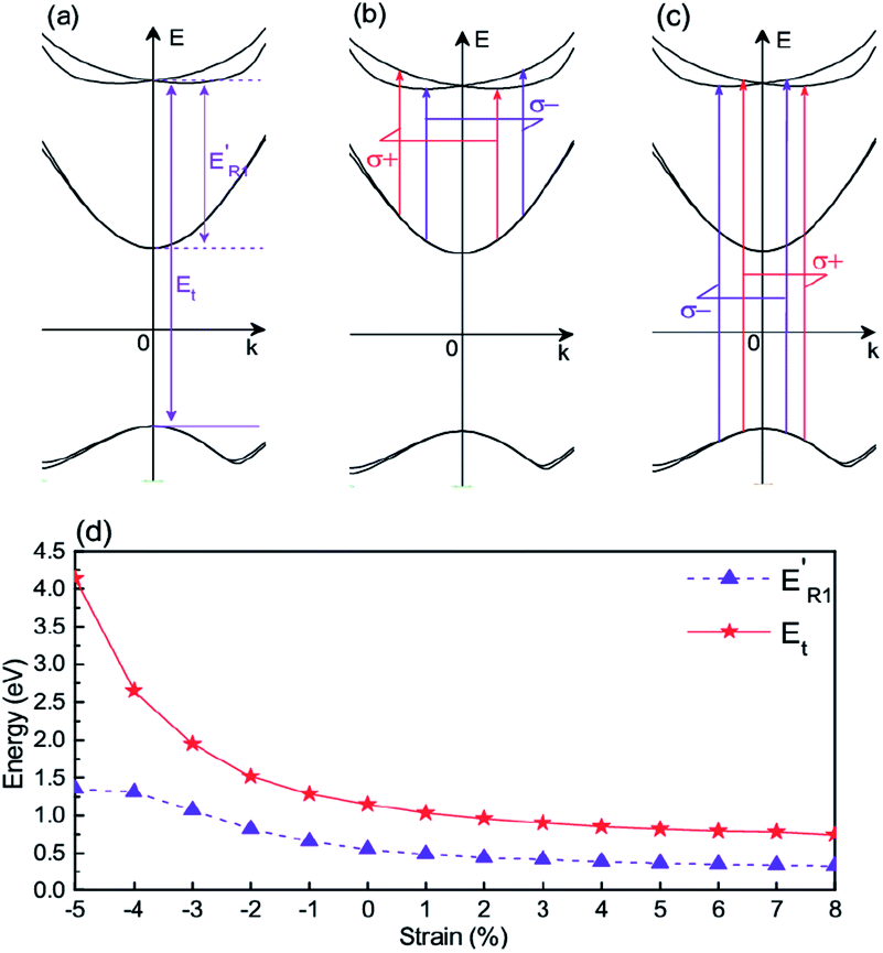 | ||
Fig. 6 Schematic for CPGE: photon energy for transition from the valence band edge (Et) or from the conduction band edge 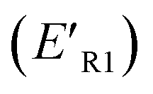 to the Rashba bands (a); the two permitted transitions (only two kx values, kx±, for a given ky) from the conduction band edge through circularly polarized light with σ+ (red) or σ− (purple) (b), and the similar transitions from the valence band edge (c); and the strain dependence of the needed photon energies to the Rashba bands (a); the two permitted transitions (only two kx values, kx±, for a given ky) from the conduction band edge through circularly polarized light with σ+ (red) or σ− (purple) (b), and the similar transitions from the valence band edge (c); and the strain dependence of the needed photon energies  and Et (d). and Et (d). | ||
For generating a net spin-polarized photocurrent, both circularly-polarized light and the Rashba split bands are necessary.18 Upon illumination with a circularly polarized light with photon energy ℏω and given helicity, the energy and angular momentum conservations require that the transition happens only at the two asymmetric k values: kx+ and kx−.18 This makes the average electron velocity in the excited state become nonzero and the contributions of kx± photoelectrons to the current do not cancel each other.18 Changing the photon helicity from +1 to −1 inverts the current because the “center-of-mass” for this transition is shifted in the opposite direction. This results in the generation of the spin polarized CPGE current of the Rashba split dyz/dxz bands, as shown in Fig. 6(b and c). The photon energies needed for the CPGE from the valence band edge (Et) and the conduction band edge  are shown in Fig. 6(d). In principle,18,57,58 it can be described by j = γêE2Pcirc, where γ is the second-rank pseudotensor, E is the amplitude of the electric field of the light, ê is the unit vector pointing in the direction of the light propagation and Pcirc is the helicity of the light beam, and the pseudotensor γ has non-zero element for the C4v point group, which results in a non-zero spin-polarized photoelectron current.19,59,60
IV. Conclusion
In summary, through the first-principles calculations, we have systematically investigated the effect of the biaxial stress on the Rashba spin splitting of the KTO slabs for modelling strained KTO (001) ultrathin films with the most stable surfaces.33,34 The calculated results reveal that tensile in-plane strain changes the Rashba spin splitting little, but the Rashba spin splitting energy ER increases with compressive stress increasing, which is in reasonable agreement with recent experimental result. When the compressive in-plane strain approaches εs = −5%, ER is 140 meV and the k vector offset is kR = 0.21 Å−1, which corresponds to a large Rashba coupling constant 1.3 eV Å. Our analysis indicates that the enhanced giant Rashba spin splitting energy can be attributed to the strong out-of-plane electric field generated by the large compressive biaxial stress. Our further calculations show that the Rashba spin splitting energy can be enhanced to the record 190 meV by adding a STO capping layer. We also show that such giant Rashba effect can be used to generate spin-polarized photocurrents in terms of the circular photogalvanic effect.18–23 Therefore, these giant Rashba phenomena may open a new door to promising spintronic and optoelectronic applications.Conflicts of interest
There are no conflicts to declare.Acknowledgements
This work is supported by Department of Science and Technology of China (Grant No. 2016YFA0300701), Nature Science Foundation of China (Grant No. 11974393 and 11574366), and the Strategic Priority Research Program of the Chinese Academy of Sciences (Grant No. XDB33000000). The calculations were performed in the Milky Way #2 supercomputer system at National Supercomputer Center of Guangzhou, Guangzhou, China.References
- E. I. Rashba, Sov. Phys. Solid State, 1960, 2, 1109 Search PubMed.
- Y. A. Bychkov and E. I. Rashba, J. Phys. C: Solid State Phys., 1984, 17, 6039 Search PubMed.
- Y. A. Bychkov and E. I. Rashba, JETP Lett., 1984, 39, 78 Search PubMed.
- M. O. Nestoklon, E. L. Ivchenko, J.-M. Jancu and P. Voisin, Phys. Rev. B: Condens. Matter Mater. Phys., 2008, 77, 155328 Search PubMed.
- E. Lesne, Y. Fu, S. Oyarzun, J. C. Rojas-Sánchez, D. C. Vaz, H. Naganuma, G. Sicoli, J.-P. Attané, M. Jamet, E. Jacquet, J.-M. George, A. Barthélémy, H. Jaffrès, A. Fert, M. Bibes and L. Vila, Nat. Mater., 2016, 15, 1261 Search PubMed.
- J. Nitta, T. Akazaki, H. Takayanagi and T. Enoki, Phys. Rev. Lett., 1997, 78, 1335 Search PubMed.
- A. D. Caviglia, M. Gabay, S. Gariglio, N. Reyren, C. Cancellieri and J.-M. Triscone, Phys. Rev. Lett., 2010, 104, 126803 Search PubMed.
- K. Premasiri, S. K. Radha, S. Sucharitakul, U. R. Kumar, R. Sankar, F.-C. Chou, Y.-T. Chen and X. P. A. Gao, Nano Lett., 2018, 18, 4403 Search PubMed.
- N. Yu, J. Yuan, K. Li and J. Wang, Appl. Surf. Sci., 2018, 427, 10 Search PubMed.
- M. A. U. Absor, I. Santoso, Harsojo, K. Abraha, H. Kotaka, F. Ishii and M. Saito, Phys. Rev. B, 2018, 97, 205138 Search PubMed.
- Q. Liu, Y. Guo and A. J. Freeman, Nano Lett., 2013, 13, 5264 Search PubMed.
- L. Zhu, T. Zhang, G. Chen and H. Chen, Phys. Chem. Chem. Phys., 2018, 20, 30133 Search PubMed.
- Q. Zhang and U. Schwingenschlögl, Phys. Rev. B, 2018, 97, 155415 Search PubMed.
- S. Singh and A. H. Romero, Phys. Rev. B, 2017, 95, 165444 Search PubMed.
- S.-H. Zhang and B.-G. Liu, Phys. Rev. B, 2019, 100, 165429 Search PubMed.
- Z. Kovacs-Krausz, A. M. Hoque, P. Makk, B. Szentpeteri, M. Kocsis, B. Fulop, M. V. Yakushev, T. V. Kuznetsova, O. E. Tereshchenko, K. A. Kokh, I. E. Lukacs, T. Taniguchi, K. Watanabe, S. P. Dash and S. Csonka, Nano Lett., 2020, 20, 4782 Search PubMed.
- D. Culcer, A. C. Keser, Y. Q. Li and G. Tkachov, 2D Mater., 2020, 7, 022007 Search PubMed.
- S. D. Ganichev, E. L. Ivchenko, S. N. Danilov, J. Eroms, W. Wegscheider, D. Weiss and W. Prettl, Phys. Rev. Lett., 2001, 86, 4358 Search PubMed.
- M. M. R. Moayed, T. Bielewicz, M. S. Zöllner, C. Herrmann and C. Klinke, Nat. Commun., 2017, 8, 15721 Search PubMed.
- Y. Zhang, T. Holder, H. Ishizuka, F. de Juan, N. Nagaosa, C. Felser and B. H. Yan, Nat. Commun., 2019, 21, 3783 Search PubMed.
- H. T. Duc, C. Ngo and T. Meier, Phys. Rev. B, 2019, 100, 045308 Search PubMed.
- M. Chen, K. Lee, J. Li, L. Cheng, Q. Wang, K. Cai, E. E. M. Chia, H. Chang and H. Yang, ACS Nano, 2020, 14, 3539 Search PubMed.
- D. Rees, K. Manna, B. Lu, T. Morimoto, H. Borrmann, C. Felser, J. E. Moore, D. H. Torchinsky and J. Orenstein, Sci. Adv., 2020, 6, eaba0509 Search PubMed.
- P. D. C. King, R. H. He, T. Eknapakul, P. Buaphet, S.-K. Mo, Y. Kaneko, S. Harashima, Y. Hikita, M. S. Bahramy, C. Bell, Z. Hussain, Y. Tokura, Z.-X. Shen, H. Y. Hwang, F. Baumberger and W. Meevasana, Phys. Rev. Lett., 2012, 108, 117602 Search PubMed.
- A. F. Santander-Syro, C. Bareille, F. Fortuna, O. Copie, M. Gabay, F. Bertran, A. Taleb-Ibrahimi, P. Le Fèvre, G. Herranz, N. Reyren, M. Bibes, A. Barthélémy, P. Lecoeur, J. Guevara and M. J. Rozenberg, Phys. Rev. B: Condens. Matter Mater. Phys., 2012, 86, 121107 Search PubMed.
- H. Zhang, X. Yan, X. Zhang, S. Wang, C. Xiong, H. Zhang, S. Qi, J. Zhang, F. Han, N. Wu, B. Liu, Y. Chen, B. Shen and J. Sun, ACS Nano, 2019, 13, 609 Search PubMed.
- H. Zhang, Y. Yun, X. Zhang, H. Zhang, Y. Ma, X. Yan, F. Wang, G. Li, R. Li, T. Khan, Y. Chen, W. Liu, F. Hu, B. Liu, B. Shen, W. Han and J. Sun, Phys. Rev. Lett., 2018, 121, 116803 Search PubMed.
- N. Wadehra, R. Tomar, R. Varma, R. Gopal, Y. Singh, S. Dattagupta and S. Chakraverty, Nat. Commun., 2020, 11, 874 Search PubMed.
- S. Goyal, N. Wadehra and S. Chakraverty, Adv. Mater. Interfaces, 2020, 7, 2000646 Search PubMed.
- K. V. Shanavas and S. Satpathy, Phys. Rev. Lett., 2014, 112, 086802 Search PubMed.
- J. Xi, H. Xu, Y. Zhang and W. J. Weber, Phys. Chem. Chem. Phys., 2017, 19, 6264 Search PubMed.
- X.-J. Zhang and B.-G. Liu, Phys. Chem. Chem. Phys., 2018, 20, 24257 Search PubMed.
- M. Setvin, M. Reticcioli, F. Poelzleitner, J. Hulva, M. Schmid, L. A. Boatner, C. Franchini and U. Diebold, Science, 2018, 359, 572 Search PubMed.
- Y. Wang, J. Cheng, M. Behtash, W. Tang, J. Luo and K. Yang, Phys. Chem. Chem. Phys., 2018, 20, 18515 Search PubMed.
- P. Hohenberg and W. Kohn, Phys. Rev., 1964, 136, B864 Search PubMed.
- W. Kohn and L. J. Sham, Phys. Rev., 1965, 140, A1133 Search PubMed.
- G. Kresse and D. Joubert, Phys. Rev. B: Condens. Matter Mater. Phys., 1999, 59, 1758 Search PubMed.
- P. E. Blöchl, Phys. Rev. B: Condens. Matter Mater. Phys., 1994, 50, 17953 Search PubMed.
- J. P. Perdew, K. Burke and M. Ernzerhof, Phys. Rev. Lett., 1996, 77, 3865 Search PubMed.
- J. P. Perdew, A. Ruzsinszky, G. I. Csonka, O. A. Vydrov, G. E. Scuseria, L. A. Constantin, X. Zhou and K. Burke, Phys. Rev. Lett., 2008, 100, 136406 Search PubMed.
- V. I. Anisimov, F. Aryasetiawan and A. Lichtenstein, J. Phys.: Condens. Matter, 1997, 9, 767 Search PubMed.
- B. Lennart, Phys. Rev. B: Condens. Matter Mater. Phys., 1999, 59, 12301 Search PubMed.
- R. Peng, X. P. Shen, X. Xie, H. C. Xu, S. Y. Tan, M. Xia, T. Zhang, H. Y. Cao, X. G. Gong, J. P. Hu, B. P. Xie and D. L. Feng, Phys. Rev. Lett., 2014, 112, 107001 Search PubMed.
- D.-H. Choe, D. West and S. Zhang, Phys. Rev. Lett., 2018, 121, 196802 Search PubMed.
- C. Cancellieri, D. Fontaine, S. Gariglio, N. Reyren, A. D. Caviglia, A. Fête, S. J. Leake, S. A. Pauli, P. R. Willmott, M. Stengel, P. Ghosez and J.-M. Triscone, Phys. Rev. Lett., 2011, 107, 056102 Search PubMed.
- N. Wadehra, R. Tomar, S. Halder, M. Sharma, I. Singh, N. Jena, B. Prakash, A. De Sarkar, C. Bera, A. Venkatesan and S. Chakraverty, Phys. Rev. B, 2017, 96, 115423 Search PubMed.
- C. Xia, W. Xiong, J. Du, T. Wang, Y. Peng and J. Li, Phys. Rev. B, 2018, 98, 165424 Search PubMed.
- W. Meevasana, P. D. C. King, R. H. He, S.-K. Mo, M. Hashimoto, A. Tamai, P. Songsiriritthigul, F. Baumberger and Z.-X. Shen, Nat. Mater., 2011, 10, 114 Search PubMed.
- Z. Zhong, L. Si, Q. Zhang, W.-G. Yin, S. Yunoki and K. Held, Adv. Mater. Interfaces, 2015, 2, 1400445 Search PubMed.
- K. Ishizaka, M. S. Bahramy, H. Murakawa, M. Sakano, T. Shimojima, T. Sonobe, K. Koizumi, S. Shin, H. Miyahara, A. Kimura, K. Miyamoto, T. Okuda, H. Namatame, M. Taniguchi, R. Arita, N. Nagaosa, K. Kobayashi, Y. Murakami, R. Kumai, Y. Kaneko, Y. Onose and Y. Tokura, Nat. Mater., 2011, 10, 521 Search PubMed.
- J. Krempaský, H. Volfová, S. Muff, N. Pilet, G. Landolt, M. Radović, M. Shi, D. Kriegner, V. Holý, J. Braun, H. Ebert, F. Bisti, V. A. Rogalev, V. N. Strocov, G. Springholz, J. Minár and J. H. Dil, Phys. Rev. B, 2016, 94, 205111 Search PubMed.
- M. Kim, J. Ihm and S. B. Chung, Phys. Rev. B, 2016, 94, 115431 Search PubMed.
- Y. Ma, Y. Dai, W. Wei, X. Li and B. Huang, Phys. Chem. Chem. Phys., 2014, 16, 17603 Search PubMed.
- Y.-H. Meng, W. Bai, H. Gao, S.-J. Gong, J.-Q. Wang, C.-G. Duan and J.-H. Chu, Nanoscale, 2017, 9, 17957 Search PubMed.
- L. G. D. da Silveira, P. Barone and S. Picozzi, Phys. Rev. B, 2016, 93, 245159 Search PubMed.
- S. Thiel, G. Hammerl, A. Schmehl, C. W. Schneider and J. Mannhart, Science, 2006, 313, 1942 Search PubMed.
- S. Zhang, N. Tang, W. Jin, J. Duan, X. He, X. Rong, C. He, L. Zhang, X. Qin, L. Dai, Y. Chen, W. Ge and B. Shen, Nano Lett., 2015, 15, 1152 Search PubMed.
- H. Yuan, X. Wang, B. Lian, H. Zhang, X. Fang, B. Shen, G. Xu, Y. Xu, S.-C. Zhang, H. Y. Hwang and Y. Cui, Nat. Nanotechnol., 2014, 9, 851 Search PubMed.
- S. Vajna, E. Simon, A. Szilva, K. Palotas, B. Ujfalussy and L. Szunyogh, Phys. Rev. B: Condens. Matter Mater. Phys., 2012, 85, 075404 Search PubMed.
- L. E. Golub, E. L. Ivchenko and B. Z. Spivak, JETP Lett., 2017, 105, 782 Search PubMed.
Footnote |
| † Present affiliation: Institute for Advanced Simulation, Forschungszentrum Jülich, D-52425 Jülich, Germany. |
| This journal is © The Royal Society of Chemistry 2020 |