
 Open Access Article
 This Open Access Article is licensed under a Creative Commons Attribution-Non Commercial 3.0 Unported Licence
Active site-dominated electromagnetic enhancement of surface-enhanced Raman spectroscopy (SERS) on a Cu triangle plate†
Chang Li *abc and
Mingqiang Chenabc
*abc and
Mingqiang Chenabc
aAnalytical and Testing Center, Anhui University of Science and Technology, 232001, Huainan, China. E-mail: cli@aust.edu.cn; Tel: +86 13564095689
bSchool of Chemical Engineering, Anhui University of Science and Technology, 232001, Huainan, PR China
cSchool of Earth Science and Environmental Engineering, Anhui University of Science and Technology, 232001, Huainan, PR China
First published on 18th November 2020
Abstract
Revealing the sensitivity and selectivity of the Raman enhancement mechanism is extremely significant for disease diagnosis, environmental surveillance, and food safety supervision. In this study, chemical erosion copper triangle plates (CTPs) were employed as SERS substrate to detect the rhodamine B (Rh B) probe molecule at different etching times. A simple and cost-effective method affords unique insights into the surface enrichment of analytes, which could facilitate the high-performance SERS analysis of numerous analytes. The relationship between the Raman intensity and the concentration of Rh B follows the Freundlich model, which means that the wet-etching surface can create SERS-active site attachment Rh B molecules on the CTPs. The morphology of CTPs was modified by H2O2/HCl etchants; however, the composition of CTPs remained stable without oxidation. This proposes that the largest contribution to the enhancement was the hot-spots that can produce surface plasma resonance on the CTPs. The number of hot-spots can be intelligently adjusted by the artificial control of the surface morphology of metal materials, providing an unambiguous improvement in the SERS sensitivity and capability.
Introduction
The Raman scattering signals carrying the fingerprint information of molecules with high spectral resolution and sensitivity can be applied in the fields of catalysis,1 sensing,2–6 chemical analysis,7–9 environment monitoring.10 However, the weak Raman scattering intensity of pure substances limits its scope of comprehensive application. Surface-enhanced Raman spectroscopy (SERS) is a powerful and effective non-destructive strategy to further strengthen Raman scattering.11–13 A copper substrate is an ideal SERS candidate owing its low cost, improved physical stability, and high electromagnetic enhancement performance14,15 compared with the silver system that is considered to have a higher enhancement factor (EF). In particular, the bactericidal properties of silver will cause undesired biological destruction;16 thus, also in that sense, copper is advantageous over silver. Moreover, the fabrication of hot spots on gold surface controllably by anisotropic etching requires harsh implementation conditions for the stability of elemental gold.17 Therefore, the low-priced copper SERS substrate is more suitable for etching under mild etching reaction environment.18As the large smooth surface is not conducive to the enhancement of Raman scattering, chemical bottom-up colloid systems are investigated to improve the SERS application.19 The morphology, roughness, and cluster aggregation of different copper materials may lead to distinguishing from enhancement factors (EFs).20,21 Spherical- and rod-copper nanoparticles surface modified by poly(allylamine) were used as SERS-active substrates with EFs in the order of 104.22 Laser ablation core–shell copper can obtain SERS-active colloidal suspension without reducing agents.23 Porous copper membranes formed by the sacrificial template method can lower the costs of SERS substances with mass production.24 Five-fold copper nanowires prepared by the solvothermal method obtained an EF value of 1.1 × 10⁴ for 4-mercaptobenzoic acid.25 The thermal annealing copper array showed high SERS activity with EFs in the order of 107.26 Copper nanowire-coated carbon fibers using electrochemical deposition obtained SERS EF of the order 106 to 107.27 Dual-functional porous copper films modulated via a dynamic hydrogen bubble template show high sensitivity, excellent activity, and good reproducibility for SERS detection.1 Fabricated superhydrophobic nanostructured copper shows a low detection limit of 10−13 M with an EF of ∼1.2 × 105.28 The methods all above intend to increase the number of hot spots for the formation of the plasmon gaps between or inside the boundaries of the metal surface induced by the electromagnetic surface plasmon resonance, which can influence the SERS-physical enhancement. However, it is still not fully understood how nanogaps of the rough copper nanomaterials to enhance the molecular Raman scattering quantitatively.
The long-range electromagnetic enhancement (EM) makes a major contribution to the noble metal SERS phenomenon. When incident light illuminates the rough surface, it causes collective oscillations of the metal surface electrons, which is termed as surface plasmon resonance (SPR). The redistribution of the local field and a great enhancement of the EM field at a specific position (called a “hot spots”) were formed during the exciting electric field process. To understand the relationship between the number of hot spots and the Raman scattering intensity is of great significance to improve the SERS properties of metal materials.
Herein, we developed a copper triangle plate (CTP) utilizing a facile chemical reduction in solutions.29 Then, the roughness surface of CTP was formed by chemical etching with the HCl/H2O2 system to create more hot-spots. Rhodamine B (Rh B)30,31 loaded on the CTP surface roughness varied with different etching times was selected as a probe molecule to measure the SERS activity. During the etching process, the surface roughness of those CTPs was altered; the optical property of those CTPs was widely tuned and the enhancement of SERS capabilities was largely associated with the reaction time of etchants.
Methods
Copper triangle plate preparation
Cu(II) nitrate trihydrates (Cu(NO3)2·3H2O, ≥99%), L-ascorbic acid (≥99%), cetyltrimethylammonium bromide (CTAB, ≥99%), and hexamethylenetetramine (HMTA, ≥99%) were purchased from Sinopharm Chemical Reagent Co., Ltd. All chemicals were used as received without further purification. In a typical synthesis experiment,27 Cu(NO3)2·3H2O (50 mg) and L-ascorbic acid (100 mg) were dissolved with 15 mL of deionized water in a glass vial (20 mL). After forming a homogeneous solution, CTAB (100 mg) and HMTA (100 mg) were added. After 30 min of stirring, the vial of the solution was capped and heated from room temperature to 80 °C and kept at 80 °C for 6 h in a water bath. The products were collected by centrifugation at 10![[thin space (1/6-em)]](https://www.rsc.org/images/entities/char_2009.gif) 000 rpm and washed three times ethanol.
000 rpm and washed three times ethanol.
Wet-etching copper triangle plate
Hydrochloric acid (HCl, 36%) and perhydrol (H2O2, 30%) were purchased from Sinopharm Chemical Reagent Co., Ltd. All chemicals were used as received without further purification. The final concentrations of HCl and H2O2 diluted by deionized water are both 1 g L−1 in the etching solution. To prepare the etching samples, 1 mg of as-synthesized CTP and 2 mL of deionized water was first mixed and sonicated. ∼10 μL of CTP solution was then loaded onto a single side polishing silicon wafer (5 cm × 5 cm) surface. After evaporating the water at 60 °C in an oven for 2 h, the CTP layer formed on the silicon wafer. The etching solution (∼5 μL) was dropcasted onto the silicon wafer-supported CTP film for etching 4 min (CTP-4), 10 min (CTP-10) and 15 min (CTP-15). The etching solution was then sucked away using a filter paper and the etching samples were washed by deionized water eventually. The non-etched CTP was named as CTP-0.Material characterization
TEM images were taken with an FEI TF20 at an acceleration voltage of 200 kV. SEM images were recorded on a Hitachi FlexSEM 1000. EDX was performed on an IXRF Model 550i. AFM measurements were performed on a Dimension Icon (Bruker) to obtain 3D profiles of the patterns. X-ray photoelectron spectrometry (XPS) surveys were gathered on a Thermo Fisher ESCALAB 250Xi+. The adventitious carbon peak was calibrated to 284.8 eV. A Rigaku Smartlab SE system was used to obtain the XRD patterns. Fourier transform infrared spectroscopy (FT-IR) was performed using Thermo Fisher Nicolet iS50.Raman measurement
To study the Raman enhancement effected by the chemical etching CTP, rhodamine B (Rh B, ≥99%, Sinopharm Chemical Reagent Co., Ltd.), rhodamine 6G (Rh 6G, ≥99%, Sino Pharm Chemical Reagent Co., Ltd.), crystal violet (CV, ≥99%, Sinopharm Chemical Reagent Co., Ltd.) and methylene blue (MB, ≥99%, Sinopharm Chemical Reagent Co., Ltd.) were dissolved with deionized water to obtain the final concentration of 10−3 M solution. The four kinds of probe molecules were used as SERS-probes in the preliminary screening experiment. Then, the Rh B solution was diluted to 10−4 M, 10−5 M, 10−6 M and 10−7 M, respectively. The silicon wafers loaded with CTP-0, CTP-4, CTP-10 and CTP-15 were immersed in a certain concentration of the probe molecular solution to absorb the molecule for 5 h in a glass vial. To get rid of excess moisture, the samples were dried in an oven for 2 h finally. The Raman spectra were subsequently collected using a high-resolution confocal Raman spectrometer (Renishaw inVia Raman microscope). The excitation wavelength was 785 nm.32 Moreover, a ×50 L objective was used to focus the laser beam. The spectra were acquired for 10 s without accumulations and the laser power was maintained at 0.3 mW with an average spot size of 1 μm in diameter in all acquisitions. For each sample, Raman spectra from ten different areas were collected, and the signal intensity was averaged for final analysis.Results and discussion
The freshly prepared copper triangle plate (CTP) was synthesized by chemically reducing Cu(II) nitrate trihydrate using L-ascorbic acid with the surfactant present of CTAB and HMTA following the literature.29 To improve the size and the thickness of CTP for making chemical erosion easier and obvious, the time of the water bath kept to 6 h during the triangle plate growth process. The CTPs have equilateral triangle morphologies with edge lengths ranging from 4 μm to 10 μm, as shown in Fig. 1A and B. From the further analysis with the X-ray diffraction (XRD) pattern in Fig. 1C, the structure of the CTP is face-centered cubic single crystallinity with sharp X-ray diffraction peaks. Compared to the other two peaks, (200) and (220), the (111) peak intensity enhancement indicated that the orient {111} planes were parallel to the silicon wafer when a large number of CTPs stacked face to face on the silicon substrate.29 The two sharp characteristic peaks appearing at 932.6 eV and 952.5 eV without other oxidation peaks indicated that Cu(II) nitrate trihydrate has been completely reduced to Cu(0), as shown in the narrow XPS spectra of CTP in Fig. 1D. CTP with a simple and definite composition is more beneficial to the study of Raman enhancement through morphology modified by etching.33 | ||
| Fig. 1 Characterization and SERS selectivity of the copper triangle plate (CTP). (A) SEM and (B) TEM images showing the size and morphology of CTP. (C) XRD pattern of CTP with peaks (111), (200) and (220). (D) The narrow XPS survey of CTP. (E) The Raman spectrum and their structure formula of Rh B, Rh 6G, CV and MB. | ||
The same concentration (10−3 M) of Rh B, Rh 6G, CV and MB was dispersed on the CTP substrate as the Raman probe molecule to identify the Raman scattering selectivity of CTP (Fig. 1E). The characteristic Raman shifts peaks and their assignments of the four types of probe molecules are shown in Tables S1 and S2, ESI.† The Rh B molecule has the strongest Raman scattering intensity and excellent Raman shift resolution (red, Fig. 1E). The Raman intensity and shift of Rh 6G with a similar structure were still with clear and easily recognizable curve outline (blue, Fig. 1E); however, the Raman resolution and intensity of the CV (violet, Fig. 1E) and MB (black, Fig. 1E) curves are too poor, making it difficult to separate and recognize the peaks. The asymmetric multi-ring structure makes the Raman enhancement of Rh B and Rh 6G more sensitive than the symmetric structure of CV and MB (structural formulas of the four dye molecules are shown on the right of the Fig. 1E).
Compared with the large-scale copper plate (ESI Fig. 1†), the CTP substrate has excellent Raman enhancement performance for Rh B. The as-synthesized CTP was etched using the HCl/H2O2 system without creating any new species because the oxidized copper can be totally dissolved in the HCl solution. The dye molecule Rh B with remarkable Raman scattering absorption peaks was dispersed on an etched CTP surface for detecting the quantitative variation of SERS-active sites during the etching process. The structural evolution of CTP was investigated using SEM, as shown in Fig. 2A. CTP without etching has a smooth surface (0 min, Fig. 2A). After etching for 4 min, a lot of pits and gaps formed on the surface of CTP, which indicated that parts of copper were removed by etchants (4 min, Fig. 2A). With more copper being ionized, the surface became rough while still retaining triangle shapes (10 min, Fig. 2A). However, the edge and corner of CTP were defected with further corroding and even some small particles, which may be the undissolved copper fragments appeared on the CTP surface (15 min, Fig. 2A). CTP samples etched at different times named CTP-0, CTP-4, CTP-10 and CTP-15 were selected as the Raman substrate for Raman measurement, respectively. The Raman spectra of Rh B on CTP at the concentration of 10−4 M, 10−5 M, 10−6 M and 10−7 M are exhibited in Fig. 2B. The Raman shifts of the C–C stretching vibration mode, C–H stretching, aromatic C–C bending and C–H bending are at 1649 cm−1, 1527 cm−1, 1360 cm−1 and 1281 cm−1, respectively. Compared with pure Rh B (blank) without the CTP substrate, the Raman scattering signal is all enhanced after using CTP as the SERS substance for the four different concentrations, which indicated that CTP can improve the Raman signal intensity. Notice that the Raman intensity increased first with the etching time (CTP-4 and CTP-10) and decreased later by longer etching time (CTP-15), which means the etching time can influence the enhancement degree. Moreover, if we reduced the concentration of Rh B, the correspondent intensity of the Raman signal would decrease again. Note that if the concentration drops too low, the resolution of the peaks will become poor.
 | ||
| Fig. 2 Etching process and Raman measurement of CTPs. (A) SEM images of CTP at different etching times. (B) The Raman spectrum of Rh B on the CTP substance at different concentrations of Rh B: (a) 10−4 M, (b) 10−5 M, (c) 10−6 M and (d) 10−7 M. | ||
We attempt to follow the electromagnetic mechanism34 to explain the SERS activity of etching CTP. We proposed that only the probe molecular attachment to the hot spots will create surface plasmon resonance induced by laser, which can improve the Raman scattering signal. More hot spots were produced with the initial etching (CTP-4 and CTP-10); however, hot spots decreased with excessive etching (CTP-15). The 3D AFM profile shows the ravinement-like surface of CTP formation after 10 min etching, compared with CTP-0 shown in Fig. 3A. The gaps among the raised parts on the surface were the main points for hot spots. Compared with non-etched CTP, the etched CTP still has a simple component without the copper oxide species, as the XPS shown (Fig. 3B). The XPS narrow spectrum of CTP-10 also showed two sharp peaks, which indicated the CTP was still zero valent copper after etching.
 | ||
| Fig. 3 Formation of hot spots and its influence for Raman enhancement (A) AFM 3D pattern of CTP-0 and CTP-10 (B). UPS spectrum of CTP-10. (C) The relationship between the Raman signal and the Rh B concentration at 1649 cm−1. The data can be fitted by the Freundlich model. (D) The EF value of CTP as a function vs. time at different Rh B concentrations. (a) The EF collection at P1 (1649 cm−1). (b) The EF collection at P2 (1527 cm−1). | ||
The Freundlich model could describe the relationship between the intensity of the Raman signal and the Rh B concentration as the following:35
|
logISERS = h + klogCRh B
| (1) |
To further study the Raman enhancement capability, the enhancement factors (EFs) of CTP-0 to 15 (details can be seen in S1 ESI†) were calculated at 1649 cm−1 (P1) and 1527 cm−1 (P2) shown in Fig. 3D. The EFs of CTP-10 at each concentration were the largest values of all, which means that the 10 min etching on CTP can create the most of hot spots with CTP still maintaining a triangle shape. The EFs of Rh B at 10−6 M were the largest and the EFs would become weak if the Rh B concentration continued decreasing. Compared with P1, the EF of P2 has a similar tendency just with weaker enhancement strength decided by the Rh B inner molecular structure. The optimum chemical etched CTP can obtain the EF value of five times than the non-etched CTP.
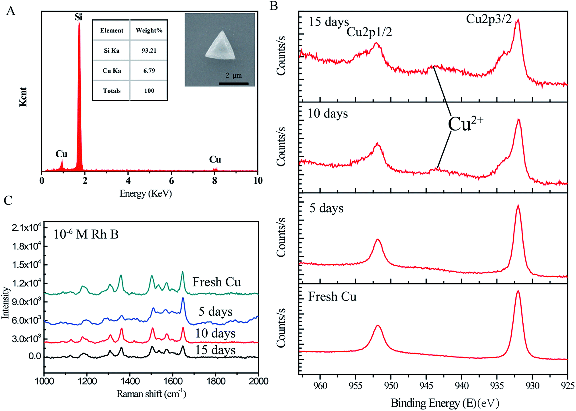
The EDX of a single CTP-10 dispersed on the silicon wafer shows copper is still the only component after etching in Fig. 4A. To estimate the reproducibility and stability of CTP, CTP-10 was stored in air at the room temperature for 5 days, 10 days and 15 days, respectively. Then, they were sent to measure the XPS and SERS tests shown in Fig. 4B and C. After standing for 10 days and 15 days, the characteristic peak of divalent copper ions appeared at 943 eV, which cannot be found from the fresh CTP-10 and the CTP-10 standing for 5 days. The copper was partially oxidized when the CTP was exposed to the air for a long time. Simultaneously, the Raman intensity of the samples containing Cu2+ decreased slightly shown in Fig. 4C. It is concluded that under our experimental conditions, the strengthening effect of pure copper is better for SERS substrates.
 | ||
| Fig. 4 The purity and stability of CTP for SERS. (A) EDX of fresh CTP-10 (etching for 10 min). (B) The XPS survey of CTP-10 standing in air for 0 days, 5 days, 10 days and 15 days. (C) The Raman spectrum of Rh B on the CTP-10 substances standing in air for different days at 10−6 M. | ||
Although surface plasmon resonance on the copper surface played a major role to improve the CTP SERS activity with the analysis above, the chemical enhancement of CTP was still discussed in Fig. 5. The ultraviolet photoelectron spectroscopy (UPS) of optimum CTP-10 was scanned to obtain the valence band spectrum with the valence bandwidth 16.86 eV. The work function (vs. vacuum) of CTP-10 was 4.36 eV calculated from the total energy of ultraviolet light being 21.22 eV. The match ability of the band structure of CTP, and the lowest unoccupied molecular orbit (LUMO) and highest occupied molecular orbit (HOMO) levels of Rh B molecules were demonstrated in Fig. 4B. The work function of CTP-10 (EF = −4.36 eV vs. vacuum) was located between LUMO orbit (ELUMO = −2.73 eV vs. vacuum) and HUMO orbit (ELUMO = −4.97 eV vs. vacuum).23 Among the SERS chemical enhancement including resonance Raman enhancement (μRRE) of Rh B, ground state chemical enhancement (μGSCE) and charge-transfer resonance enhancement (μCTRE), the charge transfer resonance (μCTRE) is considered as the major contributor.36
 | ||
| Fig. 5 The band structure of CTP for chemical enhancement. (A) UPS and XPS spectra of CTP-10. (B) The scheme showing the proposed mechanism for the chemical enhanced CTP. | ||
The charge transfer resonance may take place at each etched CTP, which indicates that it has the same contribution for the EF enhancement under our experimental conditions. It is further proved that the hot spots increasing on the CTP surface after etching were the key factors to improve the SERS capabilities of copper.
Conclusion
In summary, the as-prepared CTP etched by the H2O2/HCl etchants shows excellent SERS activity for Rh B with the EF at the value of 4.5 × 10⁶. To extend the etching time, the hot spots (SERS-active sites) increasing initially and then decreasing will lead to the results of Raman enhancement, which has a corresponding trend of the curve. Our experimental data matched the Freundlich model perfectly, which indicates that the hot spot dominated electromagnetic enhancement was the main Raman enhancement mechanism of rough copper. Etched CTPs were highly sensitive SERS platforms with good stability and reproducibility.Conflicts of interest
The authors declare no competing financial interest.Acknowledgements
This work thanks for the supports of the school level project of Anhui University of Science and Technology (QN2019106).References
- H. Yang, X. Hao, J. Tang, W. Jin, C. Liu, H. Hou, X. Ji and J. Hu, Appl. Surf. Sci., 2019, 494, 731–739 CrossRef CAS.
- S. Cong, Y. Yuan, Z. Chen, J. Hou, M. Yang, Y. Su, Y. Zhang, L. Li, Q. Li and F. Geng, Nat. Commun., 2015, 6, 1–7 Search PubMed.
- P. Karthick Kannan, P. Shankar, C. Blackman and C. H. Chung, Adv. Mater., 2019, 31, e1803432 CrossRef.
- A. A. Kowalska, A. Kaminska, W. Adamkiewicz, E. Witkowska and M. Tkacz, J. Raman Spectrosc., 2015, 46, 428–433 CrossRef CAS.
- J. Wu, H.-Y. Chen, N. Yang, J. Cao, X. Yan, F. Liu, Q. Sun, X. Ling, J. Guo and H. Wang, Nat. Electron., 2020, 3, 466–472 CrossRef CAS.
- Q. Yu, Y. Wang, R. Mei, Y. Yin, J. You and L. Chen, Anal. Chem., 2019, 91, 5270–5277 CrossRef CAS.
- J. Du, Y. Ying, X.-y. Guo, C.-c. Li, Y. Wu, Y. Wen and H.-F. Yang, Int. J. Ind. Chem., 2017, 8, 285–296 CrossRef.
- G. Yuan, D. Lin, Y. Wang, X. Huang, W. Chen, X. Xie, J. Zong, Q.-Q. Yuan, H. Zheng, D. Wang, J. Xu, S.-C. Li, Y. Zhang, J. Sun, X. Xi and L. Gao, Nature, 2020, 577, 204–208 CrossRef CAS.
- Y. Wang, B. Yan and L. Chen, Chem. Rev., 2013, 113, 1391–1428 CrossRef CAS.
- M.-K. Oh, R. De and S.-Y. Yim, J. Raman Spectrosc., 2018, 49, 800–809 CrossRef CAS.
- G. Demirel, H. Usta, M. Yilmaz, M. Celik, H. A. Alidagi and F. Buyukserin, J. Mater. Chem. C, 2018, 6, 5314–5335 RSC.
- R. Hatzenpichler, V. Krukenberg, R. L. Spietz and Z. J. Jay, Nat. Rev. Microbiol., 2020, 18, 241–256 CrossRef CAS.
- S. Bai, D. Serien, A. Hu and K. Sugioka, Adv. Funct. Mater., 2018, 28, 1706262 CrossRef.
- M. Dendisová-Vyškovská, V. Prokopec, M. Člupek and P. Matějka, J. Raman Spectrosc., 2012, 43, 181–186 CrossRef.
- W. Zhang, B. Li, L. Chen, Y. Wang, D. Gao, X. Ma and A. Wu, Anal. Methods, 2014, 6, 2066–2071 RSC.
- C. Douketis, T. L. Haslett, Z. Wang, M. Moskovits and S. Iannotta, J. Chem. Phys., 2000, 113, 11315–11323 CrossRef CAS.
- R. Mei, Y. Wang, Q. Yu, Y. Yin, R. Zhao and L. Chen, ACS Appl. Mater. Interfaces, 2020, 12, 2059–2066 CrossRef CAS.
- D. Xu, J. Dong, S. Zhang and J. Chen, Sens. Actuators, A, 2018, 271, 18–23 CrossRef CAS.
- E. Bozo, A. Dombovari, M. Mohl, V. K. Virtanen, S. Saarakkala, R. Vajtai and K. Kordas, IEEE Sens. J., 2020, 20, 143–148 CAS.
- M. Jahn, S. Patze, I. J. Hidi, R. Knipper, A. I. Radu, A. Mühlig, S. Yüksel, V. Peksa, K. Weber and T. Mayerhöfer, Analyst, 2016, 141, 756–793 RSC.
- K. N. Kanipe, P. P. Chidester, G. D. Stucky, C. D. Meinhart and M. Moskovits, J. Phys. Chem. C, 2017, 121, 14269–14273 CrossRef CAS.
- Y. Wang and T. Asefa, Langmuir, 2010, 26, 7469–7474 CrossRef CAS.
- M. Muniz-Miranda, C. Gellini and E. Giorgetti, J. Phys. Chem. C, 2011, 115, 5021–5027 CrossRef CAS.
- B. Hanna, S. Redko, A. Smirnov, A. Panarin, S. Terekhov, P. Nenzi, M. Balucani and V. Bondarenko, Nanoscale Res. Lett., 2012, 7, 477 CrossRef.
- H.-J. Yang, S.-Y. He and H.-Y. Tuan, Langmuir, 2014, 30, 602–610 CrossRef CAS.
- A. J. Pereira, J. P. Gomes, G. F. Lenz, R. Schneider, J. A. Chaker, P. E. N. de Souza and J. F. Felix, J. Phys. Chem. C, 2016, 120, 12265–12272 CrossRef CAS.
- V. Halouzka, B. Halouzkova, D. Jirovsky, D. Hemzal, P. Ondra, E. Siranidi, A. G. Kontos, P. Falaras and J. Hrbac, Talanta, 2017, 165, 384–390 CrossRef CAS.
- P. Fu, X. Shi, F. Jiang and X. Xu, Appl. Surf. Sci., 2020, 501, 144269 CrossRef CAS.
- W. Luc, X. Fu, J. Shi, J.-J. Lv, M. Jouny, B. H. Ko, Y. Xu, Q. Tu, X. Hu and J. Wu, Nat. Catal., 2019, 2, 423–430 CrossRef CAS.
- H. Zhao, Y. Zhang, G. Li, F. Tian, H. Tang and R. Chen, RSC Adv., 2016, 6, 7772–7779 RSC.
- A. Farag and I. Yahia, Opt. Commun., 2010, 283, 4310–4317 CrossRef CAS.
- A. V. Markin, N. E. Markina, J. Popp and D. Cialla-May, TrAC, Trends Anal. Chem., 2018, 108, 247–259 CrossRef CAS.
- C. Qiu, Y. Bao, N. L. Netzer and C. Jiang, J. Mater. Chem. A, 2013, 1, 8790–8797 RSC.
- S. Y. Ding, E. M. You, Z. Q. Tian and M. Moskovits, Chem. Soc. Rev., 2017, 46, 4042–4076 RSC.
- Y. Lai, C. Wang and H. Shao, ACS Appl. Nano Mater., 2020, 3, 1800–1807 CrossRef CAS.
- X. X. Han, W. Ji, B. Zhao and Y. Ozaki, Nanoscale, 2017, 9, 4847–4861 RSC.
Footnote |
| † Electronic supplementary information (ESI) available: Additional discussions and figures. See DOI: 10.1039/d0ra08477h |
| This journal is © The Royal Society of Chemistry 2020 |