
 Open Access Article
 This Open Access Article is licensed under a
 Creative Commons Attribution 3.0 Unported Licence
Electronic structure and thermoelectric properties of Mo-based dichalcogenide monolayers locally and randomly modified by substitutional atoms†
M. Vallinayagam ab,
M. Posselt*a and
S. Chandra*c
ab,
M. Posselt*a and
S. Chandra*c
aHelmholtz-Zentrum Dresden-Rossendorf, Institute of Ion Beam Physics and Materials Research, Bautzner Landstraße 400, 01328 Dresden, Germany. E-mail: m.posselt@hzdr.de
bTechnische Universität Dresden, 01062 Dresden, Germany
cMaterials Science Group, Indira Gandhi Centre for Atomic Research, HBNI, Kalpakkam 603102, Tamil Nadu, India. E-mail: sharat.c@gmail.com
First published on 26th November 2020
Abstract
Density functional theory and Boltzmann transport equations are used to investigate electronic band structure and thermoelectric (TE) properties of different two-dimensional (2D) materials containing Mo, S, Nb, Se, and Te. In MoS2-based monolayers (MLs) the substitution of S atoms by Te atoms up to the concentration of 12.5 at% leads to a more significant change of the band structure than in the corresponding case with Se atoms. In particular, the bandgap is reduced. At a high concentration of Se or Te the electronic structure becomes more similar to that of the SeMoS or TeMoS Janus layers, and the MoSe2 or MoTe2 MLs. It is found that local and random introduction of substitutional Se or Te atoms yields not very different results. The substitution of Mo by Nb, at the concentration of 2.1 at% leads to hole levels. The thermoelectric properties of the considered 2D materials are quantified by the Seebeck coefficient and thermoelectric figure of merit. The two characteristics are determined for different levels of p- or n-doping of the MLs and for different temperatures. Compared to the pristine MoS2 ML, Te substitutional atoms cause more changes of the thermoelectric properties than Se atoms. However, MLs with Se substitutional atoms show a high thermoelectric figure of merit in a broader range of possible p- or n-doping levels. In most cases, the maximum thermoelectric figure of merit is about one, both in p- and n-type materials, and for temperatures between 300 and 1200 K. This is not only found for MoS2-based MLs with substitutional atoms but also for the Janus layers and for MoSe2 or MoTe2 MLs. Interestingly, for MLs with one Nb as well as two or four Te substitutional atoms the highest values of the TE figure of merit of 1.2 and 1.40, respectively, are obtained at a temperature of 1200 K.
I. Introduction
The direct conversion of heat into electricity is feasible using thermoelectric (TE) materials and creates huge interest in clean energy production. The efficiency of these materials depends mainly on Seebeck coefficient, electrical conductivity, and thermal conductivity.1,2 The TE efficiency can be improved in many aspects such as replacing bulk solids with materials with reduced dimension.1–13 In particular Transition Metal Dichalcogenides (TMD) attract much interest due to the control over the electronic properties via various mechanisms such as compositional modifications,14–19 layer stacking,20,21 applying external fields,22,23 layer interfacing,24 and inducing strain on layers.23,25,26 Depending on the composition TMD show various characteristics such as metallic, semiconducting and superconducting properties.27–32 Therefore, TMD may be interesting for many applications.32–34 TMD are layered bulk material and each layer consist of three atomic planes. Two-dimensional TMD consisting of a monolayers are synthesized from bulk TMD using exfoliation process or chemical treatment on suitable substrate.Dimensionality reduction, from three to two dimension, influences bandgap and may cause indirect to direct bandgap transition.2,6,13,20,35,36 Tuning the electronic properties, which influence carrier concentration and mobility as well as Seebeck coefficient and thermal conductivity, is vital for the TE applications of TMD. Recent theoretical16 and experimental18,37,38 investigations on monolayer (ML) MoS2 with substitutional Se and Te atoms show that the electronic band gap changes due to S–Se and S–Te interactions. The band gap values are in the range of 1.0–1.8 eV.39 On the other hand, Janus MLs have been formed where one of the atomic plane consisting of S is replaced by a plane with other chalcogenides, e.g. Se or Te. Experimental40 and theoretical studies41 were performed to investigate the TE properties of Janus layers XMoX′ (X′ and X may be S, Se, or Te, with X′ ≠ X). Calculations show that Janus MLs XMoX′ but also SePtS have a higher TE performance under applied strain.42,43
Many studies investigated properties of TMD MLs by the introduction of substitutional atoms at different concentrations.16,18,37,39,44 For example, Komsa et al.16 theoretically studied MoS2 MLs with different concentrations of random substitution of S by Se or Te. They showed that MoS2(1−x)Se2x and MoS2(1−x)Te2x MLs are thermodynamically stable and the bandgap changes when Se/Te concentration is varied.16 On the other hand, Feng et al.15,37 succeeded in synthesizing MoS2(1−x)Se2x MLs. They measured the bandgap using photoluminescence spectroscopy.15,37 Using High-Resolution Transmission Electron Microscopy (HRTEM) and Atomic Resolution High-Angle Annular Dark-Field Scanning Transmission Electron Microscopy (HAADF-STEM) they found clusters with different MoS2(1−x)Se2x compositions embedded in the MoS2 ML.15,37
In the present work band structure and TE properties of the pristine MoS2 ML are compared with those of MoS2-based MLs modified by random or local substitution of S by Se or Te. Local substitution means that some or all S atoms which are nearest neighbors of a certain Mo atom are replaced. Obviously, in a real sample, both the random and cluster arrangement of substitutional atoms may exist, and until now it is not clear how the different positions of Se or Te influence band structure and TE properties. Additionally, the substitution of Mo by Nb is considered. Moreover, electronic structure and TE characteristics of SeMoS and TeMoS Janus layers as well as MoSe2 and MoTe2 MLs, with or without Nb substitutional atom are determined. In this manner, the properties of Mo-based dichalcogenide MLs are determined for low to maximum concentration of S substitution by Se or Te, for cases without or with Nb substitution of Mo. To the best of our knowledge, such a comprehensive study has not been performed yet. The results obtained for the different MLs are compared in order to find optimum TE features.
II. Structural models and computational details
The models of pure and compositionally modified MLs are derived from the bulk 2H-MoS2 polymorph which shows P63/mmc symmetry.32 The bulk unit cell has two Mo and four S atoms, which are arranged alternately in 3 planes (2 S planes and one Mo plane in between). Each Mo atom has six nearest S and each S has three nearest Mo atoms, all together forming trigonal prismatic coordination.32 In this work, a supercell based on the pristine MoS2 ML is considered (Fig. 1a). In this supercell, the basic MoS2 ML consists of 4 × 4 MoS2 unit cells, i.e. of 16 Mo and 32 S sites. Three-dimensional periodic boundary conditions are applied. Along the c axis, the distance between the periodic replicas of the MLs is 15 Å so that interlayer interactions are avoided. The following locally modified MoS2-based MLs are investigated: (i) in the pure MoS2 ML one Mo atom is replaced by one Nb atom. This is denoted by MoS2(1-Nb) (Fig. 1b). One Nb atom in the given supercell corresponds to an atomic concentration of about 2.1 at%, due to cell size and periodic boundary conditions. Nb is energetically stable when it occupies Mo sites as demonstrated experimentally by Wu et al.45 (ii) The six S atoms surrounding the substitutional Nb atom are replaced one by one by Se atoms. Here the denotations MoS2(1-Nb,1-Se), …, MoS2(1-Nb,6-Se), or shortly MoS2(1-Nb,1–6-Se), are used. This corresponds to Se concentrations between 2.1 and 12.5 at%. An example is shown in Fig. 1c. (iii) Similarly to Se incorporation, Te atoms are substituted on S sites, which is denoted by MoS2(1-Nb,1–6-Te). Also cases without the Nb substitutional atom, i.e. (iv) MoS2(1–6Se) and (v) MoS2(1–6Te), are studied to determine the effect of Nb. In order to investigate the difference between local and random modification of MoS2 MLs we consider random substitution of 6 S atoms by 6 Se or 6 Te atoms with the denotations MoS2(6-Se,r), MoS2(6-Te,r), MoS2(1-Nb,6-Se,r) and MoS2(1-Nb,6-Te,r), see Fig. 1d. Furthermore, the following Janus MLs are investigated: (i) the S atoms in one atomic plane of the pristine MoS2 ML are replaced by Se atoms, (ii) or by Te atoms, (iii) in the Janus ML of case (i) one Mo is replaced by Nb, and (iv) in the Janus ML of case (ii) one Mo is replaced by Nb. The following denotations are used for the Janus MLs (i) SeMoS, (ii) TeMoS, (iii) SeMoS(1-Nb), and (iv) TeMoS(1-Nb). Also MoSe2 and MoTe2 MLs are considered in this work. The respective supercells are constructed from the corresponding bulk crystal using the same procedure as for the MoS2 ML. Pristine as well as MLs with one Nb atom, i.e. MoSe2(1-Nb) and MoTe2(1-Nb), are investigated. The ball-stick representations shown in Fig. 1 were generated using VESTA software.46 | ||
| Fig. 1 View onto the a–b plane: (a) pure MoS2 ML, (b) MoS2(1-Nb), (c) MoS2(1-Nb,6-X). (d) Cross sectional view of and comparison between local and random substitution of X. Here X = Se, Te. | ||
First principle calculations are performed using the VASP code,47 with projector augmented wave (PAW) pseudopotentials48 and the local density approximation (LDA) to treat exchange and correlation effects. The plane-wave energy cutoff is set to 400 eV. The atomic positions are relaxed and optimized until the Hellmann–Feynman forces on all individual atoms become lower than 10−5 eV Å−1 and total energy values converged up to 10−9 eV. Due to the choice of the given supercell for the MLs, a Monkhorst–Pack49 grid of 5 × 5 × 1 k-points is used for Brillouin zone sampling. To achieve a high accuracy in the calculation of the density of electronic states (DOS) a denser k-point grid of 24 × 24 × 1 k-points is used, and the tetrahedron method with Blöchl corrections50 is adopted.
Before investigating the different kinds of MLs, DFT calculation for bulk 2H-MoS2 is performed where the atomic positions as well as the volume and shape of the simulation cell are relaxed in order to obtain the correct ground state configuration. In this case, a supercell corresponding to the bulk 2H-MoS2 unit cell and a 12 × 12 × 12 k-point grid is employed. The supercell with the ML (see above) is then built using the atomic distances obtained for bulk 2H-MoS2. In investigations of the different MoS2-based MLs with substitutional atoms, the size and shape of the supercell are kept constant but the positions of atoms are relaxed. Also for the Janus layers SeMoS, TeMoS, SeMoS(1-Nb), and TeMoS(1-Nb) the same supercell size and shape as for the pristine MoS2 ML is used and only the ionic positions were relaxed.
The DFT results are used as inputs for subsequent thermoelectric calculations with the code BoltzTraP.51 Results are the Seebeck coefficient S, the electrical conductivity σ, and the electronic part of thermal conductivity κe. The Seebeck coefficient S describes the voltage built up in the material if a temperature gradient is applied, and is inversely related to carrier concentration and directly related to temperature and carrier effective mass.1 High effective mass may result in high S values but leads to low carrier mobility and low electrical conductivity. Hence, all relevant quantities are combined to determine the TE figure of merit, which characterizes quality of TE materials,
 | (1) |
III. Results and discussion
A. Electronic band structures
Using VASP, lattice parameters and band gaps of bulk MoS2 and of the pristine MoS2 ML were calculated. In Table 1 these results are compared with previous theoretical and experimental data. Our values for bulk MoS2 deviate by less than 2% from experimental data and closely agree with previous theoretical reports. In particular, the c/a ratio (3.864) is rather similar to the experimental value of 3.892 obtained from Angle-Resolved Photoemission Spectroscopy (ARPES).52 The calculated band gap of bulk MoS2 closely matches with theoretical values of ref. 21 and 53. Our calculated band gap for MoS2 ML agrees well with theoretical data reported in ref. 27, 37 and 53 and also with experimental value.37,53| MoS2 bulk | MoS2 ML | |||||||
|---|---|---|---|---|---|---|---|---|
| This work | Literature | Code | Remark | This work | Literature | Code | Remark | |
| a (Å) | 3.123 | 3.169 (ref. 21) | VASP | GGA | 3.123 | 3.180 (ref. 56) | VASP | GGA |
| 3.130 (ref. 53) | VASP | LDA | 3.125 (ref. 55) | ABINIT | LDA | |||
| 3.127 (ref. 55) | ABINIT | LDA | 3.118 (ref. 35) | PWSCF | LDA | |||
| 3.150 (ref. 54) | AIMPRO | LDA | ||||||
| 3.160 (ref. 28) | Exp | |||||||
| c (Å) | 12.068 | 12.324 (ref. 21) | VASP | GGA | — | — | — | — |
| 12.040 (ref. 53) | VASP | LDA | ||||||
| 12.066 (ref. 55) | ABINIT | LDA | ||||||
| 12.290 (ref. 54) | AIMPRO | LDA | ||||||
| 12.294 (ref. 28) | Exp | Exp | ||||||
| Eg (eV) | 0.750 | 0.890 (ref. 21) | VASP | GGA | 1.85 | 1.870 (ref. 27) | VASP | LDA |
| 0.710 (ref. 53) | VASP | LDA | 1.670 (ref. 56) | VASP | GGA | |||
| 1.170 (ref. 54) | AIMPRO | LDA | 1.860 (ref. 37) | Exp | ||||
| 1.23 (ref. 57) | Exp | 1.840 (ref. 53) | Exp | |||||
After substituting one Mo by one Nb in the MoS2 ML, Nb–S bond length of 2.429 Å is obtained which is in agreement with the theoretical value 2.500 Å reported by Ivanovskaya et al.54 This clearly shows that Nb substitution meagerly affects the local atomic structure. In MoS2(1-Nb,6-Se) and in MoS2(1-Nb,6-Te) the Nb–Se and Nb–Te bond lengths are calculated to be 2.542 and 2.733 Å, respectively, which is very similar to the theoretical values reported by Ataca et al.27 Furthermore, for MoS2(6-Se) and MoS2(6-Te) Mo–Se and Mo–Te bond lengths of 2.494 and 2.679 Å were obtained, respectively.
The bandgap data of all the MLs considered in this work are summarized in Table 2. If the S atoms near a certain Mo atom are gradually substituted by Se, the bandgap is slightly reduced compared to pristine MoS2. The trend of the computed bandgap for MoS2(n-Se), n = 1, …, 6, matches with experimental data for MoS2(1−x)Se2x samples prepared by chemical37,61 vapor deposition. The bandgap of MoS2(6-Se,r) and MoS2(6-Te,r) layers is somewhat higher than that for local substitutions of S by Se or Te. A reduction of the bandgap is found if one (SeMoS) or two (MoSe2) S layers are completely replaced by Se layers. In these cases, and also for MoS2(6-Se) and MoS2(6-Se,r), as well as for SeMoS and MoSe2, an indirect bandgap is found. Replacing the Mo atom close to the gradually introduced Se atoms by Nb leads to significant changes compared to the case without this replacement. The bandgap of MoS2(1-Nb,6-Se,r) is somewhat larger than that of the MoS2(6-Se,r), whereas the opposite is found in the case of Te. Substituting one Mo by Nb in MoS2(6-Se), MoS2(6-Se,r), SeMoS, and MoSe2 turns the indirect bandgap to a direct one. The bandgap value and type found for MoSe2 closely matches with previous theoretical results27 whereas the theoretical bandgap of SeMoS found in ref. 59 is smaller than the value obtained in this work.
| Eg (eV) | Eg (eV) | ||||
|---|---|---|---|---|---|
| X = Se | X = Te | X = Se | X = Te | ||
| MoS2 | 1.85 | MoS2(1-Nb) | 1.83 | ||
| (1.87 (ref. 27)) | (1.75 (ref. 58)) | ||||
| (1.86 (ref. 37)) | (1.80 (ref. 17)) | ||||
| MoS2(1-X) | 1.83 | 1.77 | MoS2(1-Nb,1-X) | 1.82 | 1.76 |
| MoS2(2-X) | 1.85 | 1.78 | MoS2(1-Nb,2-X) | 1.80 | 1.62 |
| MoS2(3-X) | 1.78 | 1.65 | MoS2(1-Nb,3-X) | 1.79 | 1.49 |
| MoS2(4-X) | 1.78 | 1.58 | MoS2(1-Nb,4-X) | 1.77 | 1.32 |
| MoS2(5-X) | 1.79 | 1.52 | MoS2(1-Nb,5-X) | 1.75 | 1.31 |
| MoS2(6-X) | 1.72* | 1.49 | MoS2(1-Nb,6-X) | 1.73 | 1.33 |
| MoS2(6-X,r) | 1.84* | 1.53 | MoS2(1-Nb,6-X,r) | 1.90 | 1.45 |
| XMoS Janus | 1.65* | 1.01* | XMoS(1-Nb) Janus | 1.67 | 1.09* |
| (1.55 (ref. 59)) | (1.00 (ref. 59)) | ||||
| MoX2 | 1.61* | 1.24 | MoX2(1-Nb) | 1.56 | 1.20 |
| (1.62 (ref. 27)) | (1.25 (ref. 27)) | ||||
| (1.55 (ref. 37)) | (1.10 (ref. 60)) | ||||
The gradual replacement of S near a certain Mo by one to six Te atoms yields a stronger reduction of the bandgap than substitution by Se. If the Mo atom near the Te atoms is substituted by Nb this reduction is still more pronounced. The smallest value of Eg is found for TeMoS and TeMoS(1-Nb), and the corresponding bandgap is indirect. A good agreement with literature data27,59 is found for the bandgap values of TeMoS and MoTe2. MoTe2 and MoTe2(1-Nb) exhibit a direct bandgap which is slightly wider than that of the Janus layers. The difference between bandgaps of MoS2 and MoTe2 as well as between MoS2 and MoSe2 (EMoSg2 − EMoSeg2 = 0.24 eV and EMoSg2 − EMoTeg2 = 0.61 eV) explains why the bandgap decreases more in MoS2(1–6Te) and MoS2(1-Nb,1–6Te) than in MoS2(1–6Se) and MoS2(1-Nb,1–6Se).
Selected results of band structure calculations are depicted in Fig. 2. The energy scale is chosen in such a manner that in all cases the valence band maximum (VBM) is set at 0 eV and the Fermi energy determined by VASP is set with respect to VBM or 0 eV. The substitution of one Mo by one Nb may lead to hole levels (see Fig. 2j–r), since Nb is a single acceptor. Such local levels turn MoS2(1-Nb), MoS2(1-Nb,6-X), and MoS2(1-Nb,6-X,r) layers to p-type materials, which is in agreement with experimental observation17 and theoretical investigation.58 The similar effect is observed for SeMoS(1-Nb), MoSe2(1-Nb) and MoTe2(1-Nb). Both the local and random substitution of Se leads to similar VBM and CBM shapes. A peculiar effect is found in Fig. 2f, o and q: there are flat levels at the top of the valence band. This could indicate that these electronic states are not hybridize with the others. This is obviously caused by the presence of Se or Te, which also leads to a reduction of the band gap. Furthermore, the total and partial density of states (DOS) of the differently modified MLs were calculated. The results are shown in Section SA (Fig. S1 and S2) of the ESI.†62 The presence of Se or Te in MoS2(1–6Se) and MoS2(1–6Te) MLs leads to a gradual modification of the Mo(d) and S(p) orbitals which is more pronounced in the valence band. Te substitutional atoms lead to a larger localization of electrons near the valence band maximum than Se. A Nb substitutional atom generates hole levels which was already discussed in connection with Fig. 2. The DOS results show that these levels are more localized in cases with substitutional Te than in those with substitutional Se. Obviously, the interplay between Nb(d) orbitals with Se(p) and Te(p) orbitals is different. The DOS of the Janus layers and of MoSe2 as well as MoTe2 MLs, without or with a Nb atom, shows trends regarding the influence of Se, Te, and Nb similar to those found for the locally modified MoS2 MLs.
 | ||
| Fig. 2 The calculated band structure of MLs without (a–i) and with (j–r) a Nb substitutional atom. (a) MoS2, (b) MoS2(6-Se), (c) MoS2(6-Se,r), (d) SeMoS Janus layer, (e) MoSe2, (f) MoS2(6-Te), (g) MoS2(6-Te,r), (h) TeMoS Janus layer (i), MoTe2, (j) MoS2(1-Nb), (k) MoS2(1-Nb,6-Se), (l) MoS2(1-Nb,6-Se,r), (m) SeMoS(1-Nb) Janus layer, (n) MoSe2(1-Nb), (o) MoS2(1-Nb,6-Te), (p) MoS2(1-Nb,6-Te,r), (q) TeMoS(1-Nb) Janus layer, (r) MoTe2(1-Nb). The valence band maximum (VBM, dashed black line) is set to 0 eV and the Fermi level (blue dotted line) is given with respect to the VBM. | ||
Furthermore, the formation or substitution energy of Nb, Se, and Te in MoS2 was determined. Details of the calculations can be found in Section SB of the ESI.†62 The energy for Nb substitution at Mo site is −4.720 eV (S-rich condition) and −0.006 eV (Mo-rich condition), which clearly shows the feasibility of Nb incorporation under S-rich conditions (see Table S2 in ESI†62). Our values deviate from the those reported in ref. 58 by 1.57 eV (S-rich condition) and 0.18 eV (Mo-rich condition). This is certainly due to different simulation settings. However, our results qualitatively agree well with those of ref. 58, showing that S-rich conditions are more favorable than Mo-rich condition to obtain a p-type MoS2-based ML by Nb incorporation. Similar results are reported by Ivanovskaya et al.54 In the case of local or random substitution of S the substitution energy of Se or Te is negative (positive) under Mo-rich (S-rich) condition, see Tables S1 and S2 of the ESI.†62 This suggests that practical preparation of MLs with substitutional atoms Se or Te is energetically feasible under Mo rich condition. The formation energy data show that a simultaneous incorporation of Nb and Se (or Te) is difficult, because opposite chemical environments are required for sufficiently stable Nb and Se (or Te) substitutional atoms. Replacement of a whole S layer by Se or Te is also favorable under Mo rich conditions, see Tables S1 and S2 of the ESI.†62 The results presented in the ESI† clearly show that irrespective of Se or Te concentration levels, S substitution by Se is more favorable than substitution by Te. This fact should be due to larger ionic size of Te (ionic radius of 2.10 Å) than that of Se (ionic radius of 1.90 Å).
B. Thermoelectric properties
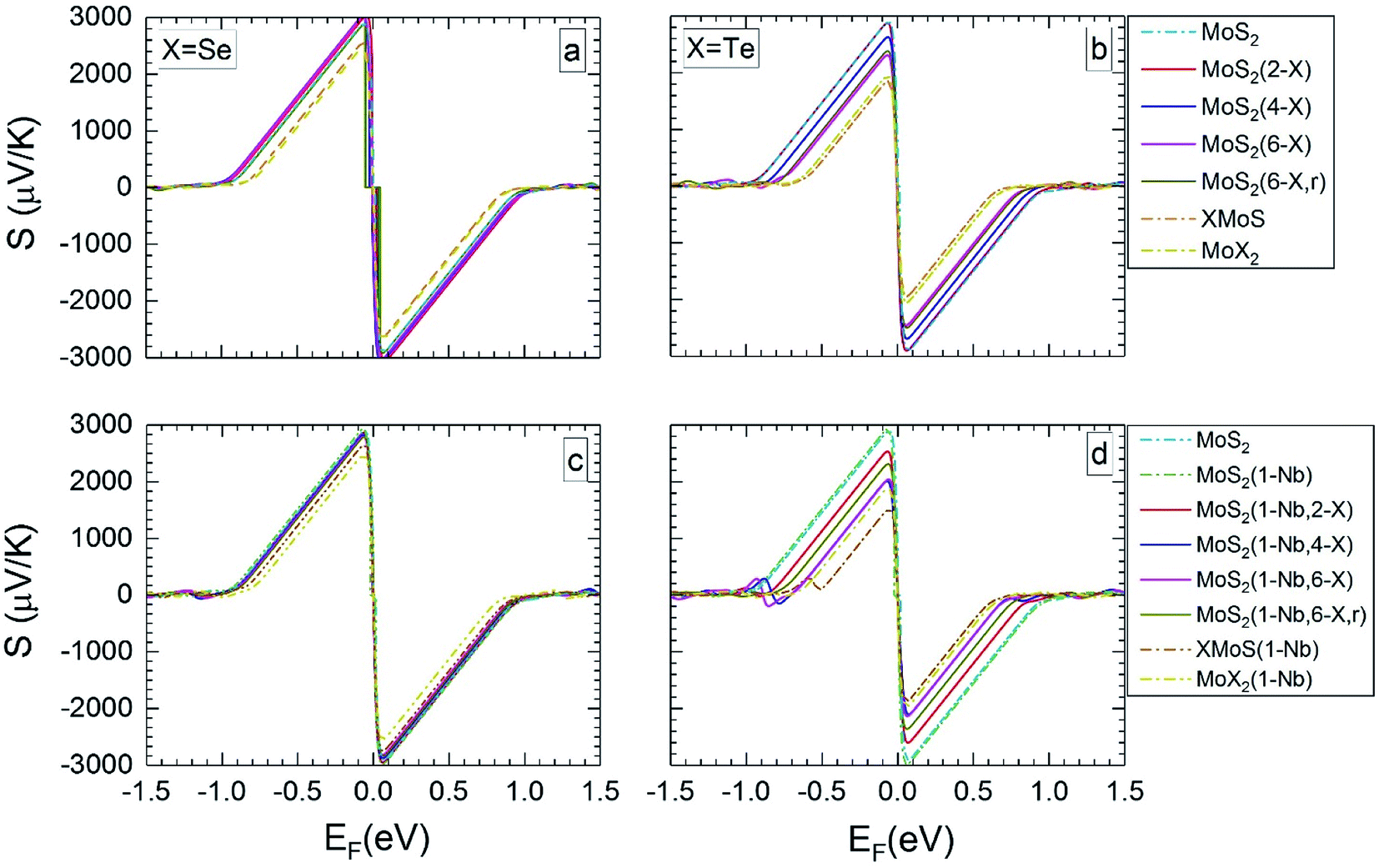 | ||
| Fig. 3 Seebeck coefficients at 300 K versus the Fermi level, for the different MLs, with X = Se or Te. | ||
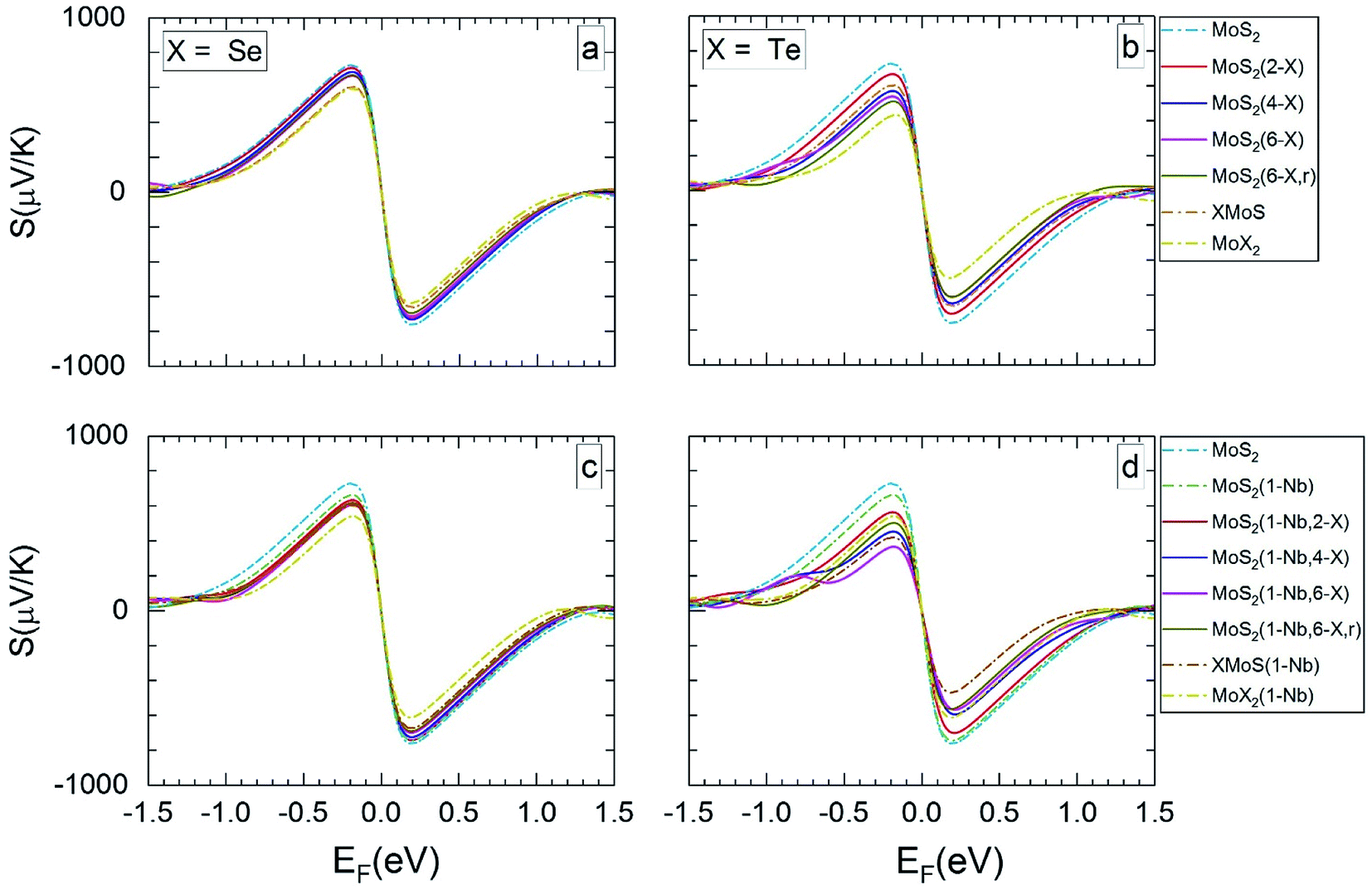 | ||
| Fig. 4 The calculated Seebeck coefficients at 1200 K vs. Fermi level, for the same MLs as presented in Fig. 3. | ||
For MLs with locally positioned Te atoms without (Fig. 3b and 4b) and with (Fig. 3d and 4d) Nb Smax (and Smin) decreases with increasing Te content. The lowest value of Smax (and Smin) is obtained for the TeMoS Janus layer and/or for MoTe2. The reduction with increasing Te content is still somewhat larger in case with the Nb. Reduction of Smax (and Smin) may be explained by the decrease of the bandgap (see Table 2). At 300 K the variation of the Seebeck coefficient of MoS2(1-Nb,6-Te,r) is slightly higher than MoS2(1-Nb,6-Te). This difference is more pronounced at 1200 K.
A direct comparison with literature data of the Seebeck coefficient is difficult. Hong et al.22 showed data of in-plane Seebeck data of the pristine MoS2 ML at 300 K. For a proper comparison, their energy scale was adopted to the band gap determined in the present work, and EF was set to zero at midgap (see above). A good agreement with our data is found. For example, our value of 1200 μV K−1 at EF = −0.60 eV (Fig. 3a) matches with 1200 μV K−1 obtained in ref. 22 at the corresponding Fermi level. A similar adoption or rescaling was used to compare with the in-plane Seebeck coefficient of Wickramaratne et al.36 for pristine MoS2 ML at 300 K. Also in this case our values match well with the literature data, e.g. at EF = −0.63 eV (Fig. 3a) with S = 1000 μV K−1.
Fig. 5 and 6 show ZT for the different MLs versus the Fermi level for temperatures of 300 and 1200 K, respectively. ZT results for 500 and 800 K can be found in Section SD of the ESI.†62 Like the Seebeck coefficient (Fig. 3 and 4) the TE figure of merit shows a significant dependence on the electrical doping, i.e. the Fermi level. In most cases, MoS2-based MLs modified by substitutional atoms show high ZT values of about 1 over a broader range of possible Fermi levels than Janus, MoSe2, and MoTe2 MLs.
 | ||
| Fig. 5 Thermoelectric figure of merit at 300 K in dependence on Fermi level, for the different MLs, with X = Se or Te. | ||
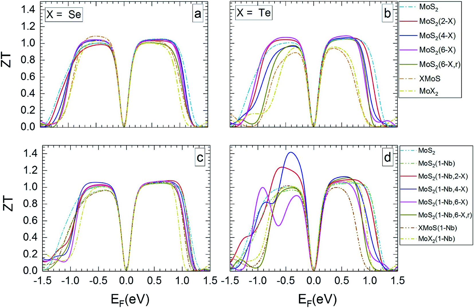 | ||
| Fig. 6 Thermoelectric figure of merit at 1200 K in dependence on Fermi level, for the MLs presented in Fig. 5. | ||
MLs with Se substitutional atoms (Fig. 5a and c) exhibit high ZT values in a wider region of Fermi-level values than in the case of Te substitutional atoms (Fig. 5b and d). Optimum ZT values are found for the Se substituted MLs with a Nb substitutional atom (Fig. 5c). In this case ZT is nearly constant in most of the possible n- or p-regions, with the exception of those close to mid gap and at band edges. In comparison with Fig. 5a, the Fermi-level range of high ZT value is slightly extended due to the Nb substitutional atom. Here, various p-doping levels may be possible between about −0.7 and −0.1 eV, or various n-doping levels between about 0.1 and 0.8 eV, with a value of the TE figure of merit close to 1. There is only a small difference between ZT data for random and local substitution of S by Se or Te. In some cases random substitution leads to a slightly smaller range of Fermi levels with high ZT values. The results depicted in Fig. 5a–d clearly show that SeMoS or TeMoS Janus layers as well as the MoSe2 and MoTe2 MLs do not perform better than the pristine MoS2 ML at 300 K. Replacing Mo by Nb locally leads to minor improvement of ZT of the Janus layers.
Our maximum value of ZT of about 1 for the pristine MoS2 ML at 300 K is in relatively good agreement with literature data of 0.97(1.35) for the p(n) region.36 Others authors obtained data that differ considerably: 0.47(0.22),56 0.51(0.23),65 and 0.25(0.68).13 This may be due to the different calculation schemes used in these publications.
The value of ZT slightly increases with temperature. At 1200 K (Fig. 6) the range of Fermi energies belonging to high ZT is somewhat narrower than at 300 K. In the case of MLs with substitutional Se atoms, as well as for the SeMoS Janus layer and the MoSe2 ML the temperature dependence of the main features is not very pronounced, as comparison of Fig. 5a and c with Fig. 6a and c shows. If the MLs contain Te substitutional atoms as well as in the case of the TeMoS Janus layer and the MoTe2 ML multiple peaks are found both at 300 and 1200 K. These features are also found at 500 and 800 K, see ESI,62 Fig. S6 and S7.† Multiple conduction channels due to multi-fold degenerate bands may explain the various peaks. Interestingly, MoS2(1-Nb,2-Te) and MoS2(1-Nb,4-Te) ML have the highest ZT value of 1.2 and 1.40, respectively at Fermi level of about −0.50 eV.
IV. Conclusions
Density functional theory and calculations using Boltzmann transport equations were employed to determine the electronic structure and the thermoelectric properties of various two-dimensional materials containing Mo, S, Nb, Se, and Te. In the MoS2-based MLs the substitution of S atoms by Te atoms (concentrations between 2.1 and 12.5 at%) leads to a stronger modification of the band structure than in the corresponding case with Se atoms. With increasing concentration of Se or Te the electronic structure becomes similar to that of the SeMoS or TeMoS Janus layers, and also similar to that of the MoSe2 or MoTe2 MLs. It was found that local and random introduction of substitutional Se or Te atoms yields not very different results. The substitution of Mo by Nb (concentration of 2.1 at%) does not alter the band structure significantly but leads to hole levels near the valence band maximum.The band structure data were used to calculate thermoelectric properties, in particular the Seebeck coefficient and the thermoelectric figure of merit. The two quantities were determined for different levels of p- or n-doping of the considered MLs and for different temperatures. The stronger influence of Te substitutional atoms on the band structure of MoS2-based MLs causes also more significant changes of the thermoelectric properties, compared to the pristine MoS2 ML. On the other hand, MLs with Se substitutional atoms show a high thermoelectric figure of merit in a broader range of possible p- or n-doping levels. In most cases investigated, the maximum thermoelectric figure of merit has a value of about one, both in p- and n-regions. This holds for temperatures between 300 and 1200 K, and not only for MoS2-based MLs with substitutional atoms but also for the Janus layers and for MoSe2 or MoTe2 MLs.
The comprehensive study performed in this work led to important data on properties of MoS2-based dichalcogenide MLs which had not yet been available. These results are very valuable for further experimental investigations as well as for the development and improvement of 2D materials.
Conflicts of interest
There are no conflicts to declare.Acknowledgements
Author M. Vallinayagam is grateful to the Center for Information Services and High Performance Computing (ZIH) at Technische Universität Dresden and to the Department of Information Service and Computing at Helmholtz-Zentrum Dresden-Rossendorf for providing extensive computing time.References
- G. J. Snyder and E. S. Toberer, Nat. Mater., 2008, 7, 105, DOI:10.1038/nmat2090.
- M. Dutta, T. Ghosh and K. Biswas, APL Mater., 2020, 8, 040910, DOI:10.1063/5.0002129.
- M. S. Dresselhaus, G. Chen, M. Y. Tang, R. G. Yang, H. Lee, D. Z. Wang, Z. F. Ren, J. P. Fleurial and P. Gogna, Adv. Mater., 2007, 19, 1043, DOI:10.1002/adma.200600527.
- D. D. Fan, H. J. Liu, L. Cheng, P. H. Jiang, J. Shi and X. F. Tang, Appl. Phys. Lett., 2014, 105, 133113, DOI:10.1063/1.4897349.
- L. D. Hicks and M. S. Dresselhaus, Phys. Rev. B: Condens. Matter Mater. Phys., 1993, 47, 12727, DOI:10.1103/physrevb.47.12727.
- J. R. Szczech, J. M. Higgins and S. Jin, J. Mater. Chem., 2011, 21, 4037, 10.1039/c0jm02755c.
- P. A. Erdman, F. Mazza, R. Bosisio, G. Benenti, R. Fazio and F. Taddei, Phys. Rev. B, 2017, 95, 245432, DOI:10.1103/PhysRevB.95.245432.
- P. Yan, G. Gao, G. Ding and D. Qin, RSC Adv., 2019, 9, 12394, 10.1039/c9ra00586b.
- J. P. Heremans, V. Jovovic, E. S. Toberer, A. Saramat, K. Kurosaki, A. Charoenphakdee, S. Yamanaka and G. J. Snyde, Science, 2008, 321, 554, DOI:10.1126/science.1159725.
- Y. Wang, N. Xu, D. Li and J. Zhu, Adv. Funct. Mater., 2017, 27, 1604134, DOI:10.1002/adfm.201604134.
- Z. Zhang, Y. Xie, Y. Ouyang and Y. Chen, Int. J. Heat Mass Transfer, 2017, 108, 417, DOI:10.1016/j.ijheatmasstransfer.2016.12.041.
- A. Shafique and Y. H. Shin, Sci. Rep., 2017, 7, 506, DOI:10.1038/s41598-017-00598-7.
- W. Huang, X. Luo, C. K. Gan, S. Y. Quek and G. Liang, Phys. Chem. Chem. Phys., 2014, 16, 10866–10874, 10.1039/c4cp00487f.
- M. Chhowalla, H. S. Shin, G. Eda, L. J. Li, K. P. Loh and H. Zhang, Nat. Chem., 2013, 5, 263, DOI:10.1038/nchem.1589.
- Q. Feng, Y. Zhu, J. Hong, M. Zhang, W. Duan, N. Mao, J. Wu, H. Xu, F. Dong, F. Lin, C. Jin, C. Wang, J. Zhang and L. Xie, Adv. Mater., 2014, 26, 2648, DOI:10.1002/adma.201306095.
- H. P. Komsa and A. V. Krasheninnikov, J. Phys. Chem. Lett., 2012, 3, 3652, DOI:10.1021/jz301673x.
- M. R. Laskar, D. N. Nath, L. Ma, E. W. Lee, C. H. Lee, T. Kent, Z. Yang, R. Mishra, M. A. Roldan, J.-C. Idrobo, S. T. Pantelides, S. J. Pennycook, R. C. Myers, Y. Wu and S. Rajan, Appl. Phys. Lett., 2014, 104, 092104, DOI:10.1063/1.4867197.
- H. Li, Q. Zhang, X. Duan, X. Wu, X. Fan, X. Zhu, X. Zhuang, W. Hu, H. Zhou, A. Pan and X. Duan, J. Am. Chem. Soc., 2015, 137, 5284, DOI:10.1021/jacs.5b01594.
- S. Tongay, D. S. Narang, J. Kang, W. Fan, C. Ko, A. V. Luce, K. X. Wang, J. Suh, K. D. Patel, V. M. Pathak, J. Li and J. Wu, Appl. Phys. Lett., 2014, 104, 012101, DOI:10.1063/1.4834358.
- S. Kumar and U. Schwingenschlögl, Chem. Mater., 2015, 27, 1278, DOI:10.1021/cm504244b.
- C. Lee, J. Hong, M. H. Whangbo and J. H. Shim, Chem. Mater., 2013, 25, 3745, DOI:10.1021/cm402281n.
- J. Hong, C. Lee, J. S. Park and J. H. Shim, Phys. Rev. B, 2016, 93, 035445, DOI:10.1103/PhysRevB.93.035445.
- M. Sharma, A. Kumar, P. K. Ahluwalia and R. Pandey, J. Appl. Phys., 2014, 116, 063711, DOI:10.1063/1.4892798.
- H. Li, Q. Zhang, X. Duan, X. Wu, X. Fan, X. Zhu, X. Zhuang, W. Hu, H. Zhou, A. Pan and X. Duan, J. Am. Chem. Soc., 2015, 349, 524, DOI:10.1126/science.aab4097.
- S. D. Guo, Comput. Mater. Sci., 2016, 123, 8, DOI:10.1016/j.commatsci.2016.06.011.
- H. Peelaers and C. G. Van de Walle, Phys. Rev. B: Condens. Matter Mater. Phys., 2012, 86, 241401, DOI:10.1103/PhysRevB.86.241401.
- C. Ataca, H. Şahin and S. Ciraci, J. Phys. Chem. C, 2012, 116, 8983, DOI:10.1021/jp212558p.
- T. Böker, R. Severin, A. Müller, C. Janowitz, R. Manzke, D. Voß, P. Krüger, A. Mazur and J. Pollmann, Phys. Rev. B: Condens. Matter Mater. Phys., 2001, 64, 235305, DOI:10.1103/PhysRevB.64.235305.
- S. Lebègue, T. Björkman, M. Klintenberg, R. M. Nieminen and O. Eriksson, Phys. Rev. X, 2013, 3, 031002, DOI:10.1103/PhysRevX.3.031002.
- G. B. Liu, D. Xiao, Y. Yao, X. Xu and W. Yao, Chem. Soc. Rev., 2015, 44, 2643, 10.1039/c4cs00301b.
- W. Zhao, Z. Ghorannevis, L. Chu, M. Toh, C. Kloc, P. H. Tan and G. Eda, ACS Nano, 2011, 7, 791, DOI:10.1021/nn305275h.
- Q. H. Wang, K. Kalantar-Zadeh, A. Kis, J. N. Coleman and M. S. Strano, Nat. Nanotechnol., 2012, 7, 699, DOI:10.1038/nnano.2012.193.
- M. Acerce, D. Voiry and M. Chhowalla, Nat. Nanotechnol., 2015, 10, 313, DOI:10.1038/nnano.2015.40.
- B. Radisavljevic, A. Radenovic, J. Brivio, V. Giacometti and A. Kis, Nat. Nanotechnol., 2011, 6, 147, DOI:10.1038/nnano.2010.279.
- C. Ataca, M. Topsakal, E. Aktürk and S. Ciraci, J. Phys. Chem. C, 2011, 115, 16354, DOI:10.1021/jp205116x.
- D. Wickramaratne, F. Zahid and R. K. Lake, J. Chem. Phys., 2014, 140, 124710, DOI:10.1063/1.4869142.
- Q. Feng, N. Mao, J. Wu, H. Xu, C. Wang, J. Zhang and L. Xie, ACS Nano, 2015, 9, 7450, DOI:10.1021/acsnano.5b02506.
- J. Mann, Q. Ma, P. M. Odenthal, M. Isarraraz, D. Le, E. Preciado, D. Barroso, K. Yamaguchi, G. von Son Palacio, A. Nguyen, T. Tran, M. Wurch, A. Nguyen, V. Klee, S. Bobek, D. Sun, T. F. Heinz, T. S. Rahman, R. Kawakami and L. Bartels, Adv. Mater., 2014, 26, 1399–1404, DOI:10.1002/adma.201304389.
- J. Kang, S. Tongay, J. Li and J. Wu, J. Appl. Phys., 2013, 113, 143703, DOI:10.1063/1.4799126.
- A. Y. Lu, H. Zhu, J. Xiao, C. P. Chuu, Y. Han, M. H. Chiu, C. C. Cheng, C. W. Yang, K. H. Wei, Y. Yang, Y. Wang, D. Sokaras, D. Nordlund, P. Yang, D. A. Muller, M. Y. Chou, X. Zhang and L. J. Li, Nat. Nanotechnol., 2017, 12, 744, DOI:10.1038/nnano.2017.100.
- L. Dong, J. Lou and V. B. Shenoy, ACS Nano, 2017, 11, 8242, DOI:10.1021/acsnano.7b03313.
- S. D. Guo, X. S. Guo and Y. Deng, J. Appl. Phys., 2019, 126, 154301, DOI:10.1063/1.5124677.
- S. D. Guo and J. Dong, Semicond. Sci. Technol., 2018, 33, 085003, DOI:10.1088/1361-6641/aacb11.
- Y. Gong, Z. Liu, A. R. Lupini, G. Shi, J. Lin, S. Najmaei, Z. Lin, A. L. Elias, A. Berkdemir, G. You, H. Terrones, M. Terrones, R. Vajtai, S. T. Pantelides, S. J. Pennycook, J. Lou, W. Zhou and P. M. Ajayan, Nano Lett., 2014, 14, 442, DOI:10.1021/nl4032296.
- J. Suh, T. E. Park, D. Y. Lin, D. Fu, J. Park, H. J. Jung, Y. Chen, C. Ko, C. Jang, Y. Sun, R. Sinclair, J. Chang, S. Tongay and J. Wu, Nano Lett., 2014, 14, 6976, DOI:10.1021/nl503251h.
- K. Momma and F. Izumi, J. Appl. Crystallogr., 2011, 44, 1272, DOI:10.1107/s0021889811038970.
- G. Kresse and J. Furthmiiller, Comput. Mater. Sci., 1996, 6, 15, DOI:10.1016/0927-0256(96)00008-0.
- P. E. Blochl, Phys. Rev. B: Condens. Matter Mater. Phys., 1994, 50, 17953, DOI:10.1103/physrevb.50.17953.
- H. J. Monkhorst and J. D. Pack, Phys. Rev. B: Solid State, 1976, 13, 5188, DOI:10.1103/PhysRevB.13.5188.
- P. E. Blochl, O. Jepsen and O. K. Andersen, Phys. Rev. B: Condens. Matter Mater. Phys., 1994, 49, 16223, DOI:10.1103/physrevb.49.16223.
- G. K. H. Madsen and D. J. Singh, Comput. Phys. Commun., 2006, 175, 67, DOI:10.1016/j.cpc.2006.03.007.
- S. K. Mahatha, K. D. Patel and K. S. Menon, J. Phys.: Condens. Matter, 2012, 24, 475504, DOI:10.1088/0953-8984/24/47/475504.
- L. Liang and V. Meunier, Nanoscale, 2014, 6, 5394, 10.1039/c3nr06906k.
- V. V. Ivanovskaya, A. Zobelli, A. Gloter, N. Brun, V. Serin and C. Colliex, Phys. Rev. B: Condens. Matter Mater. Phys., 2008, 78, 134104, DOI:10.1103/PhysRevB.78.134104.
- A. Molina-Sánchez and L. Wirtz, Phys. Rev. B: Condens. Matter Mater. Phys., 2011, 84, 155413, DOI:10.1103/PhysRevB.84.155413.
- G. Özbal, R. T. Senger, C. Sevik and H. Sevinçli, Phys. Rev. B, 2019, 100, 085415, DOI:10.1103/PhysRevB.100.085415.
- K. K. Kam and B. A. Parkinson, J. Phys. Chem., 1982, 86, 463, DOI:10.1021/j100393a010.
- K. Dolui, I. Rungger, C. Das Pemmaraju and S. Sanvito, Phys. Rev. B: Condens. Matter Mater. Phys., 2013, 88, 075420, DOI:10.1103/PhysRevB.88.075420.
- Z. Wang, J. Mater. Chem. C, 2018, 6, 13000, 10.1039/c8tc04951c.
- C. Ruppert, O. B. Aslan and T. F. Heinz, Nano Lett., 2014, 14, 6231, DOI:10.1021/nl502557g.
- S. H. Su, Y. T. Hsu, Y. H. Chang, M. H. Chiu, C. L. Hsu, W. T. Hsu, W. H. Chang, J. H. He and L. J. Li, Small, 2014, 10, 2589, DOI:10.1002/smll.201302893.
- See the ESI† for Results and discussion on formation energy and density of states.
- Y. Cai, J. Lan, G. Zhang and Y.-W. Zhang, Phys. Rev. B: Condens. Matter Mater. Phys., 2014, 89, 035438, DOI:10.1103/PhysRevB.89.035438.
- A. Shafique and Y. H. Shin, Phys. Chem. Chem. Phys., 2017, 19, 32072, 10.1039/c7cp06065c.
- W. Huang, H. Da and G. Liang, J. Appl. Phys., 2013, 113, 104304, DOI:10.1063/1.4794363.
Footnote |
| † Electronic supplementary information (ESI) available. See DOI: 10.1039/d0ra08463h |
| This journal is © The Royal Society of Chemistry 2020 |