
 Open Access Article
 This Open Access Article is licensed under a Creative Commons Attribution-Non Commercial 3.0 Unported Licence
Spin–orbit coupling effect on electronic, optical, and thermoelectric properties of Janus Ga2SSe
Hong T. T. Nguyenab,
Vo T. T. Vicd,
Tuan V. Vu ab,
Nguyen V. Hieu*e,
Dung V. Lu*e,
D. P. Raif and
Nguyen T. T. Binhgh
ab,
Nguyen V. Hieu*e,
Dung V. Lu*e,
D. P. Raif and
Nguyen T. T. Binhgh
aDivision of Computational Physics, Institute for Computational Science, Ton Duc Thang University, Ho Chi Minh City, Vietnam. E-mail: nguyenthithamhong@tdtu.edu.vn; vuvantuan@tdtu.edu.vn
bFaculty of Electrical & Electronics Engineering, Ton Duc Thang University, Ho Chi Minh City, Vietnam
cDepartment of Physics, University of Education, Hue University, Hue, Vietnam
dDepartment of Fundamental Sciences, University of Medicine and Pharmacy, Hue University, Hue, Vietnam
eFaculty of Physics, The University of Danang – University of Science and Education, Da Nang, Vietnam. E-mail: nvhieu@ued.udn.vn; dvlu@ued.udn.vn
fDepartment of Physics, Physical Sciences Research Center, Pachhunga University College, Aizawl 796001, India
gInstitute of Research and Development, Duy Tan University, Da Nang 550000, Vietnam. E-mail: nguyentthanhbinh8@duytan.edu.vn
hFaculty of Natural Sciences, Duy Tan University, Da Nang 550000, Vietnam
First published on 17th December 2020
Abstract
In this paper, we investigate the electronic, optical, and thermoelectric properties of Ga2SSe monolayer by using density functional theory. Via analysis of the phonon spectrum and ab initio molecular dynamics simulations, Ga2SSe is confirmed to be stable at room temperature. Our calculations demonstrate that Ga2SSe exhibits indirect semiconductor characteristics and the spin–orbit coupling (SOC) effect has slightly reduced its band gap. Besides, the band gap of Ga2SSe depends tightly on the biaxial strain. When the SOC effect is included, small spin–orbit splitting energy of 90 meV has been found in the valence band. However, the spin–orbit splitting energy dramatically changes in the presence of biaxial strain. Ga2SSe exhibits high optical absorption intensity in the near-ultraviolet region, up to 8.444 × 104 cm−1, which is needed for applications in optoelectronic devices. By using the Boltzmann transport equations, the electronic transport coefficients of Ga2SSe are comprehensively investigated. Our calculations reveal that Ga2SSe exhibits a very low lattice thermal conductivity and high figure of merit ZT and we can enhance its ZT by temperature. Our findings provide further insight into the physical properties of Ga2SSe as well as point to prospects for its application in next-generation high-performance devices.
1 Introduction
The physical properties of two-dimensional (2D) materials are very sensitive to the perfection of the atomic structure.1–3 The breaking of symmetrical structures in 2D materials can offer new physical properties with many potentials for applications in technology. Motivated by this view, the Janus asymmetric structure MoSSe has been experimentally reported recently.4,5 Compared with MoS2 or MoSe2, there is a lack of mirror symmetry in the Janus structure MoSSe and out-of-plane structural asymmetry in MoSSe has been identified by spectroscopy.4 The successful synthesis of Janus MoSSe opened a new chapter in the research for the 2D family and many different types of Janus structures were theoretically studied recently.6–9Janus structures show a high prospect for use as thermoelectric materials due to their owning a high thermoelectric figure of merit.10 With suitable band edge alignment, Janus structures are expected to be used in photocatalytic water splitting.11 By using density functional theory (DFT) calculations, Yao and co-workers have revealed that mirror symmetry breaking in Janus MoSSe structure induces a very large Rashba spin splitting.12 Also, one can modulate the electronic properties of Janus monolayers by an applied strain13 or external electric field.14 Recent DFT calculations demonstrated that MoSeTe possesses high absorption intensity and becoming a great candidate for applications in optoelectronic devices.15 Recently, van der Waals heterostructures based Janus monolayers have been studied with a lot of attention.7,16,17 In graphene/Ga2SSe heterostructures, a small band gap has been found in graphene due to weak interactions between graphene and Ga2SSe.17 It implies that forming heterostructures with the Janus structure is one of the ways to overcome the gapless disadvantage of graphene.
Excited by the successes in studies of Janus dichalcogenides, Janus monochalcogenides structures, especially Janus structures based on group III–VI compounds, have gained attention recently.11,18 Wan and co-workers indicated that the Janus In2SeTe exhibits higher carrier mobility that of InSe.19 Also, strain engineering is one of the good ways to modulate the thermal conductivity of InSe-based Janus.19 Using DFT calculations, Gou et al. have shown that the Janus group III monochalcogenides possess a high piezoelectric coefficient, and additional out of plane piezoelectric coefficients were found in Janus group III monochalcogenides due to induces out of plane dipolar polarization caused by breaking mirror symmetry.20 In this work, we systematically investigate the effect of spin–orbit coupling (SOC) on the electronic, optical, and thermoelectric properties of Janus Ga2SSe monolayer by mean of DFT calculations. We focus on the influence of SOC on the band structure and band gap of Ga2SSe. Optical characteristics and electronic transport coefficients are calculated and discussed in detail when the SOC was included.
2 Computational details
The projector augmented wave method is used within the DFT calculations as implemented in the Quantum ESPRESSO code.21 The Perdew–Burke–Ernzerhof (PBE) functional22 with the spin–orbit coupling (SOC)23 of the generalized gradient approximation (GGA) is used to consider the interaction of the exchange-correlation. A 15 × 15 × 1 k-point mesh in the Brillouin zone is used for optimization. A vacuum space in the c direction was set to be 20 Å to avoid any artificial interactions between neighbor plates. All self-consistent calculations and geometric optimization are completed until the difference in energy between the forces on each atom and the electron steps converge to be 10−3 eV Å−1 and 10−6 eV, respectively.A large supercell of 4 × 4 × 1 is used for the calculations of the phonon spectrum to obtain more accurate results. The thermal stability is tested by the ab initio molecular dynamics (AIMD) simulations24 performing through the Nose-thermostat algorithm. Both PBE and PBE + SOC methods are used to study the thermoelectric properties. A 90 × 90 × 1 k-point mesh is used for calculations of the electronic transport properties. The canonical ensemble (NVT) with constant temperature is used for the calculations of the thermoelectric properties. The electronic transport coefficients are estimated by using the semi-classical Boltzmann transport theory within the constant scattering time and rigid band approximations as performed in the BoltzTrap.25 The Phono3py package26 has been used to calculate the lattice thermal conductivity.
3 Results and discussion
By replacing one chalcogen atom by another, we can build the Janus Ga2SSe monolayer from either GaS or GaSe. While both GaS and GaSe belong to the P![[6 with combining macron]](https://www.rsc.org/images/entities/char_0036_0304.gif) m2 (D3h) space group with mirror symmetry, the lattice of Ga2SSe has the P3m1 (C3v) crystal symmetry. The absence of mirror symmetry in the geometrical structure of Ga2SSe is expected to give it many novel properties that do not exist in pure monochalcogenides GaSe or GaS. In Fig. 1(a), we show the geometrical structure of Ga2SSe monolayer at equilibrium. Our calculations revealed that the lattice constant of Ga2SSe after full relaxation is a = 3.728 Å, which is larger/smaller than that of GaS/GaSe. The lacking of out-plane mirror symmetry in Janus Ga2SSe is due to the difference between Ga–S and Ga–Se bond lengths. Ga–S and Ga–Se bond lengths are respectively 2.387 Å and 2.472 Å. Structural parameters, such as the lattice constant or the bond length, of a material depend on the size of the elements in the material. The difference in the lattice constants between Janus structure Ga2SSe and pure monochalcogenides GaS and GaSe is due to the difference in the size of the chalcogen atom in these compounds. The structural parameters of Ga2SSe are listed in Table 1.
m2 (D3h) space group with mirror symmetry, the lattice of Ga2SSe has the P3m1 (C3v) crystal symmetry. The absence of mirror symmetry in the geometrical structure of Ga2SSe is expected to give it many novel properties that do not exist in pure monochalcogenides GaSe or GaS. In Fig. 1(a), we show the geometrical structure of Ga2SSe monolayer at equilibrium. Our calculations revealed that the lattice constant of Ga2SSe after full relaxation is a = 3.728 Å, which is larger/smaller than that of GaS/GaSe. The lacking of out-plane mirror symmetry in Janus Ga2SSe is due to the difference between Ga–S and Ga–Se bond lengths. Ga–S and Ga–Se bond lengths are respectively 2.387 Å and 2.472 Å. Structural parameters, such as the lattice constant or the bond length, of a material depend on the size of the elements in the material. The difference in the lattice constants between Janus structure Ga2SSe and pure monochalcogenides GaS and GaSe is due to the difference in the size of the chalcogen atom in these compounds. The structural parameters of Ga2SSe are listed in Table 1.
 | ||
| Fig. 1 (a) Geometric structure, (b) phonon dispersion, and (c) time-dependent AIMD simulations of temperature fluctuation at room temperature of Ga2SSe monolayer. Insets in (c) are the atomic structures of Ga2SSe before and after heat-treatment of 5 ps. | ||
| a (Å) | dGa–S (Å) | dGa–Se (Å) | dGa–Ga (Å) | h (Å) | ϕ∠SGaGa (deg.) | ϕ∠GaGaSe (deg.) | |
|---|---|---|---|---|---|---|---|
| GaS | 3.585 | 2.471 | — | 2.457 | 4.651 | 117.375 | — |
| GaSe | 3.818 | — | 2.497 | 2.468 | 4.814 | — | 117.965 |
| Ga2SSe | 3.728 | 2.387 | 2.472 | 2.465 | 4.725 | 115.762 | 119.637 |
The structural stability of material can be attested through an analysis of its phonon dispersion relations. The structure is dynamically stable when its phonon modes throughout the Brillouin zone have a positive frequency. The restoring force, which counteracts the displacement of atoms, is lost if there are negative frequencies in the phonon spectrum. The phonon dispersion relations of Ga2SSe monolayer is shown in Fig. 1(b). We can see that there are 12 vibrational branches in the phonon spectrum of Ga2SSe. Three optical branches are the longitudinal, transverse, and flexural branches. There is an intersection between the optical branches and the acoustic branches. There are nine optical modes, including three nondegenerate modes and three doubly degenerate at the Γ-point. Most importantly, no soft modes are found in the phonon dispersion curves of Ga2SSe. This confirms that Ga2SSe is dynamically stable and we can synthesize Ga2SSe as a free-standing monolayer.
While dynamical stability is a guarantee for a material to be physically viable, thermal stability is a necessary condition for that material to be applied in real equipment. To test the thermal stability, the time-dependence of the temperature fluctuation of Ga2SSe is calculated by AIMD simulations and the obtained result is presented in Fig. 1(c). Our calculated results demonstrated that there is no significant distortion in the atomic structure of Ga2SSe after 5 ps (with 5000 time-steps) of heat-treatment at room temperature. There is no bond-breaking as well as no structural reconstruction in Ga2SSe after heating, warranting its thermal stability.
In Fig. 2, we show our calculated results for band structure, which is plotted along the Γ–M–K–Γ direction, and partial density of states (PDOS) of Ga2SSe at equilibrium using both PBE and PBE-SOC methods. From Fig. 2(a), we can see that the Janus Ga2SSe is an indirect semiconductor with the conduction band minimum (CBM) and valence band maximum (VBM) locating respectively at M-point and on MK-path. At the PBE level, the indirect band gap of Ga2SSe is EgK→MK = 2.070 eV. However, the direct band gap by PBE functional is very close to the indirect one, EgK→MK = 2.183 eV, as depicted in Fig. 2(a). This implies that the change of position of the VBM can take place when the Janus monolayer is influenced by external factors such as strain engineering or external electric field.
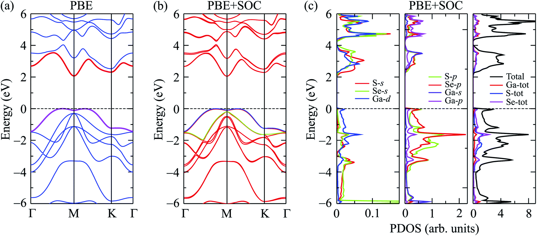 | ||
| Fig. 2 Calculated band structures of Ga2SSe by PBE (a) and PBE + SOC (b) methods. (c) PDOS of Ga2SSe by PBE + SOC method. | ||
It is well-known that the SOC effect plays a key role in determining the electronic properties of materials, especially in the case of compounds containing heavy elements. The heavier the element-containing material, the greater the influence of the SOC on the electronic properties of that material. When the SOC effect was included, the band structure was significantly altered as shown in Fig. 2(b). By comparing Fig. 2(a) and (b), we can see that there are splitting bands in the band structure of Ga2SSe due to the spin–orbit coupling. Our calculations revealed that the SOC effect slightly reduced the band gap of Ga2SSe, from 2.070 eV (without SOC) to 2.050 eV (with SOC). Also, small spin–orbit splitting energy of Δ = 90 meV is found in the valence band at the M-point in the Brillouin zone. Due to the size of elements, the spin–orbit splitting energy Δ in Ga2SSe is smaller than that in other compounds in the same group III such as Ga2SeTe (416 meV).9 This difference in spin–orbit splitting energy is due to the difference in size between the S and Te elements. In Fig. 2(c), we show our calculations for the partial density of states (DOS) of Ga2SSe by PBE + SOC method. Based on the analysis of the PDOS, we can estimate the contribution of the atom orbital to the electronic bands of Ga2SSe. We can see that the S-p and Se-p orbitals have a great contribution to the valence band. For the atom orbitals of Ga, the Ga-s orbital has a dominant contribution to the conduction band while the valence band receives significant contributions from the Ga-p orbital. In Fig. 3, we plot the weighted band structure of Ga2SSe, which can help to estimate the contribution of atomic orbital to the CBM and VBM. We show only the s- and p-orbitals of the atoms because the d-orbital contributes to the higher energy region. From Fig. 3, we can see that the VBM is largely contributed from the S-d and Se-d orbitals while the Ga-s and S-s orbitals significantly contribute to the CBM.
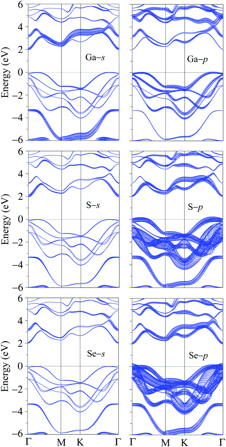 | ||
| Fig. 3 Weighted band structures of Ga2SSe monolayer. | ||
Electronic bands of 2D materials are sensitive to the change in geometrical structure. Therefore, strain engineering is one of the best ways to drive the electronic properties of 2D materials. The band structure of Ga2SSe under different values of biaxial strain εb is shown in Fig. 4. The band structure of Ga2SSe changes interestingly in the presence of strain. When compressive strain is applied, the band structure of Ga2SSe changes perfectly as shown in Fig. 4(a). The VBM tends to shift to the M-point of the Brillouin zone. At the same time, the CBM tends to shift away from the M-point and towards the K-point. The consequence of this is that Ga2SSe remains an indirect semiconductor under the compressive strain even though the VBM moves to the M-point when εb = −3%. The influence of the tensile strain εb > 0) on the band structure of Ga2SSe is depicted in Fig. 4(b). From Fig. 4(b), we can see that Ga2SSe is still the indirect semiconductor in the whole tensile strain range with the CBM and VBM located at M-point and MK-path, respectively. However, the band gap of Ga2SSe decreases significantly with increasing tensile strain. The band gap of Ga2SSe decreases almost linearly with increasing tensile strain as shown in Fig. 5(a). Meanwhile, the compressive strain not only significantly changed the band structure of Ga2SSe as above-mentioned, but also changed its band gap irregularly. In the presence of the compressive strain, the band gap increases to the maximum value at εb = 3% and then decreases again with a continued increase in compressive strain. More interestingly, while the difference in band gap calculated by PBE and PBE + SOC methods is quite small in the case of tensile strain, there is a clear difference between them in the case of compressive strain, especially in large compressive strain. The maximum value of the calculated band gap by PBE and PBE + SOC methods is 2.488 eV and 2.376 eV, respectively. In Fig. 5(b), we depict the biaxial strain dependence of spin–orbit splitting energy Δ. As above-mentioned, the spin–orbit splitting energy Δ in Ga2SSe is quite small at equilibrium (only 90 meV), however, Δ decreases rapidly with the increasing of the tensile strain. The spin–orbit splitting energy is up to 419 meV at εb = 7%. On the other hand, the spin–orbit splitting energy depends dramatically on the compressive strain. When the compressive strain strength increases, the splitting energy Δ decreases to 12 meV at εb = −1% and then increases again. It is clear that the structural strain has drastically changed the electronic structure of the Janus Ga2SSe, not only the band gap but also the spin–orbit splitting energy.
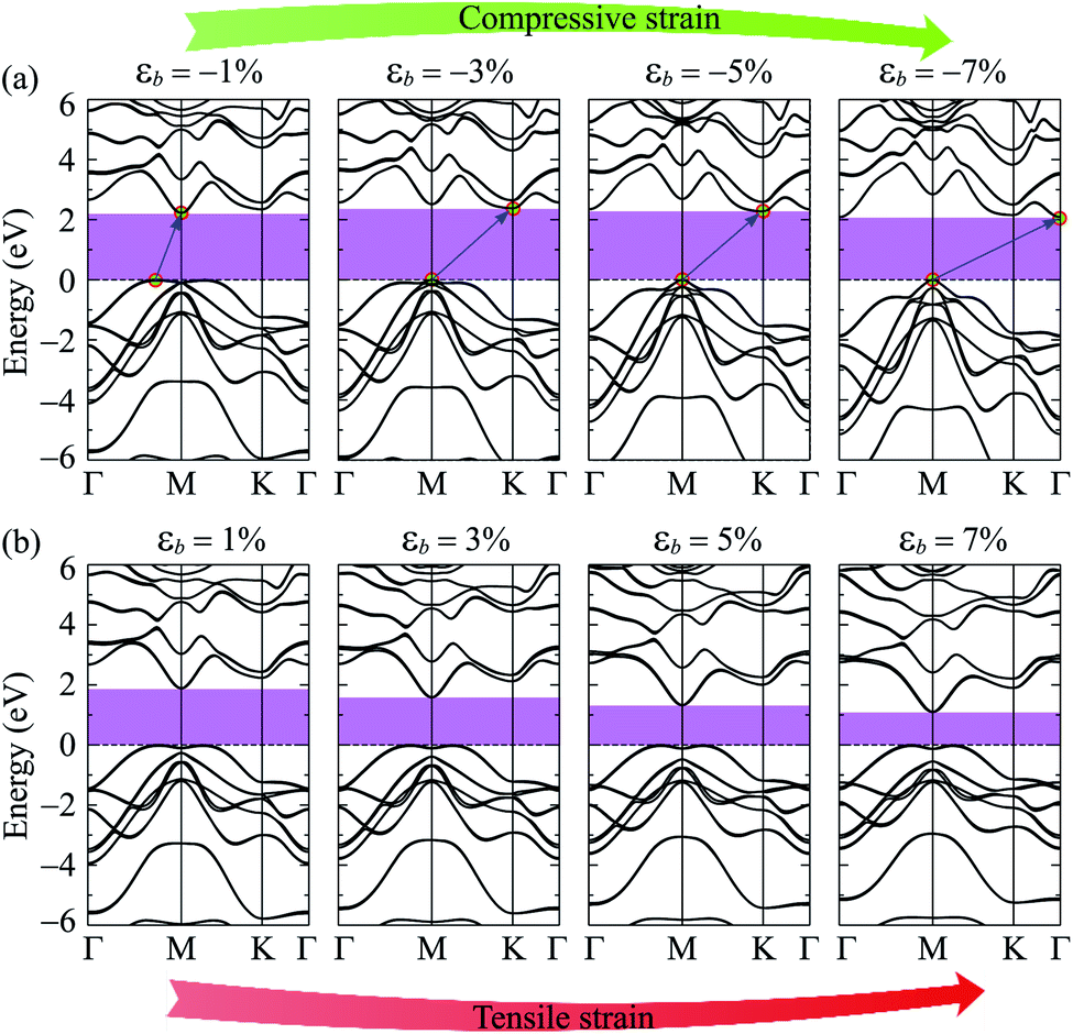 | ||
| Fig. 4 Band structure of Ga2SSe under the compressive (a) and tensile (b) strains. | ||
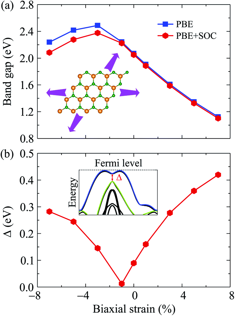 | ||
| Fig. 5 Band gap (a) and spin–orbit splitting energy Δ (b) of Ga2SSe as a function of biaxial strain. | ||
We next study the optical properties of the Janus Ga2SSe. The incoming photon is parallel polarized and a large range of photon energy ℏω from 0 eV to 12 eV is investigated in this work. The fundamental optical characteristics can be studied through the dielectric function as ε(ω) = ε1(ω) + iε2(ω). The imaginary part ε2(ω) is usually calculated first by summing of the filled–unfilled state transitions:27,28
 | (1) |
 | (2) |
The optical absorption coefficient A(ω) can be derived from the parts of ε(ω) as the follows:29
 | (3) |
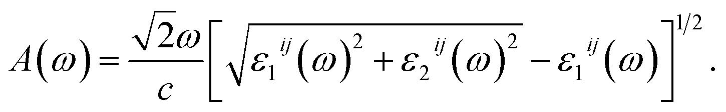
The calculated dielectric function by the PBE + SOC method is presented in Fig. 6(a). We can see that Ga2SSe exhibits low static dielectric constant ε1(0). At equilibrium, Ga2SSe has ε1(0) = 3.209, which is lower than that of Ga2STe30 or Ga2SeTe.9 This is consistent with Penn model,31 which claims that static dielectric constant is inversely proportional to direct bandgap of materials. The optical characteristics is strongly connected to the ε2(ω), which is also presented in Fig. 6(a). As shown in Fig. 6(a), it is found that the first peak in ε2(ω) spectrum is located at the incoming light energy ℏω = 4.313 eV. The main peak in ε2(ω) is also located in the near-ultraviolet region, at ℏω = 4.640 eV. These optical peaks are related to the optical absorbance peaks, which are shown in Fig. 6(b). Optical absorption in Ga2SSe is activated in the visible light region (at ℏω ≈ 2 eV) then absorption intensity rapidly increases. The maximum intensity in the visible region is up to 1.2 × 104 cm−1. The first absorption peak is at ℏω = 5.102 eV in the near-ultraviolet region. Ga2SSe exhibits great absorption intensity in the near-ultraviolet region. The maximum absorption intensity is up to A(ω) = 8.444 × 104 cm−1 at ℏω = 7.334 eV.
 | ||
| Fig. 6 (a) Calculated the dielectric function and (b) optical absorption coefficient of Ga2SSe monolayer by PBE + SOC method. | ||
In the last part of this work, we consider the electronic transport coefficients of Ga2SSe monolayer. Previously, Hicks and Dresselhaus have indicated that low-dimensional nanostructures can be thermoelectric materials.32 We focus on the basic electronic transport coefficients, including the Seebeck coefficient S, electrical conductivity σ, power factor S2σ, and figure of merit ZT, which are all calculated by PBE + SOC method.
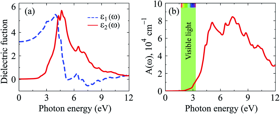
The relaxation time τ is a key parameter of the electronic transport features. The τ depends highly on the scattering processes in the materials. Hence, we assume that τ does not dependent on the doping level N. In the present work, the EPW package33 interfaced with Quantum ESPRESSO21 is used to estimate the relaxation time. Obtained results demonstrate that the relaxation time of Ga2SSe at room temperature (T = 300 K) is 3.63 × 10⁻¹⁴ s. This value is close to the previous report for MoS2 being 5.17 × 10⁻¹⁴ s.34 The dependence of the relaxation time on temperature T is shown in Fig. 7. From Fig. 7, it is revealed that the smaller the relaxation time in the higher the temperature region.
 | ||
| Fig. 7 Calculated temperature-dependent relaxation time of Ga2SSe monolayer by PBE + SOC method. | ||
Based on the electronic band structures, the electronic transport coefficients have been calculated by using the Boltzmann transport equation within the constant scattering time approximation via the BoltzTraP package.25 The electronic transport properties can be built from the transport distribution Ξ, which can be obtained from the band structure of material35
 | (4) |
![[v with combining right harpoon above (vector)]](https://www.rsc.org/images/entities/i_char_0076_20d1.gif) α/β stands for the group velocity of the carrier with the wavevector
α/β stands for the group velocity of the carrier with the wavevector ![[k with combining right harpoon above (vector)]](https://www.rsc.org/images/entities/i_char_006b_20d1.gif) and τ is the carrier relaxation time. The electrical conductivity σ, electronic thermal conductivity κe, and the Seebeck coefficient S are given by35
and τ is the carrier relaxation time. The electrical conductivity σ, electronic thermal conductivity κe, and the Seebeck coefficient S are given by35
 | (5) |
 | (6) |
 | (7) |
In the nanostructures, the number of holes/electrons per unit cell or the doping level N has been used instead of doping concentration. The positive/negative value of N refers to the p/n-type doping. In Fig. 8, we show the calculated results for the Seebeck coefficient, electrical conductivity, power factor, and electronic thermal conductivity of Ga2SSe monolayer at different values of temperature by using the PBE + SOC method. As shown in Fig. 8, we can see that the Seebeck coefficient and electrical conductivity σ of Ga2SSe for the p-type doping depend weakly on temperature while the power factor of Ga2SSe monolayer depends strongly on temperature, especially in the p-doping case. The electrical conductivity decreases markedly with increasing temperature in the case of n-type doping.
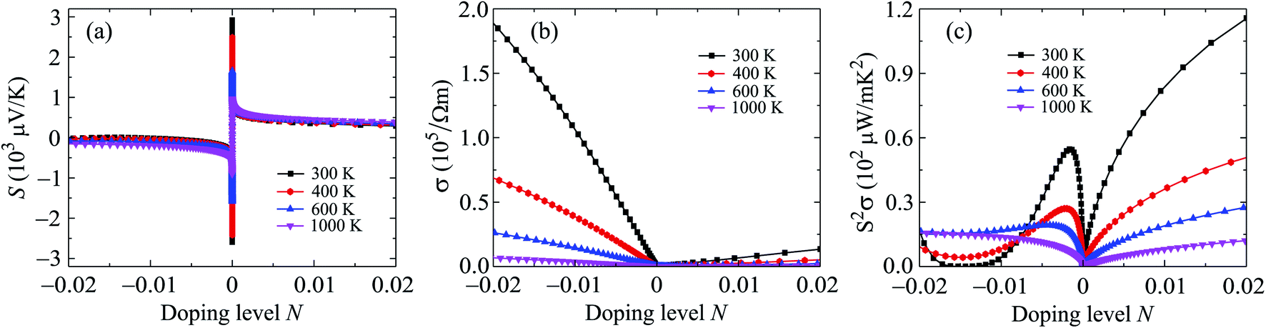 | ||
| Fig. 8 Seebeck coefficient S (a) electrical conductivity σ (b), and power factor S2σ (c) of Ga2SSe at different values of temperature. | ||
The key factor of thermal nanomaterials is the figure of merit ZT, which is evaluated by the expression36
 | (8) |
From eqn (8), we reveal that the magnitude of the total thermal conductivity κtot (κtot = κe + κl), especially the lattice part κl, is considered as a key factor in determining the value of the figure of merit ZT. In our calculations, the assumption of κl independent of the doping level N has been used, which has been properly proven in previous works.34,37 The thermal conductivity of Ga2SSe is depicted in Fig. 9. Our obtained results demonstrate that both κe and κl depend highly on temperature. As shown in Fig. 9(b), the Janus Ga2SSe exhibits a very low κl. The κl of Ga2SSe is only 0.028 W mK−1 at room temperature and it decreases with the increasing temperature. The N-dependent total thermal conductivity κtot at different values of temperature is shown in Fig. 9(b). We can see that the κtot decreases with the increasing temperature for both cases of doping type.
 | ||
| Fig. 9 (a) Doping level dependence of electronic conductivity κe, (b) temperature dependent lattice thermal conductivity κl, and (c) doping level dependence of total thermal conductivity κtot of Ga2SSe monolayer. | ||
Possessing very low κl, Ga2SSe is expected to have a high ZT, particularly in the high-temperature region. The calculated results for the dependence of ZT on the doping level N by the PBE + SOC method are presented in Fig. 10. At room temperature, the maximum ZT is up to 0.725 for the p-type doping. The value of ZT for the p-type doping is higher than that for the case of the p-type doping and we can increase ZT by temperature. In the doping level ranging from 0 to 0.02, the ZT of Ga2SSe can be increased to 0.817 at 1000 K. With very low thermal conductivity and high ZT, Ga2SSe has great potential for applications as thermoelectric materials.
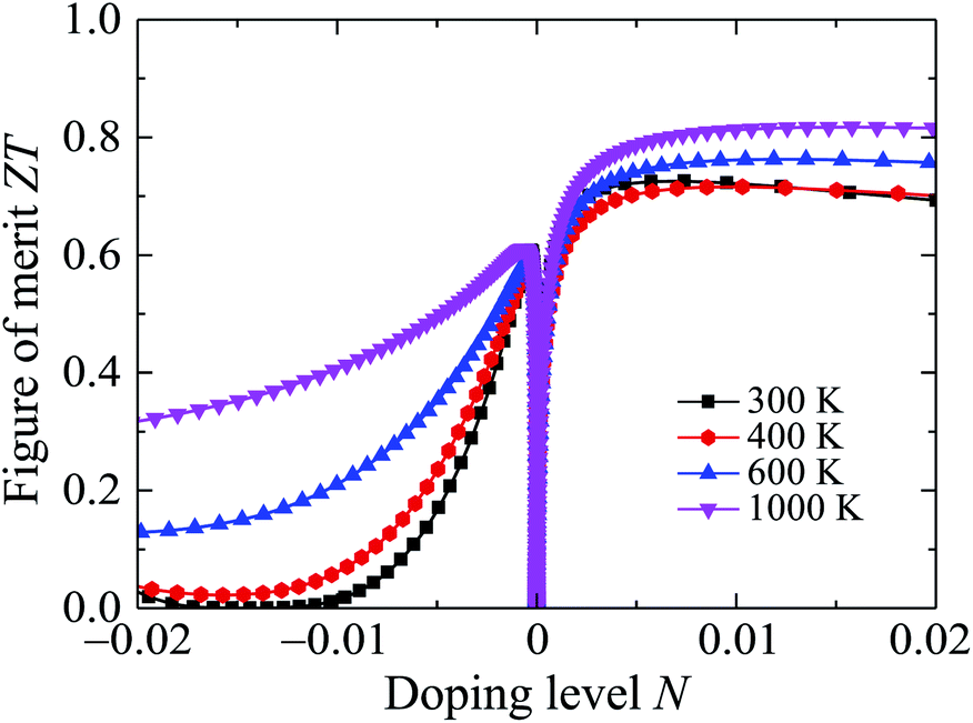 | ||
| Fig. 10 Doping level dependent figure of merit ZT of Ga2SSe at different values of temperature. | ||
4 Conclusion
In conclusion, we present a systematic investigation of the electronic, optical, and thermoelectric properties of Ga2SSe by using DFT calculations. The Janus Ga2SSe was confirmed to be dynamical and thermal stabilities via the phonon analysis and AIMD simulations. It is found that Ga2SSe exhibits an indirect characteristic semiconductor and its band gap can be driven by biaxial strain. The SOC not only reduces the band gap but also causes a small spin–orbit splitting of 90 meV in the valence band. The optical absorption spectrum of Ga2SSe is activated in the visible light and the first peak of the absorption spectrum locates in the near-ultraviolet region. With high absorption intensity, Ga2SSe is expected to have great potential for applications in optoelectronics. By solving the Boltzmann transport equations, the electronic transport coefficients have been investigated. Both PBE and PBE + SOC methods are used to calculate the electronic transport coefficients. Monolayer Ga2SSe exhibits a high ZT at room temperature and its ZT can be enhanced by temperature.Conflicts of interest
There are no conflicts to declare.Acknowledgements
This research is funded by Funds for Science and Technology Development of the University of Danang under project number B2019-DN03-43.References
- N. A. Poklonski, S. A. Vyrko, A. I. Siahlo, O. N. Poklonskaya, S. V. Ratkevich, N. N. Hieu and A. A. Kocherzhenko, Mater. Res. Express, 2019, 6, 042002 Search PubMed.
- A. I. Siahlo, N. A. Poklonski, A. V. Lebedev, I. V. Lebedeva, A. M. Popov, S. A. Vyrko, A. A. Knizhnik and Y. E. Lozovik, Phys. Rev. Mater., 2018, 2, 036001 Search PubMed.
- N. Poklonski, E. Kislyakov, N. N. Hieu, O. Bubel', S. Vyrko, A. Popov and Y. Lozovik, Chem. Phys. Lett., 2008, 464, 187 Search PubMed.
- A.-Y. Lu, H. Zhu, J. Xiao, C.-P. Chuu, Y. Han, M.-H. Chiu, C.-C. Cheng, C.-W. Yang, K.-H. Wei, Y. Yang, Y. Wang, D. Sokaras, D. Nordlund, P. Yang, D. A. Muller, M.-Y. Chou, X. Zhang and L.-J. Li, Nat. Nanotechnol., 2017, 12, 744 Search PubMed.
- J. Zhang, S. Jia, I. Kholmanov, L. Dong, D. Er, W. Chen, H. Guo, Z. Jin, V. B. Shenoy, L. Shi and J. Lou, ACS Nano, 2017, 11, 8192–8198 Search PubMed.
- Y. Sun, Z. Shuai and D. Wang, Nanoscale, 2018, 10, 21629 Search PubMed.
- D. D. Vo, T. V. Vu, N. V. Hieu, N. N. Hieu, H. V. Phuc, N. T. T. Binh, L. T. T. Phuong, M. Idrees, B. Amin and C. V. Nguyen, Phys. Chem. Chem. Phys., 2019, 21, 25849 Search PubMed.
- S.-D. Guo, X.-S. Guo, R.-Y. Han and Y. Deng, Phys. Chem. Chem. Phys., 2019, 21, 24620 Search PubMed.
- T. V. Vu, V. T. T. Vi, C. V. Nguyen, H. V. Phuc and N. N. Hieu, J. Phys. D: Appl. Phys., 2020, 53, 455302 Search PubMed.
- S.-D. Guo, X.-S. Guo and Y. Deng, J. Appl. Phys., 2019, 126, 154301 Search PubMed.
- A. Huang, W. Shi and Z. Wang, J. Phys. Chem. C, 2019, 123, 11388 Search PubMed.
- Q.-F. Yao, J. Cai, W.-Y. Tong, S.-J. Gong, J.-Q. Wang, X. Wan, C.-G. Duan and J. H. Chu, Phys. Rev. B, 2017, 95, 165401 Search PubMed.
- J. Yuan, Y. Shan and T. Li, J. Phys. D: Appl. Phys., 2020, 53, 125502 Search PubMed.
- T. V. Vu, H. D. Tong, D. P. Tran, N. T. T. Binh, C. V. Nguyen, H. V. Phuc, H. M. Do and N. N. Hieu, RSC Adv., 2019, 9, 41058 Search PubMed.
- X. Yang, D. Singh, Z. Xu, Z. Wang and R. Ahuja, J. Mater. Chem. C, 2019, 7, 12312–12320 Search PubMed.
- T. V. Vu, N. V. Hieu, H. V. Phuc, N. N. Hieu, H. Bui, M. Idrees, B. Amin and C. V. Nguyen, Appl. Surf. Sci., 2020, 507, 145036 Search PubMed.
- H. T. T. Nguyen, M. M. Obeid, A. Bafekry, M. Idrees, T. V. Vu, H. V. Phuc, N. N. Hieu, L. T. Hoa, B. Amin and C. V. Nguyen, Phys. Rev. B, 2020, 102, 075414 Search PubMed.
- X. Cheng, C. Zhang, L. Guan and J. Tao, Phys. Status Solidi B, 2019, 256, 1900070 Search PubMed.
- W. Wan, S. Zhao, Y. Ge and Y. Liu, J. Phys.: Condens. Matter, 2019, 31, 435501 Search PubMed.
- Y. Guo, S. Zhou, Y. Bai and J. Zhao, Appl. Phys. Lett., 2017, 110, 163102 Search PubMed.
- P. Giannozzi, S. Baroni, N. Bonini, M. Calandra, R. Car, C. Cavazzoni, D. Ceresoli, G. L. Chiarotti, M. Cococcioni, I. Dabo, A. D. Corso, S. de Gironcoli, S. Fabris, G. Fratesi, R. Gebauer, U. Gerstmann, C. Gougoussis, A. Kokalj, M. Lazzeri, L. Martin-Samos, N. Marzari, F. Mauri, R. Mazzarello, S. Paolini, A. Pasquarello, L. Paulatto, C. Sbraccia, S. Scandolo, G. Sclauzero, A. P. Seitsonen, A. Smogunov, P. Umari and R. M. Wentzcovitch, J. Phys.: Condens. Matter, 2009, 21, 395502 Search PubMed.
- J. P. Perdew, K. Burke and M. Ernzerhof, Phys. Rev. Lett., 1996, 77, 3865 Search PubMed.
- A. H. MacDonald, W. E. Picket and D. D. Koelling, J. Phys. C: Solid State Phys., 1980, 13, 2675 Search PubMed.
- S. Nosé, J. Chem. Phys., 1984, 81, 511 Search PubMed.
- G. K. Madsen and D. J. Singh, Comput. Phys. Commun., 2006, 175, 67 Search PubMed.
- A. Togo, L. Chaput and I. Tanaka, Phys. Rev. B: Condens. Matter Mater. Phys., 2015, 91, 094306 Search PubMed.
- A. Delin, P. Ravindran, O. Eriksson and J. Wills, Int. J. Quantum Chem., 1998, 69, 349 Search PubMed.
- S. Z. Karazhanov, P. Ravindran, A. Kjekshus, H. Fjellvag and B. G. Svensson, Phys. Rev. B: Condens. Matter Mater. Phys., 2007, 75, 155104 Search PubMed.
- P. Ravindran, A. Delin, B. Johansson, O. Eriksson and J. M. Wills, Phys. Rev. B: Condens. Matter Mater. Phys., 1999, 59, 1776–1785 Search PubMed.
- H. T. T. Nguyen, V. T. Vi, T. V. Vu, H. V. Phuc, C. V. Nguyen, H. D. Tong, L. T. Hoa and N. N. Hieu, Phys. E, 2020, 124, 114358 Search PubMed.
- D. R. Penn, Phys. Rev., 1962, 128, 2093 Search PubMed.
- L. D. Hicks and M. S. Dresselhaus, Phys. Rev. B: Condens. Matter Mater. Phys., 1993, 47, 16631(R) Search PubMed.
- S. Poncé, E. Margine, C. Verdi and F. Giustino, Comput. Phys. Commun., 2016, 209, 116–133 Search PubMed.
- Z. Jin, Q. Liao, H. Fang, Z. Liu, W. Liu, Z. Ding, T. Luo and N. Yang, Sci. Rep., 2015, 5, 18342 Search PubMed.
- G. Ding, J. He, Z. Cheng, X. Wang and S. Li, J. Mater. Chem. C, 2018, 6, 13269 Search PubMed.
- Y. Pei, X. Shi, A. LaLonde, H. Wang, L. Chen and G. J. Snyder, Nature, 2011, 473, 66 Search PubMed.
- W. Huang, H. Da and G. Liang, J. Appl. Phys., 2013, 113, 104304 Search PubMed.
| This journal is © The Royal Society of Chemistry 2020 |