DOI:
10.1039/D0RA07856E
(Paper)
RSC Adv., 2020,
10, 43187-43192
High quality N-polar GaN films grown with varied V/III ratios by metal–organic vapor phase epitaxy†
Received
14th September 2020
, Accepted 23rd November 2020
First published on 27th November 2020
Abstract
We studied the growths and characterizations of N-polar GaN films grown with constant and varied V/III ratios in high-temperature (HT) GaN growth on offcut c-plane sapphire substrates by metal–organic vapor phase epitaxy. It is found that growth with a constantly low V/III ratio resulted in a high crystallinity but a rough surface and a high oxygen concentration, whereas growth with a high V/III ratio led to a smooth surface but a high carbon concentration and a degraded crystallinity. The overall quality of the N-polar GaN epilayer cannot be effectively improved simply by tuning the V/III ratio. The growth with varied V/III ratios was conducted by lowering the V/III ratio in the initial HT-GaN growth and keeping the V/III ratio constantly high in the subsequent growth. Such a change of V/III ratio resulted in a 3D-to-2D like growth mode transition during the early stage of HT-GaN growth which helped reduce threading dislocations and suppress impurity incorporation. By optimizing the nucleation temperature and the thickness of the initial low-V/III-ratio layer, the minimum full-widths at half-maximum of (00![[2 with combining macron]](https://www.rsc.org/images/entities/char_0032_0304.gif) )/(10) rocking curves obtained were 288/350 arcsec and the oxygen concentration was reduced significantly from 1.6 × 1018 cm−3 to 3.7 × 1017 cm−3 while keeping a hillock-free smooth surface morphology. The overall quality of the N-polar GaN films was considerably improved. We believe that this simple, yet effective growth technique has great application prospects for high-performance N-polar GaN-based electron devices.
)/(10) rocking curves obtained were 288/350 arcsec and the oxygen concentration was reduced significantly from 1.6 × 1018 cm−3 to 3.7 × 1017 cm−3 while keeping a hillock-free smooth surface morphology. The overall quality of the N-polar GaN films was considerably improved. We believe that this simple, yet effective growth technique has great application prospects for high-performance N-polar GaN-based electron devices.
1. Introduction
The lack of inversion symmetry of the wurtzite GaN crystals along the c-axis produces two-polarities: Ga-polar and N-polar. Traditional devices are mostly fabricated on Ga-polar materials.1,2 However, the recent breakthroughs made in N-polar GaN-based high electron mobility transistors (HEMTs) have revealed the great potential of N-polar III-nitride materials in high-power and high-frequency applications. For example, N-polar HEMTs for high power switching have demonstrated a breakdown voltage as high as 2000 V,3 N-polar HEMTs for radio-frequency applications have demonstrated a record output power density of 8 W mm−1 at 94 GHz, surpassing any Ga-polar HEMT devices.4 Despite the exciting device performances, high quality N-polar GaN thin films are generally not so easily attainable as the Ga-polar ones. N-polar GaN films can be grown on nitridated c-plane sapphire, C-face SiC or N-face GaN substrates by metal–organic vapor phase epitaxy (MOVPE). Due to the low surface mobilities of adatoms, N-polar GaN surfaces are normally featured with a high density of hexagonal hillocks. By employing substrates with offcuts, the hexagonal hillocks can be completely mitigated but the surface may still present undulations/macro-steps. The surface steps affect the interface sharpness of the GaN/AlGaN hetero-structure and thus impact the concentration and mobility of the 2-dimensional electron gas (2DEG). Another difficulty in the N-polar GaN growth relates to the impurity incorporation. In the MOVPE growth, N-polar GaN films may be subject to high oxygen impurity incorporations. It is reported that the oxygen concentration can be over one order of magnitude higher in the N-polar GaN layer than that in the Ga-polar film that grown under the same condition.5 Since oxygen atoms behave as shallow donors in the GaN lattice matrices, the background electron concentration is high for N-polar materials, making it relatively difficult to realize high resistive N-polar GaN films. Further, N-polar GaN films are generally of poorer crystallinity compared to their Ga-polar counterparts. In a typical two-step growth of Ga-polar GaN by MOVPE, the threading dislocation density (TDD) can be reduced by a growth mode transition from 3-dimension (3D) to 2-dimension (3D). Assisted with a patterned substrate, the TDD can be reduced as low as 4.6 × 107 cm.6 However, a starting 3D surface morphology may seriously degrade the final surface morphology of N-polar films considering the low surface mobilities of adatoms on the N-polar surface. It has been reported that the growth of N-polar GaN films on nitridated planar sapphire substrates starts with a quasi-2D growth mode rather than a 3D mode.7 In such a scenario, the reduction of TDD in N-polar GaN films may be limited to growth parameter optimizations such as temperature, pressure, V/III ratio, and so on.
The V/III ratio in the MOVPE process of GaN growth is a critical parameter that impacts a series of material properties including surface morphology, impurity incorporation, and crystallinity. It is known that the adatom migration can be enhanced in the excess of Ga (a low V/III ratio). Therefore, a low V/III ratio in the order of several hundreds are commonly used in literature to suppress the formation of hexagonal hillocks on the N-polar GaN surface.2,8,9 However, a low V/III ratio tends to enhance the oxygen incorporation in the N-polar GaN. Although a high V/III ratio helps reduce the oxygen impurity concentration, it increases the possibility of a rough N-polar surface. In addition, the V/III ratio also plays a part in the growth mode transition. It is found that in the two-step growth of Ga-polar GaN films on a sapphire substrate by MOVPE, a low V/III ratio increases the 3D-to-2D transition duration and improves the crystallinity.10 In our previous report, we found that a low V/III ratio leads to a 3D-to-2D like growth mode transition but a relatively rough surface morphology in the N-polar GaN growth by MOVPE.11 Therefore, the overall quality of N-polar GaN films, i.e., surface roughness, impurity concentration, and TDD, cannot be effectively improved simply by increasing or decreasing the V/III ratio during the growth.
In this work, we studied the growths and characterizations of N-polar GaN films grown with varied V/III ratios in the high-temperature (HT) GaN growth by MOVPE. The surface morphologies, structural properties, impurity incorporations, and sheet carrier concentrations and electron mobilities were investigated in detail. The growths under the conditions of the varied V/III ratios were found to effectively improve the overall quality of the N-polar GaN films with a smooth surface, high crystallinity, and low impurity concentrations.
2. Experiment
N-polar GaN layers were grown on 2-inch c-plane sapphire substrates with 4°-offcut towards a-plane in an MOVPE reactor. The substrates were first processed at 1050 °C in H2 ambient to remove surface contaminations, then nitridated at 900 °C for 30 seconds in NH3 and N2 mixture. This surface nitridation is necessary for N-polarity control.12 After that, the growth of N-polar GaN was started with a ∼20 nm-thick low-temperature (650 °C or 900 °C) GaN (LT-GaN) nucleation followed by a high-temperature (1040 °C) GaN (HT-GaN) main layer. Hydrogen is used as the carrier gas. The reactor pressure was set to 100 mbar through the entire growth. Trimethyl-gallium (TMGa) and NH3 were used as the Ga and N precursors, respectively. Six different samples, denoted as A to F, were prepared. Samples A and B were grown with constantly low (128) and high (2237) V/III ratios (i.e. the molar ratio of NH3 to TMGa) in the HT-GaN growths, respectively. Samples C–E were grown with a low V/III ratio (128) in the initial HT-GaN growth and a high V/III ratio (2237) in the subsequent growth. The thickness of the low-V/III-ratio layer was increased from Sample C to E to study its effect on the film quality. The thickness of the high-V/III-ratio HT-GaN layer was varied according to the thickness of the low-V/III-ratio HT-GaN layer in order to maintain a similar total-thickness of the HT-GaN layers. The V/III ratio was controlled by fixing the TMGa supply while changing the NH3 flow rate. Sample F was prepared in the same procedure as Sample E except for a higher nucleation temperature (900 °C) of LT-GaN. Table 1 lists the key growth parameters of the N-polar GaN samples. Note that a 0 nm layer thickness means there is no such layer growth. The layer thicknesses are estimated based on the growth rate measured from the in situ optical reflectance curves.
Table 1 Key growth parameters of Samples A–F
| # |
LT-GaN temperature (°C) |
Low-V/III-ratio HT-GaN thickness (nm) |
High-V/III-ratio HT-GaN thickness (nm) |
| A |
650 |
1296 |
0 |
| B |
650 |
0 |
1350 |
| C |
650 |
11 |
1420 |
| D |
650 |
22 |
1410 |
| E |
650 |
86 |
1340 |
| F |
900 |
86 |
1330 |
3. Results and discussions
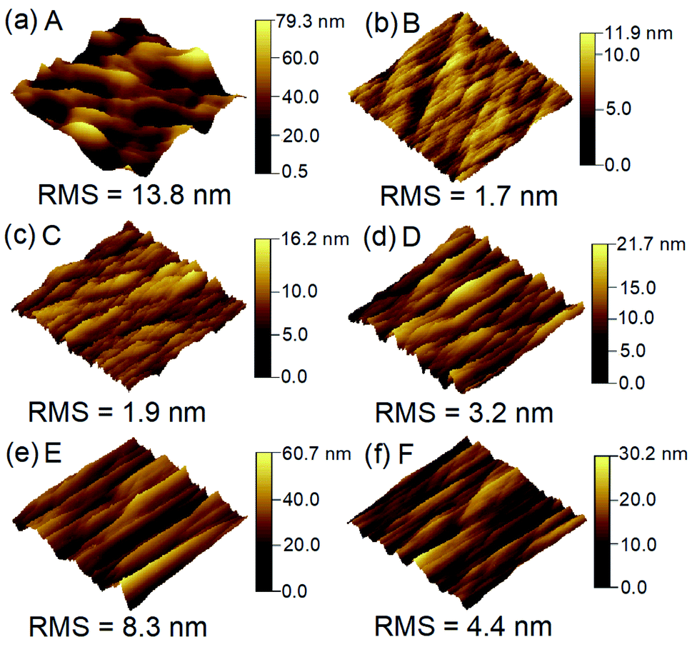
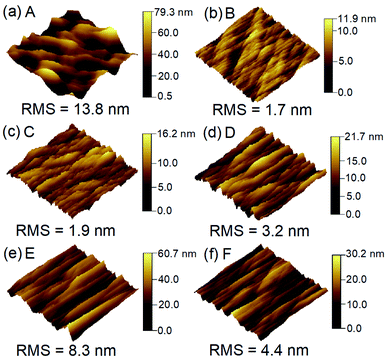
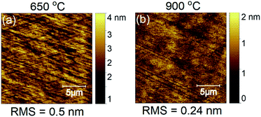
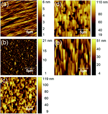
The surface morphologies of the N-polar samples were measured by an atomic force microscope (AFM) in tapping mode (Fig. 1). In general, all samples had prominent surface steps but no hexagonal hillocks. Sample A presented an undulated surface morphology with a high root-mean-square (RMS) roughness of 13.8 nm [Fig. 1(a)], whereas Sample B exhibited a much smoother surface with a reduced RMS roughness of 1.7 nm [Fig. 1(b)]. The rougher surface grown with the lower V/III ratio was previously explained by the non-uniform island formation in the initial HT-GaN growth and severe step-bunching effect.11 For Samples C–E, with increasing thickness of the low-V/III-ratio layer from 11 nm to 22 nm and to 86 nm, the RMS surface roughness was increased from 1.9 nm to 3.2 nm and to 8.3 nm. The surface roughness was reduced to 4.4 nm for Sample F, which should be attributed to a smoother buffer layer grown at a higher temperature (see Fig. 2). A similar high-temperature nucleation at 1050 °C has also been used to improve the surface morphology of N-polar GaN films by other groups.2,13 Note that the nitrogen polarities of all samples were verified by wet etching in potassium hydroxide hot solution (results shown in the supplement information).
 |
| | Fig. 1 Three-dimensional AFM height images (25 × 25 μm2) of the surface morphologies for Samples A–F. | |
 |
| | Fig. 2 AFM height images of the LT-GaN layer surfaces after high temperature annealing. The LT-GaN layers were grown at (a) 650 °C and (b) 900 °C. | |
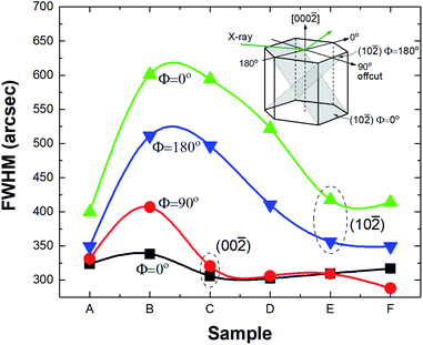
The structural properties of the N-polar samples were characterized by a high-resolution X-ray diffractometer (HRXRD). We previously reported that N-polar GaN layers grown on offcut sapphire substrates exhibited obvious structural anisotropies, in which the full width at half maximums (FWHMs) of the (00) plane rocking curves (RCs) varied with the azimuth angles.14 Such a structural anisotropy was physically attributed to the asymmetric nucleation behavior parallel and perpendicular to the offcut direction during the epitaxial growth.14,15 It should be mentioned that the structural anisotropy was mostly ignored or less stressed in earlier reports in the crystallinity evaluation of N-polar GaN films grown on offcut substrates. In this work, to accurately assess the overall structural properties of the N-polar GaN samples, we performed (00) and (10) RC scans at different azimuth angles and obtained the FWHMs of the RCs. The minimum and maximum FWHMs were then used to determine the crystallinities of all samples. The structural anisotropy was defined as the difference between the maximum and minimum FWHMs. Prior to the measurements, the GaN samples were carefully aligned so that the substrate offcut axis was perpendicular to the incident beam of the X-ray, which is schematically shown in the inset of Fig. 3. The azimuth angle Φ is defined as the angle between the GaN[110] axis with respect to the projection of the X-ray beam on the diffraction plane, i.e., Φ = 90° coincides the offcut direction (GaN[1![[1 with combining macron]](https://www.rsc.org/images/entities/char_0031_0304.gif) 00]). Fig. 3 shows the variations of the minimum and maximum FWHMs for (00) and (10) RCs sequentially from Sample A to Sample F. The minimum and maximum FWHMs of (00) RCs for Samples A–E were obtained at Φ = 0° and 90°, respectively, whereas the case is the opposite for Sample F. For (10) RCs, the minimum and maximum FHWMs were measured at Φ = 180° and 0°, respectively. One sees that Sample A has relatively lower FHWMs and smaller structural anisotropies than Sample B, indicating a lower TDD in the growth with a lower V/III ratio. From Sample B to Sample E, the minimum and maximum FWHMs of (00) and (10) RCs and the structural anisotropies in (00) plane declined with increasing thickness of the low-V/III-ratio layer, but their structural anisotropies in (10) plane are similar. Sample F had a similar crystallinity to Sample E but an enlarged structural anisotropy in (00) plane, implying a minor effect of the nucleation temperature on the crystal quality of the HT-GaN layer. The lowest FWHMs of (00) RCs and (10) RCs obtained are 288 arcsec and 350 arcsec (Sample F), respectively.
00]). Fig. 3 shows the variations of the minimum and maximum FWHMs for (00) and (10) RCs sequentially from Sample A to Sample F. The minimum and maximum FWHMs of (00) RCs for Samples A–E were obtained at Φ = 0° and 90°, respectively, whereas the case is the opposite for Sample F. For (10) RCs, the minimum and maximum FHWMs were measured at Φ = 180° and 0°, respectively. One sees that Sample A has relatively lower FHWMs and smaller structural anisotropies than Sample B, indicating a lower TDD in the growth with a lower V/III ratio. From Sample B to Sample E, the minimum and maximum FWHMs of (00) and (10) RCs and the structural anisotropies in (00) plane declined with increasing thickness of the low-V/III-ratio layer, but their structural anisotropies in (10) plane are similar. Sample F had a similar crystallinity to Sample E but an enlarged structural anisotropy in (00) plane, implying a minor effect of the nucleation temperature on the crystal quality of the HT-GaN layer. The lowest FWHMs of (00) RCs and (10) RCs obtained are 288 arcsec and 350 arcsec (Sample F), respectively.
 |
| | Fig. 3 The minimum and maximum FWHMs of GaN(00) and GaN(10) RCs measured at different Φ values. The inset illustrates the XRD optical alignment with respect to the GaN crystal geometry. | |
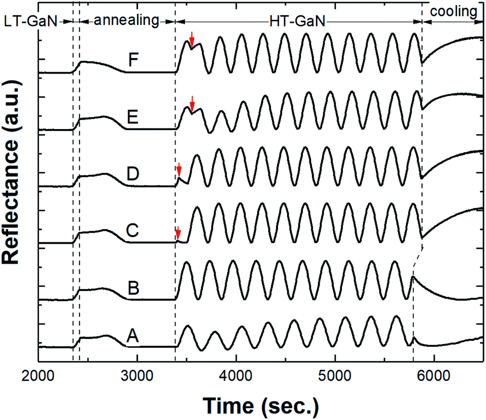
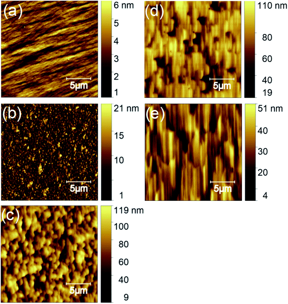
In the hetero-epitaxy process, the thin film crystal quality is usually correlated with its growth mode, which also affects the surface morphology. For the N-polar samples grown with constant V/III ratios, the low V/III ratio led to rough surface but high crystal quality (Sample A), whereas the high V/III ratio improved the surface morphology but compromised the structural properties (Sample B). Such discrepancies originate from the different growth modes under different V/III ratios, which can be verified from the in situ optical reflectance curves of Samples A and B (Fig. 4). In our last work, we have observed larger size but lower density nuclei in the initial HT-GaN growth stage and a higher step-bunching effect under a condition of lower V/III ratio, which was believed to be the cause of the rougher surface.11 In the proceeding growth, the large islands tended to coalesce and transit to a 2D-like growth mode.11 In such a process, threading dislocations (TDs) can partially bend and annihilate and eventually result in an improved crystallinity, similar to that in the typical two-step growth of Ga-polar GaN.10,16,17 Therefore, the lacking of the 3D-to-2D growth mode transition in the growth with a high V/III ratio can cause an inferior crystal quality. In the growths with varied V/III ratios (Samples C–F), the initial low-V/III-ratio layer should provide a similar 3D-like surface, which was later transformed to a 2D morphology as the lateral growth was enhanced in the proceeding growth at a high V/III ratio. Fig. 5(a–e) show the surface morphologies of the initial HT-GaN layers with increasing thicknesses grown in the same procedure of Sample E. One can see a clear trend of 3D-island coalescence as the growth proceeded. An increase in the thickness of the low-V/III-ratio layer further roughened the starting surface morphology [Fig. 5(a–c)] and enhanced the 3D growth mode, resulting a prolonged recovery time of the optical reflectance from Sample C to E (Fig. 4). Consequently, the TDD was further reduced and the resulting surface roughness was increased from Sample C to Sample E. Similar findings have been reported in the Ga-polar GaN growths in which a prolonged 3D islands coalescence leads to a higher crystallinity but rougher macroscopic surface morphology.17 However, the HT-GaN surface roughness can be reduced by simply employing a higher temperature of the LT-GaN layer without degrading the crystallinity (Sample F). We believe the resulting surface roughness can be further reduced if the LT-GaN growth conditions such as V/III ratio, pressure, and thickness are carefully optimized. In addition, the growth mode in the initial stage of HT-GaN growth may also affect the structural anisotropy. A 2D growth mode tends to enlarge the structural anisotropy, which we speculate is due to the increased nucleation discrepancy between the directions parallel and perpendicular to the offcut axis as a consequence of the enhanced lateral growth at high V/III ratio. More research is being conducted on this topic.
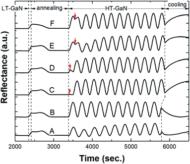 |
| | Fig. 4 In situ optical reflectance curves for Samples A–F. The arrows indicate the end time of the low-V/III-ratio HT-GaN layer growths of Samples C–F. | |
 |
| | Fig. 5 AFM images of (a) 11 nm, (b) 22 nm, (c) 86 nm low-V/III-ratio HT-GaN layers, and (d) 120 nm and (e) 240 nm high-V/III-ratio HT-GaN layers grown in the same procedure of Sample E. | |
Fig. 6(a) plots the room-temperature photoluminescence (PL) spectra of the N-polar GaN samples. In general, the spectra were dominated by the band edge emissions (BEs) of GaN peaked at 362 nm without obvious wavelength shift from sample to sample. A slight linewidth narrowing of BEs can be seen from Sample A to F, implying a decreasing trend of the free carrier density.18 Beside the dominant BEs, one sees broad side-luminescence (SL) bands covering the blue and yellow luminescence from 430–640 nm for all samples. The main peak of SL resided at ∼550 nm. Fig. 6(b) plots the variation in the SL-to-BE integrated intensity ratio (ISL/IBE) from Sample A to Sample F. It is clearly seen that ISL/IBE drastically declined from 1.95 to 0.075 from Sample A to Sample F. Physically, the relative intensity of SL is closely associated with the impurity incorporations in GaN. Oxygen and carbon are two major impurities in the GaN growth by MOVPE.5 Oxygen impurities, i.e. ON, usually behave as shallow donors and carbon impurities, i.e. CN, act as deep acceptors.19,20 For Sample A, there may exist abundant another type of shallow donors, i.e. nitrogen vacancies, VN, in the GaN lattice as insufficient NH3 was supplied during the growth. The broad yellow luminescence in the SL band should be attributed to the electron transitions from shallow-donor energy levels to deep-acceptor ones. In this light, the drastic decline of ISL/IBE from Sample A to Sample F may suggest a significant reduction of impurities.
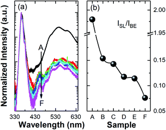 |
| | Fig. 6 Normalized PL spectra of Samples A–F (a), and the ISL/IBE ratios in the PL spectra of Samples A–F (b). | |
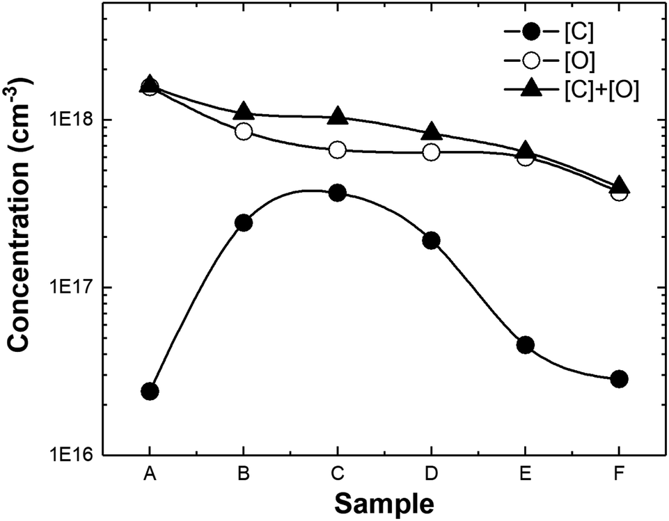
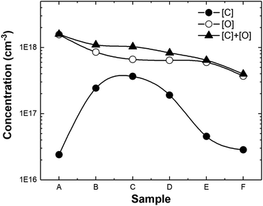
To quantify the impurity incorporations of the N-polar samples, secondary ion mass spectroscopy (SIMS) was used to extract the carbon and oxygen concentrations in Samples A–F. Fig. 7 plots the variations of the carbon and oxygen impurities concentrations from Sample A to Sample F. One sees that the carbon concentrations ([C]) first increased from Sample A to Sample C and then decreased from Sample C to Sample F, but the oxygen concentrations ([O]) and the overall oxygen and carbon concentration, i.e., [O] + [C], continuously declined from Sample A to Sample F. Sample A had the highest oxygen concentration (∼1.6 × 1018 cm−3) but the lowest carbon concentration (∼2.4 × 1016 cm−3). Sample F had the lowest oxygen concentration (∼3.7 × 1017 cm−3) and a slightly higher carbon concentration (∼2.8 × 1016 cm−3) than Sample A. It has been reported that the impurity incorporations in the GaN growth can be affected by V/III ratio, TDD and polarity. In Ga-polar GaN growth, a higher V/III ratio normally leads to a lower oxygen and carbon concentrations.21–23 In N-polar GaN growth, Fichtenbaum et al. found that the V/III ratio has a similar effect on the oxygen impurity concentration but little effect on the carbon incorporations.5 Early studies revealed that there is also a strong dependence of impurity concentrations on TDD.24 If TDD is high, more impurities tend to be incorporated due to the lower formation energies of impurities near the TD cores.24–26 Therefore, we believe that for Samples A and B, the difference in oxygen concentrations is mainly caused by the V/III ratio, whereas the variation in carbon concentrations is mainly due to the crystallinity difference. In addition, the continuously decreasing overall oxygen and carbon concentration from Sample C to Sample F should be also attributed to the reduction of TDD. It is noted that the variation in oxygen concentrations from Sample A to Sample F correlates well with the change of ISL/IBE, suggesting that oxygen impurities are the major cause of SL.
 |
| | Fig. 7 The concentrations of carbon and oxygen impurities of Samples A–F. | |
Finally, Hall measurements were carried out to test the sheet carrier concentrations, electron mobilities, and sheet resistances of the N-polar samples, and the results are listed in Table 2. All N-polar films were still very conductive, indicating an unintentionally N-doped property. From Sample A to Sample F, there are a significant reduction in sheet carrier concentrations from 1.48 × 1014 cm−2 to 3.69 × 1013 cm−2 and a ∼2-fold increase in both mobility and sheet resistance. Such considerable improvements should be also the results of the reduced impurity incorporations and the improved crystallinity of the samples grown with varied V/III ratios.
Table 2 Hall measurement results of Samples A–F
| Sample # |
Sheet carrier concentration (cm−2) |
Mobility (cm2 V−1 s−1) |
Sheet resistance (Ω □−1) |
| A |
−1.48 × 10¹⁴ |
256 |
174 |
| B |
−6.32 × 10¹³ |
337 |
304 |
| C |
−5.23 × 10¹³ |
374 |
318 |
| D |
−5.11 × 10¹³ |
395 |
320 |
| E |
−3.97 × 10¹³ |
443 |
382 |
| F |
−3.69 × 10¹³ |
445 |
380 |
4. Conclusion
In summary, we have studied the surface morphologies, structural properties, PL, impurity incorporations, sheet carrier concentrations, and electron mobilities of N-polar GaN thin films grown with varied V/III ratios. It is found that the overall quality of the N-polar GaN films, including surface roughness, crystallinity, and impurity concentration, cannot be improved at the same time by simply tuning the V/III ratio. By lowering the V/III ratio in the initial growth of the HT-GaN and keeping a high V/III ratio in the subsequent growth, a 3D-to-2D like growth mode transition can be achieved. Through such a growth scheme with varied V/III ratios and optimized nucleation temperature, high quality N-polar GaN films with a smooth surface, high crystallinity, low impurity and sheet carrier concentrations, and high electron mobility have been successfully achieved.
Conflicts of interest
There are no conflicts of interest to declare.
Acknowledgements
The work was supported by the China Postdoctoral Science Foundation (2019M662823), the Science and Technology Program of Guangzhou (201904010140), the Guangdong Academy of Sciences (2019GDASYL-0102008, 2018GDASCX-0801, 2017GDASCX-01, 2019GDASYL-0503007, 2020GDASYL-20200302012, and 2018GDASCX-0112), the Science and Technology Program of Guangdong (2017B010112002) and the National Key Research and Development Program of China (2017YFB0404102 and 2018YFB0406601).
References
- J. Zúñiga-Pérez, V. Consonni, L. Lymperakis, X. Kong, A. Trampert, S. Fernández-Garrido, O. Brandt, H. Renevier, S. Keller, K. Hestroffer, M. R. Wagner, J. S. Reparaz, F. Akyol, S. Rajan, S. Rennesson, T. Palacios and G. Feuillet, Appl. Phys. Rev., 2016, 3, 041303 Search PubMed.
- S. Keller, H. Li, M. Laurent, Y. Hu, N. Pfaff, J. Lu, D. F. Brown, N. A. Fichtenbaum, J. S. Speck, S. P. DenBaars and U. K. Mishra, Semicond. Sci. Technol., 2014, 29, 113001 CrossRef.
- O. S. Koksaldi, J. Haller, H. Li, B. Romanczyk, M. Guidry, S. Wienecke, S. Keller and U. K. Mishra, IEEE Electron Device Lett., 2018, 39, 1014–1017 CAS.
- B. Romanczyk, S. Wienecke, M. Guidry, H. Li, E. Ahmadi, X. Zheng, S. Keller and U. K. Mishra, IEEE Trans. Electron Devices, 2018, 65, 45–50 CAS.
- N. A. Fichtenbaum, T. E. Mates, S. Keller, S. P. DenBaars and U. K. Mishra, J. Cryst. Growth, 2008, 310, 1124–1131 CrossRef CAS.
- C. He, W. Zhao, K. Zhang, L. He, H. Wu, N. Liu, S. Zhang, X. Liu and Z. Chen, ACS Appl. Mater. Interfaces, 2017, 9, 43386–43392 CrossRef CAS.
- Q. Sun, Y. S. Cho, I.-H. Lee, J. Han, B. H. Kong and H. K. Cho, Appl. Phys. Lett., 2008, 93, 131912 CrossRef.
- J. Song, S.-P. Chang, C. Zhang, T.-C. Hsu and J. Han, ACS Appl. Mater. Interfaces, 2015, 7, 273–278 CrossRef CAS.
- J. Song, G. Yuan, K. Xiong, B. Leung and J. Han, Cryst. Growth Des., 2014, 14, 2510–2515 CrossRef CAS.
- D. G. Zhao, D. S. Jiang, J. J. Zhu, Z. S. Liu, S. M. Zhang, H. Yang and J. W. Liang, J. Cryst. Growth, 2007, 303, 414–418 CrossRef CAS.
- C. Li, K. Zhang, Q. Zeng, Q. Wang, Z. Li, W. Zhao and Z. Chen, J. Cryst. Growth, 2020, 536, 125599 CrossRef CAS.
- M. Sumiya, MRS Internet J. Nitride Semicond. Res., 2004, 9, 1–32 CrossRef.
- N. A. Fichtenbaum, PhD thesis, University of California, Santa Barbara, 2008, https://search.proquest.com/docview/304665690/abstract?accountid=13876.
- C. Li, H. Wang, H. Liu and S. J. Chua, J. Vac. Sci. Technol., A, 2016, 34, 051501 CrossRef.
- J. Kato, S. Tanaka, S. Yamada and I. Suemune, Appl. Phys. Lett., 2003, 83, 1569–1571 CrossRef CAS.
- M. A. Moram, C. S. Ghedia, D. V. S. Rao, J. S. Barnard, Y. Zhang, M. J. Kappers and C. J. Humphreys, J. Appl. Phys., 2009, 106, 073513 CrossRef.
- S. Kim, J. Oh, J. Kang, D. Kim, J. Won, J. W. Kim and H.-K. Cho, J. Cryst. Growth, 2004, 262, 7–13 CrossRef CAS.
- C. Li, H. Liu and S. J. Chua, J. Appl. Phys., 2015, 117, 125305 CrossRef.
- V. Kirilyuk, M. Zielinski, P. c. m. Christianen, A. r. a. Zauner, J. l. Weyhera, P. r. Hageman and P. k. Larsen, in Symposium G – GaN and Related Alloys-2000, 2000, vol. 639 Search PubMed.
- M. A. Reshchikov and H. Morkoç, J. Appl. Phys., 2005, 97, 061301 CrossRef.
- D. D. Koleske, A. E. Wickenden, R. L. Henry and M. E. Twigg, J. Cryst. Growth, 2002, 242, 55–69 CrossRef CAS.
- A. Ishibashi, H. Takeshi, M. Mannoh, Y. Yabuuchi and Y. Ban, J. Electron. Mater., 1996, 25, 799–803 CrossRef CAS.
- S. Mita, R. Collazo, A. Rice, R. F. Dalmau and Z. Sitar, J. Appl. Phys., 2008, 104, 013521 CrossRef.
- S. Hashimoto, Y. Yoshizumi, T. Tanabe and M. Kiyama, J. Cryst. Growth, 2007, 298, 871–874 CrossRef CAS.
- J. Elsner, R. Jones, M. I. Heggie, P. K. Sitch, M. Haugk, Th. Frauenheim, S. Öberg and P. R. Briddon, Phys. Rev. B: Condens. Matter Mater. Phys., 1998, 58, 12571–12574 CrossRef CAS.
- A. Armstrong, T. A. Henry, D. D. Koleske, M. H. Crawford, K. R. Westlake and S. R. Lee, Appl. Phys. Lett., 2012, 101, 162102 CrossRef.
Footnote |
| † Electronic supplementary information (ESI) available. See DOI: 10.1039/d0ra07856e |
|
| This journal is © The Royal Society of Chemistry 2020 |
Click here to see how this site uses Cookies. View our privacy policy here. 
 Open Access Article
 This Open Access Article is licensed under a Creative Commons Attribution-Non Commercial 3.0 Unported Licence
 *,
Kang Zhang,
Qiaoyu Zeng,
Xuebing Yin,
Xiaoming Ge,
Junjun Wang,
Qiao Wang,
Chenguang He,
Wei Zhao and
Zhitao Chen
*,
Kang Zhang,
Qiaoyu Zeng,
Xuebing Yin,
Xiaoming Ge,
Junjun Wang,
Qiao Wang,
Chenguang He,
Wei Zhao and
Zhitao Chen