
 Open Access Article
 This Open Access Article is licensed under a
 Creative Commons Attribution 3.0 Unported Licence
Tuning the physical properties of ultrathin transition-metal dichalcogenides via strain engineering
Yalan Yan
 a,
Shuang Ding
a,
Xiaonan Wu
*c,
Jian Zhu
b,
Dengman Feng
b,
Xiaodong Yang
*a and
Fangfei Li
*b
a,
Shuang Ding
a,
Xiaonan Wu
*c,
Jian Zhu
b,
Dengman Feng
b,
Xiaodong Yang
*a and
Fangfei Li
*b
aInstitute for Interdisciplinary Biomass Functional Materials Studies, Jilin Engineering Normal University, No. 3050 Kaixuan Road, Changchun 130052, People's Republic of China. E-mail: y86908051@126.com
bState Key Laboratory of Superhard Materials, College of Physics, Jilin University, No. 2699 Qianjin Street, Changchun 130012, People's Republic of China. E-mail: lifangfei@jlu.edu.cn
cDepartment of Chemical Engineering, Chengde Petroleum College, Chengde 067000, People's Republic of China. E-mail: cdpcwxn2007@163.com
First published on 27th October 2020
Abstract
Transition-metal dichalcogenides (TMDs) have become one of the recent frontiers and focuses in two-dimensional (2D) materials fields thanks to their superior electronic, optical, and photoelectric properties. Triggered by the growing demand for developing nano-electronic devices, strain engineering of ultrathin TMDs has become a hot topic in the scientific community. In recent years, both theoretical and experimental research on the strain engineering of ultrathin TMDs have suggested new opportunities to achieve high-performance ultrathin TMDs based devices. However, recent reviews mainly focus on the experimental progress and the related theoretical research has long been ignored. In this review, we first outline the currently employed approaches for introducing strain in ultrathin TMDs, both their characteristics and advantages are explained in detail. Subsequently, the recent research progress in the modification of lattice and electronic structure, and physical properties of ultrathin TMDs under strain are systematically reviewed from both experimental and theoretical perspectives. Despite much work being done in this filed, reducing the distance of experimental progress from the theoretical prediction remains a great challenge in realizing wide applications of ultrathin TMDs in nano-electronic devices.
 Yalan Yan | Yalan Yan is an associate professor at Jilin Engineering Normal University. Her current research is on the modification of optical and electrical transport properties of ultrathin TMDs under strain. She was supported by the Jilin Engineering Normal University PhD startup foundation. |
 Shuang Ding | Shuang Ding is an associate professor at Jilin Engineering Normal University. Her current research is on the fabrication of photoelectric devices based on two-dimensional materials. |
 Xiaonan Wu | Xiaonan Wu is a professor at Chengde Petroleum College. His current research is on the modification of the physical properties of two-dimensional materials under high pressure. |
 Jian Zhu | Jian Zhu is a doctor at the College of Physics, Jilin University. His current research is on the modification of the physical properties of ultrathin TMDs under high pressure. |
 Dengman Feng | Dengman Feng is a master at the College of Physics, Jilin University. Her current research is on the preparation and the modification of optical properties of two-dimensional materials under strain. |
 Xiaodong Yang | Xiaodong Yang is a professor at Jilin Engineering Normal University. His current research is on the modification of magnetic properties of low dimensional nano-materials under strain. |
 Fangfei Li | Fangfei Li is a professor at the College of Physics, Jilin University. Her current research is on the modification of optical properties of two-dimensional materials, nanocarbon materials, and novel low-dimensional semiconductor optoelectronic materials. She was supported by the National Key Research and Development Program. |
Introduction
Since the successful exfoliation of graphene from graphite in 2004,1 2D materials have attracted great attention in the scientific community thanks to their novel physical properties.2–6 Among all the 2D materials, TMDs with the formula MX2, where M is a transition mental element and X is a chalcogen, assume a central place in the research of layered materials, since these materials possess great potential in the fields of electronics, optics and optoelectronics,7,8 and they are chemically versatile and naturally abundant. TMDs usually crystalize in three types, namely 2H-MX2, 1T-MX2, and 3R-MX2, depending on the stacking configuration of X–M–X.9 In each X–M–X layer, the M–X bond is strongly covalent, while adjacent layers are weakly coupled by van der Waals (vdW) interactions, resulting in a distinctive easy slippage and easy cleavage of planes in TMDs.At present, the synthesis of ultrathin TMDs has been widely investigated and many excellent review papers are available.10–12 However, these materials may not be directly useful for applications requiring properties other than their natal ones. Thus, it is the right time to think about not only synthesizing materials but also modifying their physical properties. Considering the fact that, ultrathin TMDs are intrinsically capable of sustaining much larger mechanical strain when compared to their bulk counterparts,13–15 meanwhile, for ultrathin TMDs based nanoscale devices, the TMDs films are usually under strain, thus, strain engineering should be a perfect approach to bring in novel and superior physical properties in ultrathin TMDs by tuning their lattice and electronic structure. In detail, strain can effectively change atomic bond-configuration (bond length, bond angle and bond strength) and the interaction between electronic orbitals, resulting in the emergence of novel phenomena and properties in ultrathin TMDs, such as thermal, electronic, optical, and magnetic properties. In this way, the capability to change the intrinsic properties of ultrathin TMDs through strain engineering has created tremendous opportunities for their applications in a variety of fields, including sensing, electronic and photoelectric devices, and so on.
At present, the study subjects of recent reviews on the strain engineering of ultrathin films are usually extended to 2D materials, including graphene, black phosphorus, BN, and TMDs, etc. For instance, Liu et al. summarized the current methods of introducing strain into 2D materials by classifying the deformation modes, and reviewed the crucial role of 2D material-substrate interfaces in governing these deformations.16 Sun et al. discussed the fundamentals of strain engineering in 2D materials from macro and atomic perspective and illuminated the effects of strain on the physical and chemical properties in 2D materials.17 Roldán et al. reviewed the recent progress in controlling the optical and electronics properties of 2D materials by strain engineering.18 Considering the fact that, the various 2D materials have their obviously different responses to strain, it should be mentioned that, narrowing the scope of study subjects to a smaller group will lead to a more systematic summary of strain engineering in ultrathin film, thus, a more systematic review on the strain engineering of ultrathin TMDs should be of great significance.
In this review, we focus on the recent development on the regulation of physical properties of ultrathin TMDs via strain engineering, we first discuss the characteristics of currently employed approaches for introducing strain by external force, subsequently, the recent advances on the strain engineering of ultrathin TMDs are reviewed by categorizing the physical properties, moreover, some of the bottle-neck problems in current researches are also pointed out.
Strain engineering for ultrathin TMDs
Approaches for introducing strain
Up to now, various experimental methods and strategies for generating strain have been implemented to explore novel physical properties in ultrathin TMDs, including externally exerted strain and internally evoked strain. External strain mainly involves external force, or stimulation, such as bending, stretching of flexible substrates and substrate thermal expansion. While internal strain mainly originates from multiple components and surface/interface interactions, which are closely related to defects, or lattice mismatches. Despite the diversity of experimental strategies for generating strain, an effectively controllable strain should be of great significant to obtain a targeted physical property, which is difficult to obtain by taking advantage of internal evoked strain owing to the unmanageable defects and lattice mismatches. Thus, in this review, we mainly focus on the research progress in the structures and properties of TMDs films under external strain.In this section, we summarize the feasible and currently employed approaches for introducing external strain in ultrathin TMDs: bending a flexible substrate, polymer-based encapsulation, formation of wrinkles, patterned substrate, atomic force microscope (AFM)-based apparatus, substrate thermal expansion, piezoelectric stretching, and diamond anvil cells (DAC). The schematic diagrams of experimental approaches for generating external strain are presented in Fig. 1 as below.
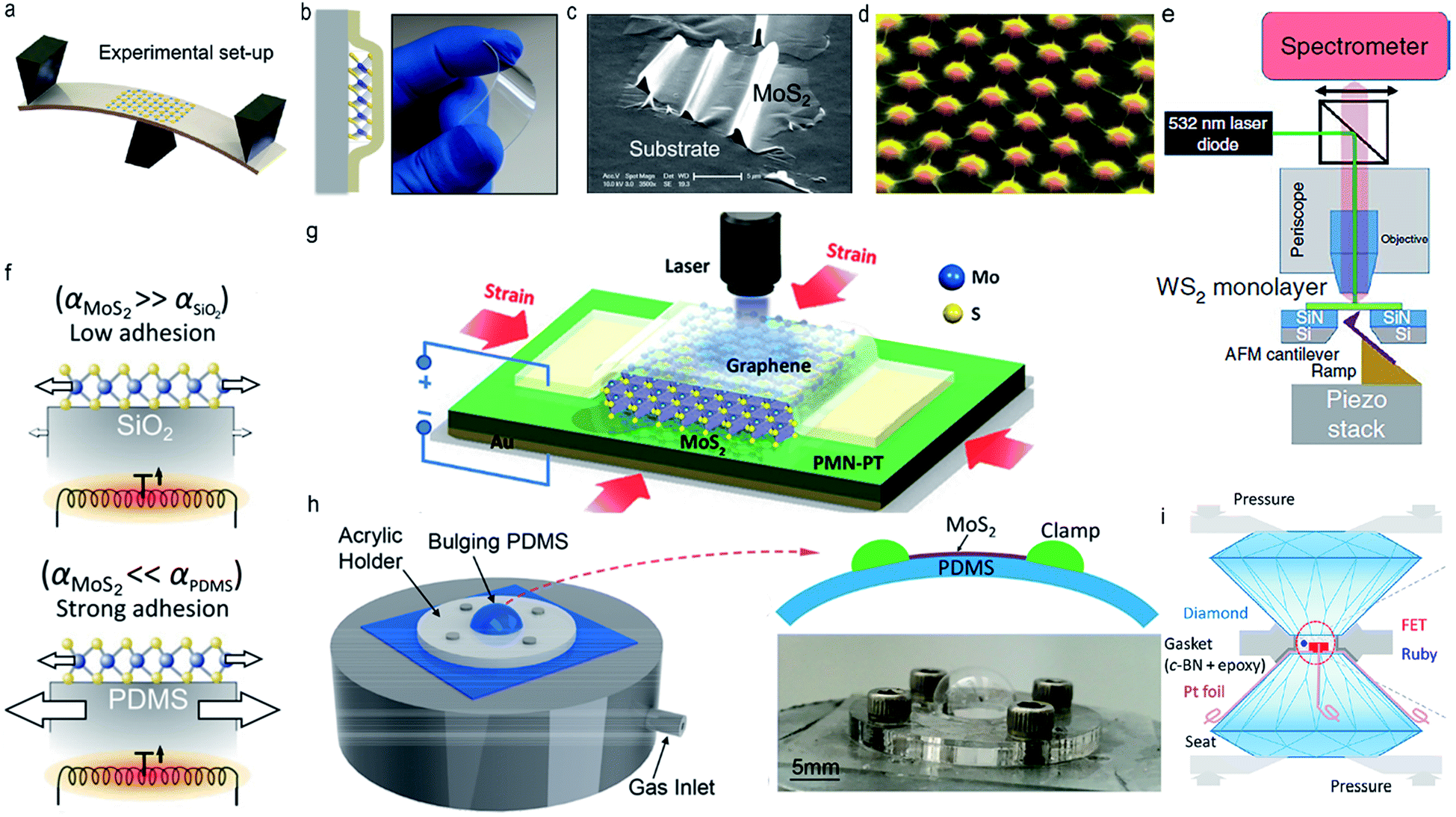 | ||
| Fig. 1 The schematic diagram of approaches for introducing external strain. (a) The three-point bending apparatus. Reproduced with permission.19 Copyright 2013, American Physical Society. (b) Large strain magnitude can be introduced in polymer encapsulated monolayer WSe2 by bending apparatus. Reproduced with permission.20 Copyright 2018, American Chemical Society. (c) Wrinkled monolayer MoS2 fabricated by prestretching an elastomeric substrate. Reproduced with permission.21 Copyright 2013, American Chemical Society. (d) Strained monolayer MoS2 indented by SiO2 nanocones, where the strain on the tips of nanocones exhibit highest while the strain between nanocones is lowest. Reproduced with permission.22 Copyright 2015, Nature. (e) Schematic of an atomic force microscope (AFM)-based apparatus. Reproduced with permission.23 Copyright 2020, Nature. (f) Schematic of the thermal-expansion induced strain in monolayer MoS2. Reproduced with permission.27 Copyright 2015, Institute of Physics. (g) Schematic diagram of optical measurements on strained trilayer MoS2 which is sandwiched between a piezoelectric substrate and a graphene electrode. Reproduced with permission.28 Copyright 2013, American Chemical Society. (h) Experimental setup for blown-bubble bulge measurement, high strain can be achieved in suspended MoS2 films by slowly diffusing N2 gas through the PDMS substrate to pressurize the cavity. Reproduced with permission.29 Copyright 2017, American Chemical Society. (i) Schematic of the electrical conductance measurements of few-layer MoS2 in a diamond anvil cells. Reproduced with permission.30 Copyright 2017, American Chemical Society. | ||
According to the previous reports, by bending/streching a flexible substrate, a uniaxial tensile strain of up to 4% can be acquired in ultrathin TMDs,19,31 as long as the TMDs membranes can be easily transferred and attached to the hosting substrate (Fig. 1a).
Despite the universal application of this technique above, it also presents some serious shortcomings, such as the difficulties in verifying the applied strain and obtaining large strain magnitude. In view of the above-mentioned bottlenecks, a novel polymer-based encapsulation method was developed to obtain large range accurate, uniform, highly repeatable, and independently measurable strain in ultrathin TMDs. In detail, firstly, ultrathin MoS2 was lifted from the SiO2/Si substrate by using cellulose acetate butyrate, then it was encapsulated between two polycarbonate substrates which are tightly bonded together, in this way, strain can be introduced in ultrathin MoS2 by bending the polymer substrate20 (Fig. 1b).
In addition, strain can also be brought in by fabricating wrinkles in supported ultrathin TMDs. Firstly, the elastomeric substrate was prestretched, on which ultrathin MoS2 was deposited, subsequently, the prestretching strain in elastomeric substrate is suddenly released and wrinkles generate in loaded ultrathin TMDs due to the buckling-induced delamination. In this way, local strain is attained in TMDs film thanks to the large deformation in wrinkled zone21 (Fig. 1c). It is notable that the amplitude and periodicity of wrinkles in ultrathin TMDs depend largely on the prestreching strain in elastomeric substrate and the releasing rates of prestrain.
Owing to the flexible characters of ultrathin TMDs and their van der Waals interaction to the substrate, local deformation of TMDs films can be directly obtained by transferring TMDs films onto a patterned substrate. This strategy has led to the rapid development of pattern design of substrate, along with the studies on the strain-induced interface chemistry and physics in ultrathin TMDs. For example, Mangu et al. established a locally varying strain fields in 6 layer MoS2 through conformal contact of ultrathin MoS2 with a textured Si substrate, realizing the facilely modification of the electronic band structure of ultrathin MoS2.32 Zheng et al. designed a strained MoS2 film using a patterned nanocone substrate and discussed their application in the hydrogen evolution reaction and bandgap engineering22,33,34 (Fig. 1d).
In addition, an AFM-based setup is also an effective approach to introduce non-uniform mechanical strain in ultrathin TMDs by indenting the film with an AFM tip.23–26 As shown in Fig. 1e, the WS2 monolayer suspended on top of a hole in the substrate membrane is indented from the bottom by an AFM cantilever and being optically interrogated from the top, in this way, the dynamics of the excited carriers in strained monolayer WS2 can be revealed by optical spectroscopy.23
It is worth mentioning that approaches in Fig. 1a–c can only introduce a uniaxial strain, however, the effect of biaxial strain in modifying the physical properties of ultrathin TMDs is obviously stronger than that of uniaxial strain (a more detailed discussion is presented in Section 2.2), thus, experimental realization of biaxial strain is of great significant. At present, there are two main ways to introduce biaxial strain, namely substrate thermal expansion and piezoelectricity. As shown in Fig. 1f, biaxial strain can be applied in supported TMDs films by heating the sample using a focused laser beam, profiting from the mismatch of the thermal expansion between ultrathin films and the substrate.27 Both tensile and compressive strain can be obtained depending on the coefficient of thermal expansion of substrate and ultrathin TMDs. In addition, by using piezoelectric actuators, biaxial compressive strain up to 0.2% can be obtained in a TMDs film supported by a piezoelectric substrate and covered by a transparent graphene electrode28 (Fig. 1g).
Except from the uniaxial and biaxial strain, isotropic strain can also be introduced by fabricating bubble/tents in ultrathin TMDs. In detail, many applications of 2D materials films involve multiple transfer processes of 2D materials to a substrate, bubbles/tents can be formed frequently by trapping water, gas, or solid nanoparticles at the interface of 2D materials,35–39 in this way, considerable in-plane strain associated with these out-of-plane bubbles/tents can be successfully introduced in ultrathin films, and their electronic structure and optical properties can also be tuned effectively. For instance, according to the report by Yang et al., isotropic strain up to 3.5% can be acquired in ultrathin MoS2 on a flexible substrate by using “blown-bubble” bulge technique, (Fig. 1h) opening a new pathway to continuously modify the optical signatures of MoS2 films.29 Sun et al. reported a simultaneous generation of three PL peaks in multilayer MoS2 bubbles, which can be attributed to the strain-induced weakened interlayer coupling in multilayer MoS2 bubbles.40 In addition, bubbles can also be created during the fabrication of a van der Waals (vdW) heterostructures. In detail, contamination such as adsorbed water and hydrocarbons inevitably exist on the surfaces of assembled crystals, during the assembly, vdW forces attract the crystals together, naturally, contamination was squeezed out and trapped into sub-micrometer-size bubbles.41
Apart from the in-plane strain, an out-of-plane strain with the magnitude of GPa can also be introduced in ultrathin TMDs by implementing DAC technique (Fig. 1i). The pressure is usually monitored using the ruby fluorescence method, and a hydrostatic/uniaxial compression can be obtained in ultrathin TMDs by adding/not involving pressure transmitting medium in the pressure chamber of DAC.30,42
Tuning physical properties of ultrathin TMDs via strain engineering
In recent years, with the rapid development of exfoliation and transfer technique of nanomembranes, tremendous progresses have been made in the investigations of strained ultrathin TMDs. In the following subsections, we summarize the recent development in the strain engineered physical properties (lattice structure, phonon vibration, phase transition, thermal transport property, electronic structure, photoluminescent property, electrical transport property, and magnetic property) of ultrathin TMDs, which may provide necessary guidance and direction for the applications of ultrathin TMDs in electronics, optoelectronics, catalysis, and so on.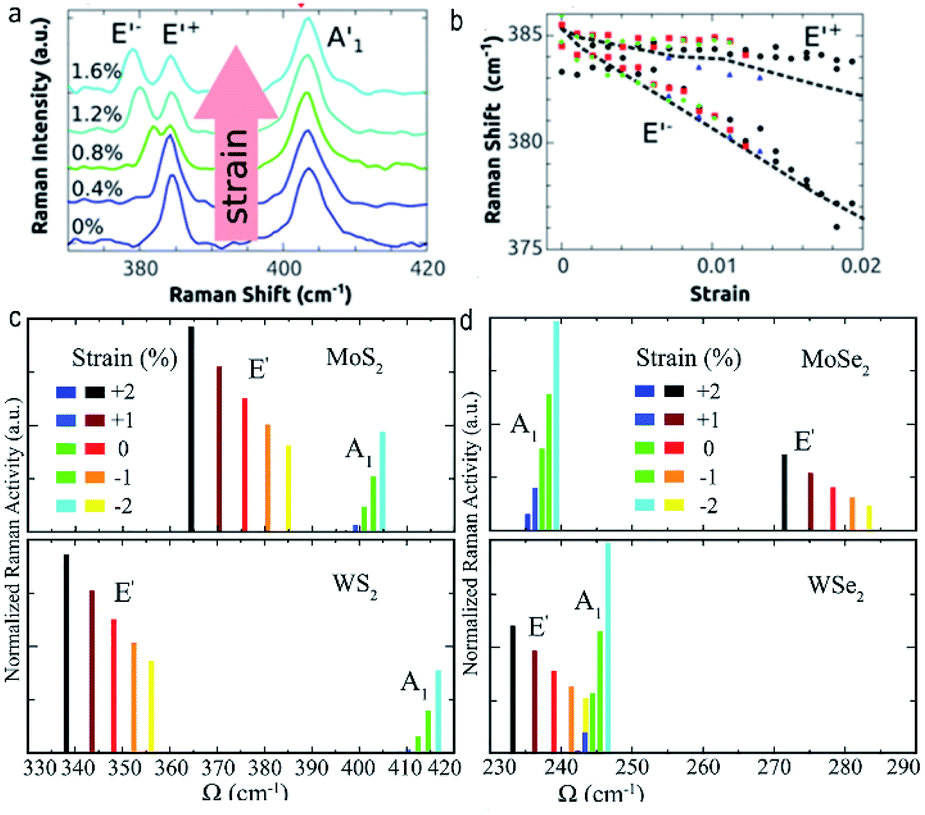 | ||
| Fig. 2 (a) Raman spectra of monolayer MoS2 under different strain. (b) Strain-dependent Raman frequency of mode E′ in monolayer MoS2. Reproduced with permission.50 Copyright 2013, American Chemical Society. The calculated strain responses of Raman activities of monolayer (c) MoS2 and WS2 and (d) MoSe2 and WSe2. Reproduced with permission.53 Copyright 2018, American Physical Society. | ||
Sometimes, strain-induced phase transition can also be observed in strained ultrathin TMDs. For example, both experimental observations and theoretical calculations have demonstrated a phase transition of monolayer MoTe2 from semiconducting 2H phase to metal 1T′ phase, once a tensile strain of 0.3% is applied in it,54,55 indicating potential applications of monolayer MoTe2 in electronic and nanoelectromechanical devices.
In addition, it is known that the heat conduction process of semi-conductive and insulated materials are mainly dependent on phonons, electrons contribute very little even at low temperature, thus, strain engineering is an effective mean to modify the thermal conductivity of semi-conductive ultrathin TMDs owing to its softening/stiffening of phonon modes upon tensile/compressive strain.56 A low lattice thermal conductivity is favored in thermoelectric57,58 and thermal rectification59 applications, while a high lattice thermal conductivity is preferred in power sources and transistors to dissipate waste heat efficiently.60 However, the influences of strain on the thermal transport properties of ultrathin 2D materials are unpredictable, since the completely opposite responses of out-of-plane acoustic (ZA) mode with the transverse acoustic (TA) and longitudinal acoustic (LA) modes upon tensile/compressive strain. In detail, upon tensile strain, the ZA mode of two-dimensional (2D) materials becomes harder whereas the TA and LA modes become softened.61 Thus, the lattice thermal conductivity of ultrathin TMDs should be directly related to the contribution percentage of ZA, TA and LA. For instance, according to the first-principles calculations and the Boltzmann transport equation (BTE), at ambient condition, for both monolayer 2H-MoTe2 and monolayer ZrTe2, the rotational symmetry of the out-of-plane mode causes a quadratic ZA modes near the high symmetric Γ point, and ZA mode is the main contributor of the lattice thermal conductivity.61,62 Whereas, as tensile strain increases, the rotational symmetry is broken, the ZA mode changes from a quadratic nature to a linear one, resulting in a decrease (increase) in the contribution from the ZA (TA/LA) mode, thus, the lattice thermal conductivity of monolayer exhibit a dramatically reduction upon tensile strain.61,62
At present, the studies on the thermal transport properties of strained ultrathin TMDs still remain on the level of theoretical calculations. The relative experiment investigations are difficult to implement due to the following reasons: (1) the large specific surface area of ultrathin TMDs should lead to a large thermal radiation, which will undoubtedly influence the experimental results of thermal conduction. (2) The introduction of strain in ultrathin TMDs is totally dependent on the substrate, the close contact between substrate and TMDs films and the intrinsic ultrathin character of TMDs film make it difficult to calibrate the temperature of TMDs films, leading to a stalling state in experimental measurements, more work should be done to obtain breakthrough progress in experimental studies.
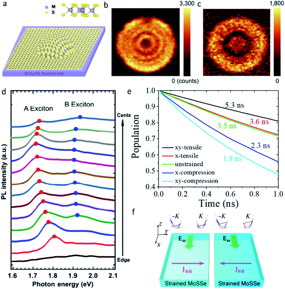 | ||
| Fig. 3 (a) Schematic diagram of a MoS2 bubble with isotropic tensile strain. PL intensity mapping images of strained MoS2 bubble at the resonant energies of (b) A excitons and (c) B excitons. (d) PL spectra of four-layer MoS2 as a function of radial coordinate over MoS2 bubble, whose center is defined as r = 0. Reproduced with permission.67 Copyright 2020, Springer. (e) Nonradiative exciton recombination dynamics of monolayer WSe2 at different strains. Reproduced with permission.68 Copyright 2019, American Chemical Society. (f) Schematic diagram of strong gate dependence of nonlinear Hall effects in strained MoSSe. Reproduced with permission.69 Copyright 2020, American Physical Society. | ||
At present, photoluminescence (PL) spectroscopy, adsorption spectroscopy, and first-principles calculations have become the mainstream methods to investigate the electronic properties of ultrathin TMDs under strain.28,50,70,71 It should be mentioned that the strain-induced electronic structural transition of ultrathin TMDs are significantly dependent on the type of strain, the type of chalcogenide atoms, and the thickness of ultrathin MX2 films. In the following statement, we will illuminate the effects of all these factors one by one.
First of all, we discuss the electronic structure of ultrathin TMDs under different types of strain. Despite the fact that both tensile strain and shear strain can induce a semiconductor-to-metal transition in ultrathin TMDs, their physical mechanisms of metallization are quite different. The tensile strain-induced metallization of group-VI TMDs monolayer can be attributed to the overlapping of px-orbitals, while the shear strain-induced metallization of group-VI TMDs monolayer results from the transition between dz2 orbitals.72
Meanwhile, although similar lattice and electronic structural evolutions can be achieved in ultrathin TMDs through uniaxial and biaxial strain, biaxial strain should be more effective in modifying the lattice and electronic structure of ultrathin TMDs when compare to uniaxial strain.44,63 For instance, a band gap transition from K–Σmin to Γ–Σmin is expected to occur at a much larger uniaxial compressive strain when compared to the biaxial compression strain.73 A semiconductor to metal transition in monolayer MX2 can be obtained more easily by application of biaxial tensile strain when compared to the uniaxial strain due to the overlapping of dz2 orbital at Fermi level.72 Moreover, a biaxial tensile strain can lead to a much larger increasing carrier mobility in monolayer MoS2 when compared to the uniaxial tensile strain.74
In addition, the strain direction should also be an important factor which can significantly influence the electronic structural evolution and electrical transport properties of ultrathin MX2. For monolayer MoS2, a uniaxial strain perpendicular to the transport axis can effectively tune the band gap of monolayer MoS2 in a wide range without changing the conductivity significantly, while a parallel strain results in a decreased band gap and a reduced conductance for the electron energies lower than the Fermi energy.44 In addition, the mobility of monolayer MoS2 is hardly affected by a tensile uniaxial strain along the zigzag direction, while it increases for tensile uniaxial strain along the armchair direction.74
Secondly, it should be mentioned that the electronic structure of ultrathin TMDs under strain are significantly sensitive to the type of chalcogens/transition metal atoms. For group-VI TMDs, less shear strain and more tensile strain is required to attain a direct-to-indirect band gap transition in heavier chalcogens owing to its diffuse nature,72 and less (more) compressive strain is needed to achieve a semiconductor-to-metal transition in heavier chalcogens (transition-metal) atoms.75 At the same strain, monolayer WS2 possesses the lightest effective mass among the group-VI TMDs MoS2, MoSe2, WS2, and WSe2,76 indicating that monolayer WS2 should be a more excellent candidate in high performance electronic devices when compared to the rest of the group-VI TMDs.
Third, the electronic structure and physical property of strained ultrathin TMDs are strongly dependent on their thickness. Influenced by the interlayer coupling and quantum confinement effect, monolayer and multilayer MX2 under tensile strain will exhibit obviously different electronic structures, optical and piezoelectric properties. An application of the uniaxial tensile strain on monolayer MX2 (M = Mo, W; X = S, Se) will lead to a redshift of photoluminescence (PL) energy thanks to the narrowed band gap, along with a reduction of the PL intensity at the K point of the Brillion zone owing to the transition from direct to indirect band gap.31,50,77–79 (Fig. 4a and b). Whereas, tensile strain can result in an enhanced PL intensity in ultrathin (2–4 layers) WS2 and WSe2 owing to the strain-induced indirect to direct bandgap transition,77,80,81 (Fig. 4c–e) which makes it promising in fabricating novel photoelectric devices. In addition, previous experimental study of the piezoelectric properties of ultrathin MoS2 confirmed that, stretching and releasing the substrate cyclically can lead to an oscillating piezoelectric voltage and current outputs in MoS2 with an odd number of atomic layers, however, this effect disappeared in MoS2 with an even number of layers, which can be attributed to the opposite orientations of adjacent atomic layers82 (Fig. 4f and g).
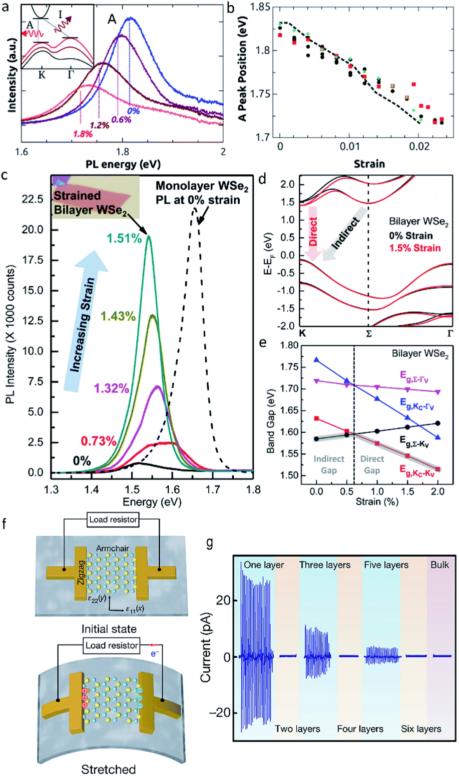 | ||
| Fig. 4 (a) The PL spectra of monolayer MoS2 under different tensile strain. (b) Energy of peak A as a function of strain. Reproduced with permission.50 Copyright 2013, American Chemical Society. (c) The PL spectra of bilayer WSe2 under different tensile strain. (d) Calculated bandgap structure of bilayer WSe2 at the strain of 0% and 1.5%. (e) Calculated bandgap energies for different transitions in bilayer WSe2 as a function of strain. Reproduced with permission.80 Copyright 2014, American Chemical Society. (f) Schematic diagram of monolayer MoS2 piezoelectric device. When the device is stretched, piezoelectric polarization charges of opposite polarity are induced at the zigzag edges of monolayer MoS2. (g) The piezoelectric outputs as a function of layer number in ultrathin MoS2. Reproduced with permission.82 Copyright 2014, Nature. | ||
It should be mentioned that the strain-induced changes of electronic structure will undoubtedly lead to the electrical transport properties evolution in ultrathin TMDs. When it comes to the electrical transport properties, we have to refer to the “effective carrier mass”. The effective carrier mass can be effectively modified by strain owing to the changes of the covalence of the bond in ultrathin MX2 upon strain,83 leading to a tunable carrier mobility since the carrier mobility is inversely proportional to the square of carrier effective mass, according to the deformation potential (DP) theory raised by Bardeen and Shockley.84 To date, many works have been reported on the simulations about the carrier mobility of ultrathin TMDs under strain. For instance, the electron mobility of monolayer MoS2 can be dramatically increased over 10 times with the biaxial strain of 9.5%.74 The mobility cut-on rate of anisotropic monolayer ReS2 can be enhanced to almost 6 times of the original value with compressive strain of 3%.85 All these studies undoubtedly pave the way for a possible application of ultrathin TMDs in electron devices since the external strain can be easily applied in TMDs films by means of specific substrate in fabrication.
The investigations of strain modified mobility of ultrathin TMDs will undoubtedly stimulated researchers to study the effect of strain on the performance of TMD based field-effect transistors. Previous density functional theory suggested that, application of tensile strain can lead to the increase of direct-current performance of monolayer-TMDs-based-double gate field-effect transistors owing to the small energy distance between K- and Q-valleys for the TMDs.86
In addition, dipole transition preference of ultrathin TMDs can be investigated from their dielectric properties, thus, the studies on the strain-induced dielectric properties of ultrathin TMDs are of great significant in fabricating nanoelectromechanical devices.66,87 According to the previous density functional theory (DFT) calculations, the dielectric properties of ultrathin TMDs are strongly dependent on the type of strain. For monolayer MoX2 (X = S, Se, Te), tensile strain showed a stronger displacement towards lower energy in the imaginary part of dielectric function when compared to compression strain, and the application of tensile strain and asymmetric biaxial strain lead to the increase of static dielectric constant, while the application of compression strains result in the first decrease and then increase of static dielectric constant.43
At present, the investigations on the electrical transport properties of ultrathin TMDs under strain are still based on the theoretical calculation. First of all, the band structure of ultrathin TMDs under strain is calculated based on the first-principles calculations, subsequently, effective mass (m*) of charge carrier is calculated according to the calculated band structure since the carrier effective mass is directly related to the energy band curvature,88 then, the carrier mobility is evaluated based on the linearized Boltzmann transport equation (BTE).89 However, it is worth mentioning that the calculated carrier mobility based on the linearized Boltzmann transport equation is imprecise since a number of factors have been ignored during the simulation of the transport processes, such as the neglect of the coherence and interaction among various particles. Thus, realizing the successful measurements of the electrical transport properties of strained ultrathin TMDs is a key issue that remains to be resolved.
The discussion above mainly focuses on the research progress and open issues about the strain-tuned electronic, optical and electrical transport properties of ultrathin TMDs. Inversely, various optical and electrical techniques have also been demonstrated to be efficient and convenient in probing strain in ultrathin TMDs. The strain imaging at submicron scale can be obtained by performing micro-Raman,48,90 absorption, photoluminescence spectroscopy,21,28,78 since both the Raman frequencies and optical band gap of ultrathin TMDs are sensitive to strain engineering (Fig. 5a–c). Furthermore, the extraction of the full strain tensor with a spatial resolution below the optical diffraction limit can be realized by performing polarization resolved second harmonic generation (SHG) measurements, based on the strain-sensitive nonlinear susceptibility tensor due to a photoelastic effect91,92 (Fig. 5d). All these optical techniques are nondestructive, allowing for large-area strain imaging with submicron spatial resolution and are simple to set up. In addition, the accurate measurement of mobility of ultrathin TMDs could also be an effective method to calibrate strain, as previous theoretical calculations predicted, the inter-valley phonon limited mobility of single layer MoSe2 and WSe2 is very sensitive to strain93 (Fig. 5e).
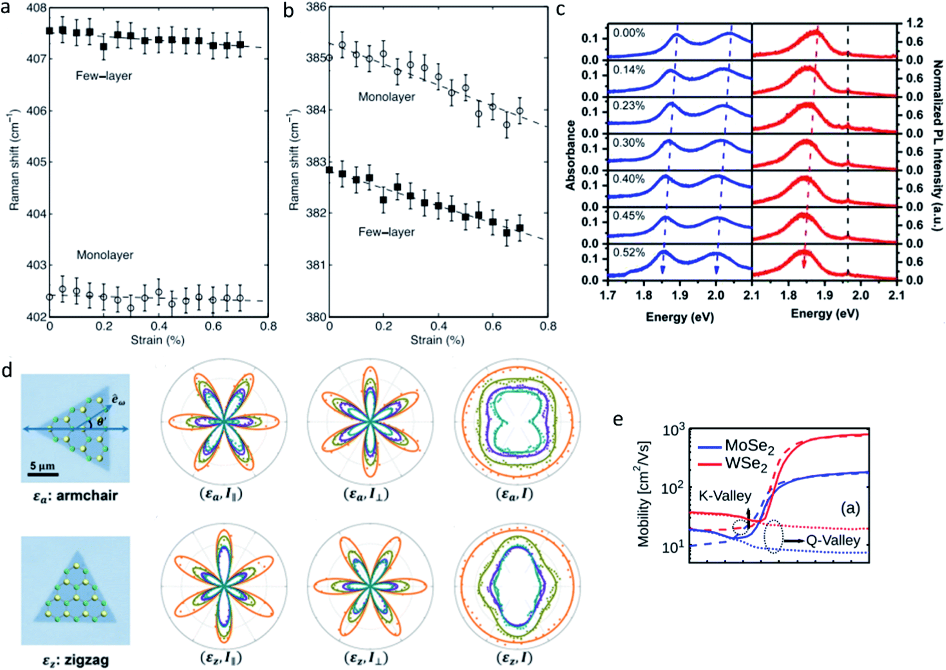 | ||
| Fig. 5 The Raman frequencies of (a) A1g and (b) E12g mode of monolayer and few layer MoS2 as a function of strain. Reproduced with permission.48 Copyright 2013, American Physical Society. (c) The absorption (left panel) and PL (right panel) spectra of monolayer MoS2 under tensile strains. Reproduced with permission.78 Copyright 2013, American Chemical Society. (d) Pattern evolution of SHG intensity for monolayer MoSe2 under strain, θ′ denote the angle between the laser excitation polarization and the strain direction. The strain magnitude is estimated from the SHG intensity, and the strain direction is judged based on the polarization-dependent SHG pattern. Reproduced with permission.92 Copyright 2017, American Chemical Society. (e) The phonon limited mobility as a function of strain in monolayer MoSe2 and WSe2. Reproduced with permission.93 Copyright 2015, American Institute of Physics. | ||
In the past decades, substantial researches about the magnetic properties of strained ultrathin TMDs have been reported, which mainly focus on the theoretical prediction of magnetic moment, magnetism order and strength of magnetic coupling under strain. Intriguing magnetization behaviors and magnetic transition have been obtained in strained ultrathin TMDs owing to their strain-induced lattice and electronic structural evolution.98–100
Despite the fact that the vast majority of TMDs are nonmagnetic at ambient condition, there also exist very rare magnetic TMDs, such as group-V TMDs VX2 (X = S, Se). It should be mentioned that their strain-induced magnetic property evolutions are strongly dependent on the types of strain. For instance, previous density functional theory suggested that, application of in-plane biaxial strain can induce a phase transition of monolayer VS2 from semiconducting-H phase to metallic-T phase, accompanied by a high spin to low spin magnetic transition.99 While application of isotropic strain can lead to increasing magnetic moments and strength of magnetic coupling in VS2 and VSe2 monolayers, the increasing magnetic moments can be attributed to the increasing bond length of dv–x, namely the increasing ionic composition of the interaction between the V and S/Se atoms, while the increasing magnetic coupling arise from the combined effects of both through-bond and through-space interactions.100
It is worth mentioning that, for intrinsically nonmagnetic ultrathin TMDs, their strain-induced magnetism are depending on not only the increasing bond lengths with strain but also the particular metallic character of ultrathin TMDs.98 That is, magnetism behaviors can be observed in strained metallic TMDs, such as group-V TMDs MX2 (M = Nb, Ta; X = S, Se), while the strained semi-conductive TMDs such as group-VI and group-X TMDs MX2 (M = Mo, W, Pt; X = S, Se) cannot be magnetized thanks to the presence of certain band gap.98,101–103 Actually, similar situations have also been observed in other 2D materials, such as Ni-substituted graphene and nanotubes where only metallic structure can be magnetized under strain.95,96
Despite the fact that strain engineering alone cannot induce magnetism in semi-conductive TMDs, combination of strain engineering with other modifications, such as doping and hydrogenation, is an effective technique to introduce and manipulate the magnetism in ultrathin group-VI TMDs thanks to the localizing unpaired 3d electrons of TM atoms and the controllable strength of the spin-splitting of TM-3d orbitals under strain. Next, the magnetic behaviors of strained semi-conductive TMDs are discussed from two aspects: doping and hydrogenation.
On the one hand, the “doping” here refers to the TM atoms embedding or the vacancies in ultrathin TMDs. Application of tensile strain can lead to magnetism in TM-atom-doped TMDs films, even magnetic transformation in TM atoms substituted TMDs, which can be attributed to the conversion from covalent to ionic bonding between TM atoms and chalcogens atoms.104,105 For instance, by application of tensile strain of 8%, a strain-induced phase transition from 2H phase to 1T phase can be obtained in the relatively low Re doping concentration in monolayer MoTe2, accompanied by a sudden magnetization phenomenon (Fig. 6a–d). In addition, the combination of vacancy doping and strain engineering can also lead to magnetism in ultrathin TMDs. Previous first-principles calculations suggested that, under tensile strain, magnetism can be introduced and manipulated in vacancies doped monolayer MoS2 owing to the breaking or the change of Mo–Mo metallic bonds around the vacancies106 (Fig. 6e).
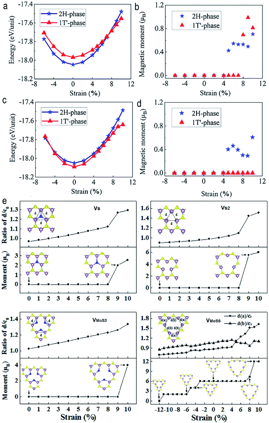 | ||
| Fig. 6 (a) Total energy and (b) magnetic moment of Mo0.9Re0.1Te2 as a function of tensile strain. (c) Total energy and (d) magnetic moment of Mo0.875Re0.125Te2 under different strain. Reproduced with permission.104 Copyright 2020, American Chemical Society. (e) Strain dependent magnetic moments for the VS, VS2, VMoS3, and VMoS6 doped monolayer MoS2. Reproduced with permission.106 Copyright 2014, American Institute of Physics. | ||
Moreover, not only the magnetism, but also the magnetization direction of ultrathin TMDs can be effectively modified by combination of doping and strain engineering. A magnetic state transition from low spin to high spin and a spin reorientation transition from out-of-plane to in-plane magnetization were predicted in strained Fe-doped monolayer MoS2.107 Similar situation were also demonstrated in strained monolayer PtSe2 with Se vacancy103 (Fig. 7).
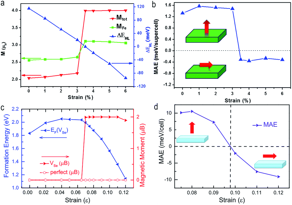 | ||
| Fig. 7 (a) Magnetic moment (vertical coordinate on the left) and the energy difference between high spin and low spin (vertical coordinate on the right) of Fe doped monolayer MoS2 as a function of strain. (b) The strain-dependent magnetocrystalline anisotropy energy (MAE) in Fe doped monolayer MoS2. Spin reorientation transition from out-of-plane to in-plane magnetization occurs when the strain is larger than 3%. Reproduced with permission.107 Copyright 2015, Elsevier. The strain-dependent (c) formation energy of VSe and total magnetic moments of Vse doped monolayer PtSe2. (d) MAE in Vse dopped monolayer PtSe2. The strain induced magnetization direction transition occurs in Vse dopped monolayer PtSe2 at the strain of 0.1%. Reproduced with permission.103 Copyright 2016, American Institute of Physics. | ||
On the other hand, using atomic hydrogen to functionalize the nonmagnetic TMDs can not only form a chemical bond easily with the chalcogens atom but also serve as an electron donor to the host, in this way, the perfect combination of hydrogenation and strain engineering will provide a great opportunity for the introduction and modification of magnetic properties in ultrathin TMDs. For instance, a strain-induced ground-state transition from nonmagnetism to ferromagnetism (FM) accompanied with enhanced magnetic moment and stability was predicted in hydrogenated MoS2 and hydrogenated MoSe2.108
At present, the magnetic properties studies of ultrathin TMDs are mainly based on the theoretical calculations, the relative experimental evidences are still scarce due to the restriction of the experimental facility. When it comes to the relatively fewer experimental observations, it should be mentioned that magnetic force microscopy (MFM) is an effective experimental facility which can be used to explore the strain-induced magnetization behaviors since it can distinguish the magnetic and nonmagnetic responses at nanometer scale.109 with the aid of MFM, Yang et al. have investigated the strain-induced magnetic property of monolayer ReSe2, where local strain was introduced on top of the wrinkled monolayer ReSe2. Magnetic phenomenon was observed at the wrinkle regions in monolayer ReSe2, evidenced by the reverse shift of the MFM phase and amplitude images. Further density functional theory also demonstrated a more stable magnetic state of strained monolayer ReSe2 when compared with the nonmagnetic states.70
It should be mentioned that, sometimes, only using theoretical calculation method to predict the magnetic behaviors of strained TMDs films may lead to controversial conclusions. For instance, Zhou et al. predicted a tensile-strain-induced magnetization with a ferromagnetic character in monolayer NbS2 and NbSe2.98 While Xu et al. predicted a tensile-strain-induced transition from antiferro- to ferro-magnetism in both monolayer NbS2 and NbSe2.110 It is obvious that this contradiction cannot be solved by just relying on the theoretical calculations, more experimental evidences are required to solve this controversy. Thus, it is time to develop the relative experimental techniques to provide more intuitive results and promote the progress of studies on the strain-induced magnetic properties of ultrathin TMDs.
Challenges and opportunities
According to the previous theoretical reports, most of the TMDs films are predicted to be capable of sustaining much larger strain when compared with their bulk counterparts, however, microcracks may appear in TMDs-based devices even at small strain, which can be attributed to the defects and the brittleness in ultrathin TMDs.111,112 Since the existence of defects, such as doping, vacancies, and grain boundaries, are inevitable during the preparation of TMDs films, it is still a great challenge to fabricate ultrathin-TMDs-based devices capable of surviving large strain.In addition, an immense amount of theoretical researches have been reported during the past decades, however, the development of experimental researches always lag behide the theoretical researches. Firstly, despite great progress has been made in the synthesis of large-area uniform TMDs films,11 the restriction of facility remains a significant problem in realizing effective modification of the thermal transport, electrical transport, and magnetic properties in strained ultrathin TMDs. Secondly, although the difference of strain-induced physical properties along the armchair and zigzag directions is small for isotropic ultrathin TMDs, there is a gap between theoretical and experimental studies on the uniaxial strain in anisotropic TMDs films. In detail, for most of the theoretical calculations and simulations, the strain effects of anisotropic TMDs films are strictly separated according to the strain directions, while when it comes to the experimental operation, the precise control of strain engineering along the armchair and zigzag direction is still difficult due to the huge challenges in exact crystallographic strain actuation and measurements. To confirm the existing prediction and reduce the distance between theory and experiment, it is time to accelerate the development of experimental technology.
Conclusions
In this review, we first focus on the experimental acheivements in approaches for introducing uniaxial, biaxial, and isotropic strain in ultrathin TMDs, the characteristics and merits of each approach have been summarized. Subsequently, the research progress in the modification of physical properties in strained ultrathin TMDs, including both experiment observations and theoretical calculations, were outlined by categorizing the physical properties: (1) lattice structure, phonon properties and thermal transport properties; (2) electronic, optical and electrical transport properties; and (3) magnetic properties. Futuristically, fabricating ultrathin-TMDs-based devices capable of surviving large strain, and trying hard to explore the experimental facilities and conditions to reduce the distance from theoretical calculations, should be the only way to achieve great success in designing TMDs based devices.Conflicts of interest
There are no conflicts to declare.Acknowledgements
This work was supported by the National Key Research and Development Program (No. 2017YFA0403704) and Jilin Engineering Normal University PhD startup foundation BSKJ201831.References
- K. S. Novoselov, A. K. Geim, S. V. Morozov, D. Jiang, Y. Zhang, S. V. Dubonos, I. V. Grigorieva and A. A. Firsov, Science, 2004, 306, 666 CrossRef CAS.
- A. Gupta, T. Sakthivel and S. Seal, Prog. Mater. Sci., 2015, 73, 44 CrossRef CAS.
- K. Khan, A. K. Tareen, M. Aslam, R. Wang, Y. Zhang, A. Mahmood, Z. Ouyang, H. Zhang and Z. Guo, J. Mater. Chem. C, 2020, 8, 387 RSC.
- M. Chhowalla, H. S. Shin, G. Eda, L. J. Li, K. P. Loh and H. Zhang, Nat. Chem., 2013, 5, 263 CrossRef.
- R. Vargas-Bernal, Sensors, 2019, 19, 1295 CrossRef CAS.
- M. Holwill, Nanomechanics in van der Waals Heterostructures, 2019, 2, 7 CrossRef.
- E. Singh, P. Singh, K. S. Kim, G. Y. Yeom and H. S. Nalwa, ACS Appl. Mater. Interfaces, 2019, 11, 11061 CrossRef CAS.
- N. Huo, Y. Yang and J. Li, J. Semicond., 2017, 38, 031002 CrossRef.
- Q. H. Wang, K. Kalantar-Zadeh, A. Kis, J. N. Coleman and M. S. Strano, Nat. Nanotechnol., 2012, 7, 699 CrossRef CAS.
- K. Zhang, Y. C. Lin and J. A. Robinson, Semicond. Semimetals, 2016, 95, 189 CAS.
- A. Zavabeti, A. Jannat, L. Zhong, A. A. Haidry, Z. Yao and J. Z. Ou, Nano-Micro Lett., 2020, 12, 66 CrossRef CAS.
- W. Choi, N. Choudhary, G. H. Han, J. Park, D. Akinwande and Y. H. Lee, Mater. Today, 2017, 20, 116 CrossRef CAS.
- J. Pu, Y. Yomogida, K. K. Liu, L. J. Li, Y. Iwasa and T. Takenobu, Nano Lett., 2012, 12, 4013 CrossRef CAS.
- A. Castellanos-Gomez, M. Poot, G. A. Steele, H. S. van der Zant, N. Agrait and G. Rubio-Bollinger, Adv. Mater., 2012, 24, 772 CrossRef CAS.
- S. Bertolazzi, J. Brivio and A. Kis, ACS Nano, 2011, 5, 9703 CrossRef CAS.
- Z. Dai, L. Liu and Z. Zhang, Adv. Mater., 2019, 31, 1805417 CrossRef CAS.
- Y. Sun and K. Liu, J. Appl. Phys., 2019, 125, 082402 CrossRef.
- R. Roldán, A. Castellanos-Gomez, E. Cappelluti and F. Guinea, J. Phys.: Condens. Matter, 2015, 27, 313201 CrossRef.
- C. R. Zhu, G. Wang, B. L. Liu, X. Marie, X. F. Qiao, X. Zhang, X. X. Wu, H. Fan, P. H. Tan, T. Amand and B. Urbaszek, Phys. Rev. B: Condens. Matter Mater. Phys., 2013, 88, 121301 CrossRef.
- A. M. Dadgar, D. Scullion, K. Kang, D. Esposito, E. H. Yang, I. P. Herman, M. A. Pimenta, E. J. G. Santos and A. N. Pasupathy, Chem. Mater., 2018, 30, 5148 CrossRef CAS.
- A. Castellanos-Gomez, R. Roldan, E. Cappelluti, M. Buscema, F. Guinea, H. S. van der Zant and G. A. Steele, Nano Lett., 2013, 13, 5361 CrossRef CAS.
- H. Li, A. W. Contryman, X. Qian, S. M. Ardakani, Y. Gong, X. Wang, J. M. Weisse, C. H. Lee, J. Zhao, P. M. Ajayan, J. Li, H. C. Manoharan and X. Zheng, Nat. Commun., 2015, 6, 7381 CrossRef CAS.
- M. G. Harats, J. N. Kirchhof, M. Qiao, K. Greben and K. I. Bolotin, Nat. Photonics, 2020, 14, 324–329 CrossRef CAS.
- F. A. Benimetskiy, V. A. Sharov, P. A. Alekseev, V. Kravtsov, K. B. Agapev, I. S. Sinev, I. S. Mukhin, A. Catanzaro, R. G. Polozkov, E. M. Alexeev, A. I. Tartakovskii, A. K. Samusev, M. S. Skolnick, D. N. Krizhanovskii, I. A. Shelykh and I. V. Iorsh, APL Mater., 2019, 7, 101126 CrossRef.
- J. Qi, Y.-W. Lan, A. Z. Stieg, J.-H. Chen, Y.-L. Zhong, L.-J. Li, C.-D. Chen, Y. Zhang and K. L. Wang, Nat. Commun., 2015, 6, 7430 CrossRef CAS.
- S. Manzeli, A. Allain, A. Ghadimi and A. Kis, Nano Lett., 2015, 15, 5330–5335 CrossRef CAS.
- G. Plechinger, A. Castellanos-Gomez, M. Buscema, H. S. J. v. d. Zant, G. A Steele, A. Kuc, T. Heine, C. Schüller and T. Korn, 2D Mater., 2015, 2, 015006 CrossRef.
- Y. Y. Hui, X. Liu, W. Jie, N. Y. Chan, J. Hao, Y.-T. Hsu, L.-J. Li, W. Guo and S. P. Lau, ACS Nano, 2013, 7, 7126 CrossRef CAS.
- R. Yang, J. Lee, S. Ghosh, H. Tang, R. M. Sankaran, C. A. Zorman and P. X.-L. Feng, Nano Lett., 2017, 17, 4568 CrossRef CAS.
- Y. Chen, F. Ke, P. Ci, C. Ko, T. Park, S. Saremi, H. Liu, Y. Lee, J. Suh, L. W. Martin, J. W. Ager, B. Chen and J. Wu, Nano Lett., 2017, 17, 194–199 CrossRef CAS.
- Y. Wang, C. Cong, W. Yang, J. Shang, N. Peimyoo, Y. Chen, J. Kang, J. Wang, W. Huang and T. Yu, Nano Res., 2015, 8, 2562–2572 CrossRef CAS.
- V. S. Mangu, M. Zamiri, S. R. J. Brueck and F. Cavallo, Nanoscale, 2017, 9, 16602 RSC.
- H. Li, C. Tsai, A. L. Koh, L. Cai, A. W. Contryman, A. H. Fragapane, J. Zhao, H. S. Han, H. C. Manoharan, F. Abild-Pedersen, J. K. Norskov and X. Zheng, Nat. Mater., 2016, 15, 48 CrossRef CAS.
- H. Li, M. Du, M. J. Mleczko, A. L. Koh, Y. Nishi, E. Pop, A. J. Bard and X. Zheng, J. Am. Chem. Soc., 2016, 138, 5123 CrossRef CAS.
- E. Khestanova, F. Guinea, L. Fumagalli, A. K. Geim and I. V. Grigorieva, Nat. Commun., 2016, 7, 12587 CrossRef CAS.
- K. S. Vasu, E. Prestat, J. Abraham, J. Dix, R. J. Kashtiban, J. Beheshtian, J. Sloan, P. Carbone, M. Neek-Amal, S. J. Haigh, A. K. Geim and R. R. Nair, Nat. Commun., 2016, 7, 12168 CrossRef CAS.
- H. Yoshida, V. Kaiser, B. Rotenberg and L. Bocquet, Nat. Commun., 2018, 9, 1496 CrossRef.
- G. Zamborlini, M. Imam, L. L. Patera, T. O. Mentes, N. Stojic, C. Africh, A. Sala, N. Binggeli, G. Comelli and A. Locatelli, Nano Lett., 2015, 15, 6162 CrossRef CAS.
- D. Lloyd, X. Liu, J. W. Christopher, L. Cantley, A. Wadehra, B. L. Kim, B. B. Goldberg, A. K. Swan and J. S. Bunch, Nano Lett., 2016, 16, 5836–5841 CrossRef CAS.
- H. Luo, X. Li, Y. Zhao, R. Yang, L. Bao, Y. Hao, Y. Gao, N. N. Shi, Y. Guo, G. Liu, L. Zhao, Q. Wang, Z. Zhang, G. Zhang, J. Sun, Y. Huang, H. Gao and X. Zhou, Phys. Rev. Mater., 2020, 4, 074006 CrossRef CAS.
- A. V. Tyurnina, D. A. Bandurin, E. Khestanova, V. G. Kravets, M. Koperski, F. Guinea, A. N. Grigorenko, A. K. Geim and I. V. Grigorieva, ACS Photonics, 2019, 6, 516–524 CrossRef CAS.
- A. P. Nayak, T. Pandey, D. Voiry, J. Liu, S. T. Moran, A. Sharma, C. Tan, C.-H. Chen, L.-J. Li, M. Chhowalla, J.-F. Lin, A. K. Singh and D. Akinwande, Nano Lett., 2015, 15, 346–353 CrossRef CAS.
- A. Kumar and P. K. Ahluwalia, Phys. B, 2013, 419, 66 CrossRef CAS.
- M. Ghorbani-Asl, S. Borini, A. Kuc and T. Heine, Phys. Rev. B: Condens. Matter Mater. Phys., 2013, 87, 235434 CrossRef.
- S.-D. Guo and Y. Wang, Semicond. Sci. Technol., 2017, 32, 055004 CrossRef.
- Q. Zhang, Z. Chang, G. Xu, Z. Wang, Y. Zhang, Z.-Q. Xu, S. Chen, Q. Bao, J. Z. Liu, Y.-W. Mai, W. Duan, M. S. Fuhrer and C. Zheng, Adv. Funct. Mater., 2016, 26, 8707 CrossRef CAS.
- Q. Zhang, Y. Cheng, L.-Y. Gan and U. Schwingenschlögl, Phys. Rev. B: Condens. Matter Mater. Phys., 2013, 88, 245447 CrossRef.
- C. Rice, R. J. Young, R. Zan, U. Bangert, D. Wolverson, T. Georgiou, R. Jalil and K. S. Novoselov, Phys. Rev. B: Condens. Matter Mater. Phys., 2013, 87, 081307 CrossRef.
- A. McCreary, R. Ghosh, M. Amani, J. Wang, K. A. N. Duerloo, A. Sharma, K. Jarvis, E. J. Reed, A. M. Dongare, S. K. Banerjee, M. Terrones, R. R. Namburu and M. Dubey, ACS Nano, 2016, 10, 3186 CrossRef CAS.
- H. J. Conley, B. Wang, J. I. Ziegler, R. F. Haglund Jr, S. T. Pantelides and K. I. Bolotin, Nano Lett., 2013, 13, 3626 CrossRef CAS.
- Y. Wang, C. Cong, C. Qiu and T. Yu, Small, 2013, 9, 2857 CrossRef CAS.
- E. Scalise, M. Houssa, G. Pourtois, V. V. Afanas'ev and A. Stesmans, Phys. E, 2014, 56, 416 CrossRef CAS.
- M. Yagmurcukardes, C. Bacaksiz, E. Unsal, B. Akbali, R. T. Senger and H. Sahin, Phys. Rev. B, 2018, 97, 115427 CrossRef CAS.
- S. Song, D. H. Keum, S. Cho, D. Perello, Y. Kim and Y. H. Lee, Nano Lett., 2016, 16, 188 CrossRef CAS.
- K.-A. N. Duerloo, Y. Li and E. J. Reed, Nat. Commun., 2014, 5, 4214 CrossRef CAS.
- S. Bhowmick and V. B. Shenoy, J. Chem. Phys., 2006, 125, 164513 CrossRef.
- J. R. Sootsman, D. Y. Chung and M. G. Kanatzidis, Angew. Chem., Int. Ed., 2009, 48, 8616 CrossRef CAS.
- J. R. Szczech, J. M. Higgins and S. Jin, J. Mater. Chem., 2011, 21, 4037 RSC.
- M. Hu, P. Keblinski and B. Li, Appl. Phys. Lett., 2008, 92, 211908 CrossRef.
- W. K. CHAN, Jpn. J. Appl. Phys., 1998, 37, 813 CrossRef CAS.
- A. Shafique and Y. H. Shin, Phys. Chem. Chem. Phys., 2017, 19, 32072 RSC.
- R. D'Souza, S. Mukherjee and S. Ahmad, J. Appl. Phys., 2019, 126, 214302 CrossRef.
- Z. Khatibi, M. Feierabend, M. Selig, S. Brem, C. Linderälv, P. Erhart and E. Malic, 2D Mater., 2019, 6, 015015 CrossRef CAS.
- X. Liu, H. Zhou, B. Yang, Y. Qu and M. Zhao, Sci. Rep., 2017, 7, 39995 CrossRef CAS.
- M. Feierabend, A. Morlet, G. Berghäuser and E. Malic, Phys. Rev. B, 2017, 96, 045425 CrossRef.
- J. Guo, C. Ke, Y. Wu and J. Kang, Nanoscale Res. Lett., 2020, 15, 97 CrossRef CAS.
- Y. Guo, B. Li, Y. Huang, S. Du, C. Sun, H. Luo, B. Liu, X. Zhou, J. Yang, J. Li and C. Gu, Nano Res., 2020, 13, 2072 CrossRef CAS.
- Y. Yang, W. H. Fang, A. V Benderskii, R. Long and O. V. Prezhdo, J. Phys. Chem. Lett., 2019, 10, 7732 CrossRef CAS.
- B. T. Zhou, C.-P. Zhang and K. T. Law, Phys. Rev. Appl., 2020, 13, 024053 CrossRef CAS.
- S. Yang, C. Wang, H. Sahin, H. Chen, Y. Li, S. S. Li, A. Suslu, F. M. Peeters, Q. Liu, J. Li and S. Tongay, Nano Lett., 2015, 15, 1660 CrossRef CAS.
- P. Lu, X. Wu, W. Guo and X. C. Zeng, Phys. Chem. Chem. Phys., 2012, 14, 13035 RSC.
- P. Johari and V. B. Shenoy, ACS Nano, 2012, 6, 5449 CrossRef CAS.
- L. Dong, A. M. Dongare, R. R. Namburu, T. P. O'Regan and M. Dubey, Appl. Phys. Lett., 2014, 104, 053107 CrossRef.
- M. Hosseini, M. Elahi, M. Pourfath and D. Esseni, J. Phys. D: Appl. Phys., 2015, 48, 375104 CrossRef.
- S. Bhattacharyya and A. K. Singh, Phys. Rev. B: Condens. Matter Mater. Phys., 2012, 86, 075454 CrossRef.
- H. Shi, H. Pan, Y.-W. Zhang and B. I. Yakobson, Phys. Rev. B: Condens. Matter Mater. Phys., 2013, 87, 155304 CrossRef.
- K. P. Dhakal, S. Roy, H. Jang, X. Chen, W. S. Yun, H. Kim, J. Lee, J. Kim and J.-H. Ahn, Chem. Mater., 2017, 29, 5124 CrossRef CAS.
- K. He, C. Poole, K. F. Mak and J. Shan, Nano Lett., 2013, 13, 2931 CrossRef CAS.
- S. Aas and C. Bulutay, Opt. Express, 2018, 26, 28672 CrossRef CAS.
- S. B. Desai, G. Seol, J. S. Kang, H. Fang, C. Battaglia, R. Kapadia, J. W. Ager, J. Guo and A. Javey, Nano Lett., 2014, 14, 4592 CrossRef CAS.
- W. Wu, J. Wang, P. Ercius, N. C. Wright, D. M. Leppert-Simenauer, R. A. Burke, M. Dubey, A. M. Dogare and M. T. Pettes, Nano Lett., 2018, 18, 2351 CrossRef CAS.
- W. Wu, L. Wang, Y. Li, F. Zhang, L. Lin, S. Niu, D. Chenet, X. Zhang, Y. Hao, T. F. Heinz, J. Hone and Z. L. Wang, Nature, 2014, 514, 470 CrossRef CAS.
- B. Falabretti and J. Robertson, J. Appl. Phys., 2007, 102, 123703 CrossRef.
- J. Bardeen and W. Shockley, Phys. Rev., 1950, 80, 72 CrossRef CAS.
- Z. H. Zhou, B. C. Wei, C. Y. He, Y. M. Min, C. H. Chen, L. Z. Liu and X. L. Wu, Appl. Surf. Sci., 2017, 404, 276 CrossRef CAS.
- M. Hosseini and H. Karami, J. Comput. Electron., 2018, 17, 1603 CrossRef CAS.
- S. Deng, L. Li and Y. Zhang, ACS Appl. Nano Mater., 2018, 1, 1932 CrossRef CAS.
- S. Yu, H. D. Xiong, K. Eshun, H. Yuan and Q. Li, Appl. Surf. Sci., 2015, 325, 27 CrossRef CAS.
- A. Paussa and D. Esseni, J. Appl. Phys., 2013, 113, 093702 CrossRef.
- T. M. G. Mohiuddin, A. Lombardo, R. R. Nair, A. Bonetti, G. Savini, R. Jalil, N. Bonini, D. M. Basko, C. Galiotis, N. Marzari, K. S. Novoselov, A. K. Geim and A. C. Ferrari, Phys. Rev. B: Condens. Matter Mater. Phys., 2009, 79, 205433 CrossRef.
- L. Mennel, M. M. Furchi, S. Wachter, M. Paur, D. K. Polyushkin and T. Mueller, Nat. Commun., 2018, 9, 516 CrossRef.
- J. Liang, J. Zhang, Z. Li, H. Hong, J. Wang, Z. Zhang, X. Zhou, R. Qiao, J. Xu, P. Gao, Z. Liu, Z. Liu, Z. Sun, S. Meng, K. Liu and D. Yu, Nano Lett., 2017, 17, 7539 CrossRef CAS.
- M. Hosseini, M. Elahi, M. Pourfath and D. Esseni, Appl. Phys. Lett., 2015, 107, 253503 CrossRef.
- B. Huang, J. Yu and S.-H. Wei, Phys. Rev. B: Condens. Matter Mater. Phys., 2011, 84, 075415 CrossRef.
- E. J. G. Santos, A. Ayuela, S. B. Fagan, J. Mendes Filho, D. L. Azevedo, A. G. Souza Filho and D. Sánchez-Portal, Phys. Rev. B: Condens. Matter Mater. Phys., 2008, 78, 195420 CrossRef.
- E. J. G. Santos, A. Ayuela and D. Sánchez-Portal, J. Phys. Chem. C, 2012, 116, 1174 CrossRef CAS.
- C. Ataca, S. Cahangirov, E. Durgun, Y. R. Jang and S. Ciraci, Phys. Rev. B: Condens. Matter Mater. Phys., 2008, 77, 214413 CrossRef.
- Y. Zhou, Z. Wang, P. Yang, X. Zu, L. Yang, X. Sun and F. Gao, ACS Nano, 2012, 6, 9727 CrossRef CAS.
- M. Kan, B. Wang, Y. H. Lee and Q. Sun, Nano Res., 2015, 8, 1348 CrossRef CAS.
- Y. Ma, Y. Dai, M. Guo, C. Niu, Y. Zhu and B. Huang, ACS Nano, 2012, 6, 1695 CrossRef CAS.
- S. Kansara, S. K. Gupta and Y. Sonvane, Comput. Mater. Sci., 2018, 141, 235 CrossRef CAS.
- P. Manchanda, V. Sharma, H. Yu, D. J. Sellmyer and R. Skomski, Appl. Phys. Lett., 2015, 107, 032402 CrossRef.
- W. Zhang, H. T. Guo, J. Jiang, Q. C. Tao, X. J. Song, H. Li and J. Huang, J. Appl. Phys., 2016, 120, 013904 CrossRef.
- Y. Zhao, Y. Li, M. Liu, K. Xu and F. Ma, J. Phys. Chem. C, 2020, 124, 4299 CrossRef CAS.
- Y. Miao, H. Bao, W. Fan and F. Ma, J. Phys. Chem. Solids, 2020, 142, 109459 CrossRef CAS.
- H. Zheng, B. Yang, D. Wang, R. Han, X. Du and Y. Yan, Appl. Phys. Lett., 2014, 104, 132403 CrossRef.
- Z. Chen, J. He, P. Zhou, J. Na and L. Z. Sun, Comput. Mater. Sci., 2015, 110, 102 CrossRef CAS.
- H. Shi, H. Pan, Y.-W. Zhang and B. I. Yakobson, Phys. Rev. B: Condens. Matter Mater. Phys., 2013, 88, 205305 CrossRef.
- H. Li, X. Qi, J. Wu, Z. Zeng, J. Wei and H. Zhang, ACS Nano, 2013, 7, 2842 CrossRef CAS.
- Y. Xu, X. Liu and W. Guo, Nanoscale, 2014, 6, 12929 RSC.
- D. Akinwande, N. Petrone and J. Hone, Nat. Commun., 2014, 5, 5678 CrossRef CAS.
- J. H. Kim, J. H. Jeong, N. Kim, R. Joshi and G.-H. Lee, J. Phys. D: Appl. Phys., 2019, 52, 083001 CrossRef.
| This journal is © The Royal Society of Chemistry 2020 |