
 Open Access Article
 This Open Access Article is licensed under a
 Creative Commons Attribution 3.0 Unported Licence
Intriguing electronic structure and photocatalytic performance of blueP–SMSe and blueP–SeMS (M = Mo, W) van der Waals heterostructures
S. Ahmada,
Iftikhar Ahmadab,
N. Van c and
B. Amin*d
c and
B. Amin*d
aDepartment of Physics, University of Malakand, Chakdara, 18800, Pakistan
bGomal University, 29220, DI Khan, Pakistan
cInstitute of Research and Development, Duy Tan University, Da Nang 550000, Vietnam
dDepartment of Physics, Abbottabad University of Science & Technology, Abbottabad 22010, Pakistan. E-mail: binukhn@gmail.com
First published on 15th October 2020
Abstract
Van der Waals (vdW) combination of two dimensional (2D) materials in the form of a heterostructure is a widely accepted tool for tailoring properties and designing novel nanoelectronic and energy harvesting applications. The stacking geometry and electronic and photocatalytic properties of vdW heterostructures based on blueP and Janus SMSe and SeMS (M = Mo, W) monolayers are investigated by using first principles calculations. Two alternate stacking configurations of both heterostructures with an alternative order of chalcogen atoms in SMSe and SeMS (M = Mo, W) are constructed and found to be energetically and thermally stable. The feasible stackings of both heterostructures exhibit type-II band alignment (except blueP–SeMoS), hence are promising for light detection devices. In particular, the suitable positions of the valence and conduction band edges of all the heterostructures (except blueP–SMoSe) are appropriate for standard redox potentials and are capable of splitting water into O2/H2O and H+/H2. The findings pave the way for potential applications of these heterobilayer systems in future nanoelectronics, optoelectronics and photocatalytic water dissociation.
1 Introduction
The family of two-dimensional (2D) materials has been widely expanded to a variety of materials like transition metal dichalcogenides (TMDC),1–4 hexagonal boron nitrides (h-BN),5,6 phosphorene,7,8 and MXene.9,10 For instance, TMDC with the general formula MX2 (M = Mo, W; X = S, Se, Te) possess a semiconducting band gap nature, and have been extensively studied for versatile devices in optoelectronics, nanoelectronics and valleytronics.11–13 Very recently, Janus TMDC monolayers (with general formula MXY or XMY (M = Mo, W; X/Y = S, Se)) have been synthesized by breaking the structural symmetry of chalcogen atoms in MX2 through chemical vapor deposition (CVD) method.14 Janus XMY monolayers have an asymmetric structure, and exhibit a direct semiconducting band gap nature, giant Rashba spin splitting, exciting optoelectronic properties and photocatalysis of water.15–18Blue phosphorus (blueP) and black phosphorus (blackP) with buckled honeycomb lattice symmetry have also been theoretically demonstrated as new 2D allotropes of phosphorous poly-types.19–22 Zhang et al.23 have successfully synthesized single layer blueP on an Au(111) substrate using molecular beam epitaxy technique. The graphene-like single layer buckled blueP has a flatter layer than puckered black phosphorus (blackP) and is predicted to exhibit a tunable band gap (2 eV) and electronic mobility (4.6 × 10²/4.7 × 101 cm2 v−1 s−1 along armchair/zigzag directions at room temperature).24,25 Band gap engineering under external strain and electric field and the high charge capacities of single layer blueP have attracted a great deal of interest in nanoelectronics and capability for rechargeable Li-ion batteries.26
The combination of 2D materials via weak van der Waals (vdW) interactions to form heterostructures offers a way to study the controlled generation, combination or transportation of charge carriers for unique electronic, low power and ultrathin flexible photoelectronic devices.27–29 In vdW heterostructures, three different types of band alignments including type-I (symmetric), type-II (staggered), or type-III (broken) may be obtained for versatile device applications.28–30 However, heterostructures of type-II band alignment with conduction band minima (CBM) and valence band maxima (VBM) localized in two separate components lead to creation of interlayer optical excitations and reducing charge recombination rate in designing solar cells, novel optoelectronic and photovoltaic devices.31 A large variety of vdW heterostructures such as P/ZnO(SiC)31 and P/BSe32 with promising optoelectronic and photocatalytic water splitting properties have been theoretically and experimentally reported. Theoretical findings have revealed type-II band alignment with enhanced optoelectronic, spintronic and photocatalytic water splitting behavior in MoSSe/WSSe, GeC/Janus-TMDC and ZnO/Janus-TMDC heterostructures.33–35
In view of the above remarkable properties and acceptable lattice mismatch of blueP and Janus SMSe and SeMS (M = Mo, W) monolayers, the intriguing physical properties of the blueP–SMSe and blueP–SeMS (M = Mo, W) vdW stacking are investigated by first principles studies. In the present work, two different models of vdW heterostructures are formed with interchanging positions of the chalcogen atoms at the lower/top layers of the Janus monolayer. Each model has three possible stacking configurations. The feasible stacking configurations of the studied models of the heterostructures are found to be energetically and thermally stable. A detailed study of band structure, planar averaged charge density and photocatalytic behavior of the feasible stackings is carried out. Both heterostructures show type-II (except blueP–SeMoS) band alignment and are found most suitable for photocatalytic behavior. The findings reveal very promising applications of creating heterostructures for engineering optoelectronic and photovoltaic devices.
2 Computational details
Density functional theory (DFT) based calculations are performed using the projector plane wave (PAW) method36 as implemented in Vienna ab initio simulation package (VASP).37,38 DFT fails to include expansion caused by free energy of the system, hence structural comparison with systems at low temperature should make the minimum energy structure calculated by DFT+D (whatever dispersion correction) seem over-bound. Grimme DFT-D2 works best, providing the most binding out of the corrections. Therefore, vdW interactions are taken into account using the Grimme DFT-D2 method.39 The exchange-correlation functional proposed by Perdew–Burke–Ernzerhof (PBE)40 is used. In addition, the HSE06 (Heyd–Scuseria–Ernzerhof) functional is also adopted to obtain a better band gap value.41 The vacuum along the z-axis is set as 20 Å and the energy cutoff is chosen as 400 eV. The geometric relaxation is performed until the force and energy are converged to 0.001 eV Å−1 and 10−4 eV, respectively. A 6 × 6 × 1 k-point mesh is chosen for geometry relaxation and a 12 × 12 × 1 k-grid is further used for electronic structure calculations.3 Results and discussion
After performing geometrical relaxation, the calculated lattice constant (bond length) of 2D blueP is 3.27 Å (2.25 Å for P–P), of SMSe is 3.26 Å (2.42 Å for S–M (M = Mo, W)), and of SWSe is 3.26 Å (2.53 Å for Se–M (M = Mo, W)) and are in good agreement with previous work.14,24,29 This indicates the accuracy of our computational approach. BlueP, SMSe and SeMS (M = Mo, W) layers have small lattice mismatches and identical hexagonal lattices thus attaining possible direction for experimental fabrication of blueP–SMSe and blueP–SeMS (M = Mo, W) vdW heterostructures in semiconductor applications.Generally, the interfacial characteristics are sensitive to the local configuration and specified intercontacted atoms. Two different surfaces are possible for the construction of vdW heterostructures of blueP and single layer SMSe and SeMS (M = Mo, W). Therefore, two dissimilar models with interchanging positions of S and Se atoms on the opposite faces of Janus monolayer (SMSe and SeMS) were used forming three different possible stacking configurations, as shown in Fig. 1(a–c) and (d–f). In stacking a and stacking d, each blueP atom is set below the Mo, W atom and chalcogen atom. In stacking b and stacking e, one blueP atom is fixed below the chalcogen atom and a second blueP atom is placed at the hollow site. In stacking c and stacking f, an individual blueP atom is located below the Mo/W atom and another P atom occupies the hollow site.
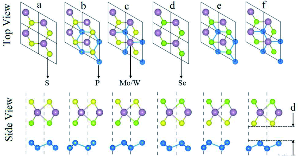 | ||
| Fig. 1 Top and side views of both models (P–SeMo(W)S and P–SMo(W)Se) with Se (a–c) and S (d–f) atoms located at the bottom surface of the Mo(W)SSe layer (details in text), and “d” represents the interlayer spacing. | ||
The binding energy of the heterobilayer system can be defined as Eb = EblueP–SMSe,blueP–SeMS − EblueP − ESMSe,SeMS, where EblueP–SMSe,blueP–SeMS represents the total energy of the blueP–SMSe, blueP–SeMS heterostructure, EblueP is the energy of the isolated single blueP layer and ESMSe,SeMS represents the total energy of SMSe, SeMS monolayers. The theoretically predicted binding energy (Eb), interlayer distance (d-spacing), optimized lattice constant (a), bond lengths (P–Mo, W and P–S, Se) of the studied heterostructures are presented in Table 1. The stacking patterns [configurations (b and e) of both models] exhibit very small interlayer spaces, which indicate highly energetic stability with very strong physical connection between blueP and MoSSe, WSSe. It is significant that the larger the covalent radius between S and Se, the larger the vdW attraction energy will be, which results in a very tiny change in the interlayer spacing. From Table 1, the smaller vertical distance “d-spacing” indicates that these heterobilayers contain vdW interactions. In addition, ab initio molecular dynamics (MD) calculations are performed to investigate the thermal stability of the studied heterobilayers. From Fig. 2, it is clear that no bond breaking or considerable variations in structure of these heterostructures is observed within 6 ps at room temperature. This indicates that all heterobilayers have stable geometry even at room temperature. Similar results are also observed in two dimensional graphene–gold interfaces.42
| Material | P–SeMoS | P–SMoSe | P–SeWS | P–SWSe |
|---|---|---|---|---|
| a (Å) | 3.26 | 3.26 | 3.27 | 3.27 |
| P–P (Å) | 2.25 | 2.25 | 2.25 | 2.25 |
| Se–Mo/W (Å) | 2.53 | 2.53 | 2.53 | 2.53 |
| S–Mo/W (Å) | 2.42 | 2.42 | 2.24 | 2.24 |
| Eb/dspacing (Å) | −0.325/3.15 | −0.325/3.17 | −0.348/3.25 | −0.347/3.24 |
| Eg-PBE (eV) | 1.02 | 0.93 | 0.92 | 0.90 |
| Eg-HSE06 (eV) | 1.82 | 1.30 | 1.62 | 1.60 |
| EVB (eV) | 1.74 | 1.58 | 1.60 | 1.59 |
| ECB (eV) | −0.084 | 0.076 | −0.25 | −0.013 |
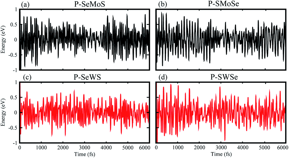 | ||
| Fig. 2 Thermal stability of P–SeMo(W)S and P–SMo(W)Se vdW heterostructures. | ||
Using both PBE and HSE06 functionals, blueP is found to be an indirect band gap semiconductor with the conduction band minimum (CBM) at the Γ–K-point and the valence band maximum (VBM) at the M–Γ-point of the Brillouin zone (BZ). The SMSe and SeMS are direct band gap semiconductors with both the CBM and VBM at the K-point of the BZ. The obtained PBE (HSE06) level band gap value for blueP is 2.19 (3.11) eV, for SMoSe is 1.47 (2.07) eV and for SWSe is 1.37 (2.07) eV. These results are in good agreement with previous literature.14,24,29 From Fig. 3, it is clear that blueP–SeMoS(blueP–SMoSe) and blueP–SeWS(blueP–SWSe) stackings possess indirect band gaps with the CBM lying between M–Γ(K) and the VBM at the K(K)-point of BZ. Band gap values of the reported vdW heterostructures are smaller than both monolayers, indicating that the formation of the vdW heterostructure reduces the band gap value. However, it is still larger than the minimum (1.23 eV) that is required for photocatalysis reactions, showing the potential application of the blueP/BSe heterostructure as a visible light photocatalyst.43
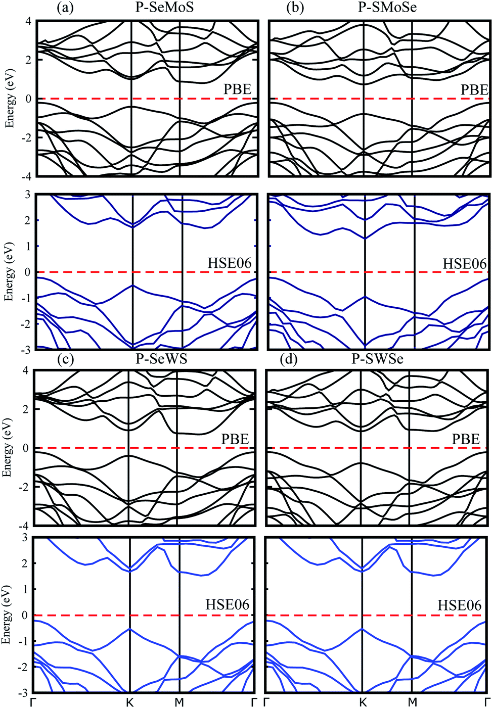 | ||
| Fig. 3 Electronic band structure of P–SeMo(W)S (a and c) and P–SMo(W)Se (b and d) with PBE (black) and HSE06 (blue) calculations. | ||
Furthermore, careful observations have been made of the band alignments of blueP, SMSe, and SeMS vdW heterostructures by plotting the projected weighted bands, as shown in Fig. 4. Obviously, the P-pz orbital mainly contributes in the VBM and the Mo-dz2 (W-dxy) orbital dominates the CBM in P–SMoSe and P–SeWS and P–SWSe. Certainly, the CBM and VBM in blueP–SMoSe, and blueP–SWSe are confined in blueP and SMoSe, SWSe monolayers, clearly showing type-II band alignment (known as staggered type). The VBM and CBM are localized from the Janus monolayers and blueP monolayer, respectively at the interface between these two layers. Such a type-II band-alignment spontaneously separates electrons and holes, enabling high efficiency optoelectronics and solar energy conversions.43–46 It has been discovered that type-II band alignments are mostly crucial in carrier separation of charges. This trend has been found in MoSSe–WSSe, GeC/Janus-TMDCs, ZnO/Janus-TMDCs, and SiC-TMDCs.33–35 Apparently, photogenerated electrons will transfer from blueP to SMoSe, SWSe and holes will move in the opposite direction from SMoSe, SWSe to blueP, this mechanism will minimize the rate of combination of charge. Hence, blueP–SMoSe, blueP–SWSe heterostructures must be thoroughly considered for applications in solar cells.47 However, the VBM and CBM are dominated by the Mo-dz2 orbital in P–SeMoS indicating type-I band alignment, which is desirable for laser or light emitting diodes.48,49
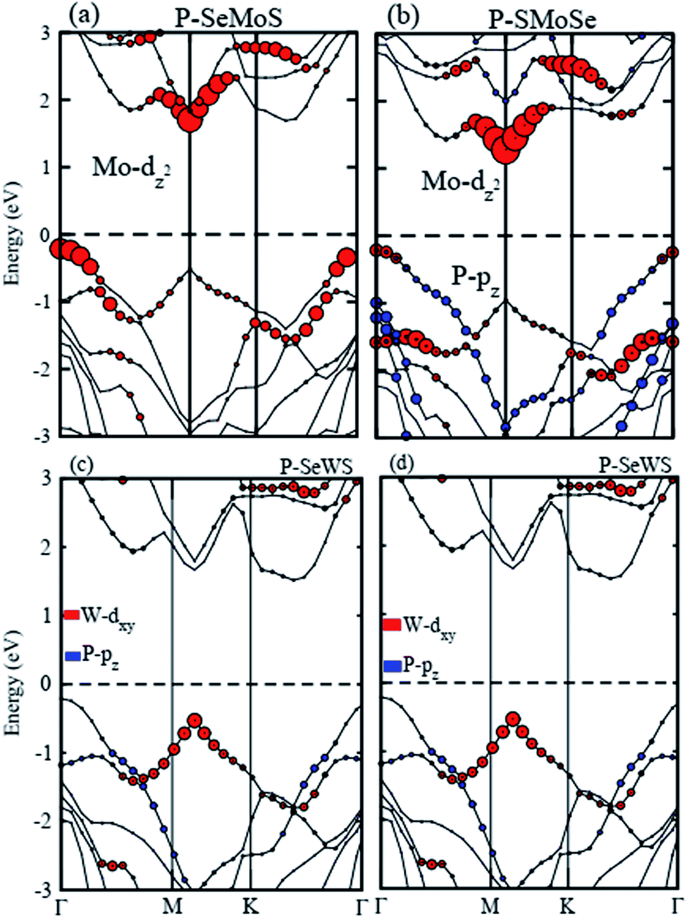 | ||
| Fig. 4 Weighted band structures of P–Mo(W)SSe vdW heterostructures. | ||
The charge density difference (Δρ) provides information about charge transfer across the interface and may be given as: Δρ = ρheterostructure − ρblueP − ρSMSe,SeMS where ρheterostructure, ρblueP, and ρSMSe,SeMS represent the charge density of the heterostructure, blueP and SMSe and SeMS monolayers, respectively. It is evident from Fig. 5(e and f) that charges are depleted from blueP and accumulated on SMoSe, SWSe (gain and loss of electrons is shown by cyan and yellow colors in Fig. 5), whereas the charge distribution is mainly present in the interfacial locality between blueP and nearby Se/S atoms, because of the difference between their electronegativities. To discuss charge redistribution in detail, the planar averaged charge density has been calculated along the z-direction perpendicular to the heterostructures as shown in Fig. 5(a–d). The values above zero (positive) in the figure indicate that the blueP gives electrons to SMSe, completing p-type doping in blueP and n-type doping in SMSe. Further, the Bader charge analysis technique50 is used for in depth concepts of the charge transfer mechanism from blueP to SMoSe, SWSe. It is noted that 0.32e(0.54e) and 0.21e(0.26e) fraction of charge has been transferred from blueP to SeMoS(SMoSe) and SeWS, SWSe monolayers. These indicated values show that in the calculated heterobilayer system, the blueP layer is an electron donor and SMoSe and SWSe layers are electron acceptors. This leads to a p(n)-type doping process in blueP(SMoSe and SWSe) in the studied heterobilayers. Furthermore, the transfer of charge between phosphorene and S/Se enhances an inner electric field partially detaches the photogenerated electrons in different atoms. This clearly shows a weak interaction between blueP and the SMSe monolayers; this characteristic has also been shown by GeC–Janus-TMDCs and ZnO–Janus-TMDCs.34,35
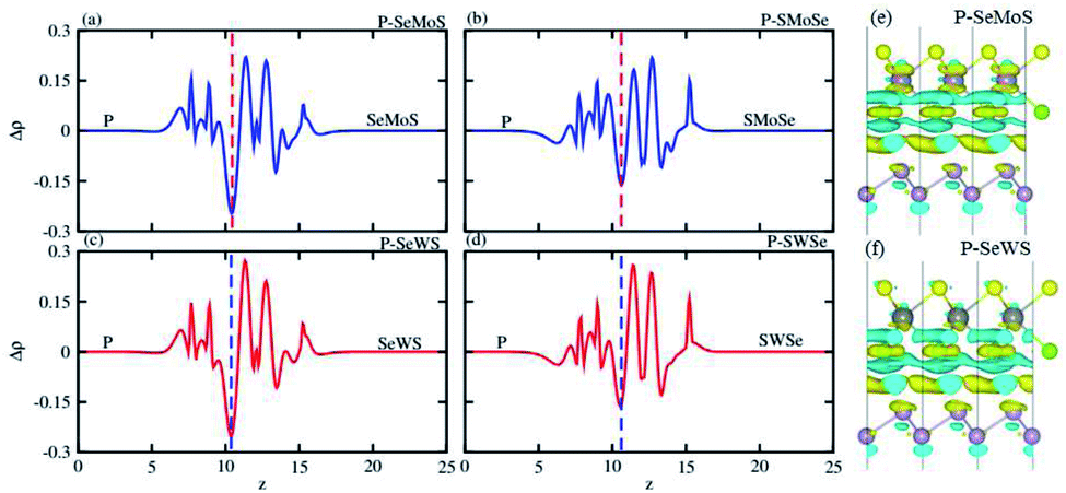 | ||
| Fig. 5 Planar-averaged charge density (a–d) and charge density difference (e and f) of PMo(W)SSe vdW heterostructures. | ||
The production of hydrogen gas under solar irradiation using a photocatalyst is in high demand for safe and environment friendly renewable energy sources. In general, the oxidation and reduction reaction for photocatalytic water splitting can be written as:  and
and  .51 The photocatalysis of water splitting consists of transportation and separation of photogenerated charge carrier electrons from the material to H+/H2 and holes to oxygen molecules. It has been reported that materials with a band gap value greater than 1.23 eV are suitable for photocatalytic water splitting. These outcomes lead to the result that active O2 and H2 transformation are achievable under the influence of visible light, which leads to a reasonable photocatalytic mechanism.52 The positions of the band edges of the studied heterostructures as compared with the standard reduction (−4.44 eV) and oxidation (−5.67 eV) potentials for water splitting at pH = 0 are obtained using HSE06, see Fig. 6. It is evident from our previous work that both the VB and CB edges of blue-P, MoSSe and WSSe Janus monolayers can be seen to be more positive and more negative than the redox potential of O2/H2O and H+/H2 respectively, which is very near to the previous studies.18,29,34,53 This recommends the idea that water oxidation and reduction can be feasible thermodynamically for the possible heterostructures. Furthermore, the energy levels of the VB and CB for P–Mo(W)SSe heterobilayers are much larger than the general redox potential, which provides enough energy to drag the photogenerated charge carrier electrons and respective holes to dissociate water molecules into O2/H2O and H+/H2, this phenomenon rates this material as a good water splitting photocatalyst. A similar trend has also been demonstrated in GeC–Janus-TMDCs and ZnO–Janus-TMDCs heterobilayers.34,35 In contrast, P–SMoSe is not capable to perform the reduction reaction and is suitable for the oxidation reaction, as displayed in Fig. 6. Thus, we suggest that P–SMoSe, blueP–SWSe heterobilayers are exciting materials for water splitting and suitable for the commercial scale production of solar hydrogen.
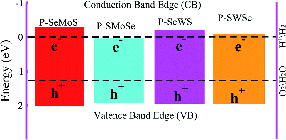 | ||
| Fig. 6 Valence and conduction band edges of both models of P–Mo(W)SSe vdW heterostructures with black dashed-lines representing the standard reduction (−4.44 eV) and oxidation (−5.67 eV) potentials for water dissociation into H+/H2 and O2/H2O, respectively. | ||
4 Conclusion
In summary, we have calculated the structural, electronic and photocatalytic behaviors of vdW heterostructures of blueP and Janus SMSe and SeMS (M = Mo, W) using first principles calculations. Our results show that blueP heterostructures with SMoSe and SWSe through an alternate order of chalcogenides at opposite sides in SMSe and SeMS are energetically and thermally stable. All stackings (except P–SeMoS) show type-II band alignment which enables the charge carrier mechanism and are ideal for solar panels. Interestingly, the VB and CB edge positions of both models of the studied heterobilayer systems straddle the standard redox potentials and are useful for dissociation of water into O2/H2O and H+/H2. However, P–SMoSe is only suitable for performing the oxidation reaction. These theoretical findings provide a way for useful designing of optoelectronic and future renewable energy devices.Conflicts of interest
The authors declare that there are no conflicts of interest regarding the publication of this paper.References
- N. Mounet, M. Gibertini, P. Schwaller, D. Campi, A. Merkys, A. Marrazzo, T. Sohier, I. E. Castelli, A. Cepellotti, G. Pizzi and N. Marzari, Two-dimensional materials from high-throughput computational exfoliation of experimentally known compounds, Nat. Nanotechnol., 2018, 13, 246–252 CrossRef CAS.
- A.-H. C. Neto and K. Novoselov, New directions in science and technology: two dimensional crystals, Rep. Prog. Phys., 2011, 74, 082501 CrossRef.
- X. Li and H. Zhu, Two-dimensional MoS2: Properties, preparation, and applications, J. Materiomics, 2015, 1(1), 33–44 CrossRef.
- A. Kuc, N. Zibouche and T. Heine, Influence of quantum confinement on the electronic structure of the transition metal sulfide TS2, Phys. Rev. B: Condens. Matter Mater. Phys., 2011, 83(24), 245213 CrossRef.
- K. Watanabe, T. Taniguchi and H. Kanda, Direct-bandgap properties and evidence for ultraviolet lasing of hexagonal boron nitride single crystal, Nat. Mater., 2004, 3, 404 CrossRef CAS.
- Y. Shi, C. Hamsen, X. Jia, K. K. Kim, A. Reina, M. Hofmann, A. L. Hsu, K. Zhang, H. Li, Z. Y. H. Juang and M. S. Dresselhaus, Synthesis of few-layer hexagonal boron nitride thin film by chemical vapor deposition, Nano Lett., 2010, 10, 4134–4139 CrossRef CAS.
- H. Liu, A. T. Neal, Z. Zhu, Z. Luo, X. Xu, D. Tománek and P. D. Ye, Phosphorene: an unexplored 2D semiconductor with a high hole mobility, ACS Nano, 2014, 8, 4033–4041 CrossRef CAS.
- L. Li, Y. Yu, G. J. Ye, Q. Ge, X. Ou, H. Wu, D. Feng, X. H. Chen and Y. Zhang, Black phosphorus field-effect transistors, Nat. Nanotechnol., 2014, 9, 372 CrossRef CAS.
- P. Eklund, M. Beckers, U. Jansson, H. Högberg and L. Hultman, The Mn+1AXn phases: materials science and thin-film processing, Thin Solid Films, 2010, 518, 1851 CrossRef CAS.
- N. I. Medvedeva, A. N. Enyashin and A. L. Ivanovskii, Modeling of the electronic structure, chemical bonding, and properties of ternary silicon carbide Ti3SiC2, J. Struct. Chem., 2011, 52, 785 CrossRef CAS.
- D. Voiry, J. Yang and M. Chhowalla, Recent strategies for improving the catalytic activity of 2D TMD nanosheets toward the hydrogen evolution reaction, Adv. Mater., 2016, 28, 6197–6206 CrossRef CAS.
- Y. Chen, H. Q. Sun and W. C. Peng, 2D transition metal dichalcogenides and graphene-based ternary composites for photocatalytic hydrogen evolution and pollutants degradation, Nanomaterials, 2017, 7, 62 CrossRef.
- J. Kim, A. Paul, P. A. Crowell, S. J. Koester, S. S. Sapatnekar, J. P. Wang and C. H. Kim, Spin-Based Computing: Device Concepts, Current Status, and a Case Study on a High-Performance Microprocessor, Proc. IEEE, 2014, 103, 106–130 Search PubMed.
- J. Zhang, S. Jia, I. Kholmanov, L. Dong, D. Er, W. Chen, H. Guo, Z. Jin, V. B. Shenoy, L. Shi and J. Lou, Janus Monolayer Transition-Metal Dichalcogenides, ACS Nano, 2017, 11(8), 8192–8198 CrossRef CAS.
- L. Dong, J. Lou and V. B. Shenoy, Large In-Plane and Vertical Piezoelectricity in Janus Transition Metal Dichalchogenides, ACS Nano, 2017, 11(8), 8242–8248 CrossRef CAS.
- C. Shang, B. Xu, X. Lei, S. Yu, D. Chen, M. Wu, B. Sun, G. Liu and C. Ouyang, Bandgap tuning inMoSSe bilayers: synergistic effects of dipole moment and interlayer distance, Phys. Chem. Chem. Phys., 2018, 20, 20919–20926 RSC.
- W. J. Yin, B. Wen, G. Z. Nie, X. L. Wei and L. M. Liu, Tunable dipole and carrier mobility for a few layer Janus MoSSe structure, J. Mater. Chem. C, 2018, 6, 1693–1700 RSC.
- X. Ma, X. Wu, H. Wang and Y. Wang, A Janus MoSSe monolayer: a potential wide solar-spectrum water-splitting photocatalyst with a low carrier recombination rate, J. Mater. Chem. A, 2018, 6, 2295–2301 RSC.
- Z. Zhu and D. Tomanek, Semiconducting layered blue phosphorus: a computational study, Phys. Rev. Lett., 2014, 112, 176802 CrossRef.
- C. Chowdhury and A. Datta, Exotic physics and chemistry of two-dimensional phosphorus: phosphorene, J. Phys. Chem. Lett., 2017, 8(13), 2909–2916 CrossRef CAS.
- T. K. Mukhopadhyay and A. Datta, Ordering and dynamics for the formation of two-dimensional molecular crystals on black phosphorene, J. Phys. Chem. C, 2017, 121(18), 10210–10223 CrossRef CAS.
- C. Chowdhury, S. Karmakar and A. Datta, Capping black phosphorene by h-BN enhances performances in anodes for Li and Na ion batteries, ACS Energy Lett., 2016, 1(1), 253–259 CrossRef CAS.
- J. L. Zhang, S. Zhao, C. Han, Z. Wang, S. Zhong, S. Sun, R. Guo, X. Zhou, C. D. Gu, K. D. Yuan, Z. Li and W. Chen, Epitaxial growth of single layer blue phosphorus: A new phase of two-dimensional phosphorus, Nano Lett., 2016, 16, 4903–4908 CrossRef CAS.
- J. Xiao, M. Long, X. Zhang, J. Ouyang, H. Xu and Y. Gao, Theoretical predictions on the electronic structure and charge carrier mobility in 2D Phosphorus sheets, Sci. Rep., 2015, 5, 9961 CrossRef CAS.
- C. Chowdhury, S. Jahiruddin and A. Datta, Pseudo-Jahn-Teller distortion in two-dimensional phosphorus: Origin of black and blue phases of phosphorene and band gap modulation by molecular charge transfer, J. Phys. Chem. Lett., 2016, 7(7), 1288–1297 CrossRef CAS.
- Q. F. Li, C. G. Duan, X. G. Wan and J. L. Kuo, Theoretical prediction of anode materials in Li-ion batteries on layered black and blue phosphorus, J. Phys. Chem. C, 2015, 119(16), 8662–8670 CrossRef CAS.
- L. Huang and J. Li, Tunable electronic structure of black phosphorus/blue phosphorus van der Waals p–n heterostructure, Appl. Phys. Lett., 2016, 108, 083101 CrossRef.
- J. F. Xie, M. S. Si, D. Z. Yang, Y. Zhang and D. S. Xue, A Theoretical Study of Blue Phosphorene Nanoribbons Based on First-Principles Calculations, J. Appl. Phys., 2014, 116, 073704 CrossRef CAS.
- W. Zhou, J. Chen, Z. Yang, J. Liu and F. Ouyang, Geometry and electronic structure of monolayer, bilayer, and multilayer Janus WSSe, Phys. Rev. B, 2019, 99, 075160 CrossRef.
- X. Gao, Y. Shen, Y. Ma, S. Wu and Z. Zhou, A water splitting photocatalysis: Blue phosphorus/g-GeC van der Waals heterostructure, Appl. Phys. Lett., 2019, 114, 093902 CrossRef.
- H. U. Din, M. Idrees, T. A. Alrebdi, C. V. Nguyen and B. Amin, Electric field tunable electronic properties of P-ZnO and SiC-ZnO van der Waals heterostructures, Comput. Mater. Sci., 2019, 164, 166 CrossRef CAS.
- B. J. Wang, X. H. Li, R. Zhao, X. L. Cai, W. Y. Yu, W. B. Li, Z. S. Liu, L. W. Zhang and S. H. Ke, Electronic structures and enhanced photocatalytic properties of blue phosphorene/BSe van der Waals heterostructures, J. Mater. Chem. A, 2018, 6(19), 8923–8929 RSC.
- F. Li, W. Wei, P. Zhao, B. Huang and Y. Dai, Electronic and optical properties of pristine and vertical and lateral heterostructures of Janus MoSSe and WSSe, J. Phys. Chem. Lett., 2017, 8, 5959–5965 CrossRef CAS.
- H. U. Din, M. Idrees, A. Albar, M. Shafiq, I. Ahmad, C. V. Nguyen and B. Amin, Rashba spin splitting and photocatalytic properties of GeC-M SSe (M= Mo, W) van der Waals heterostructures, Phys. Rev. B, 2019, 100(16), 165425 CrossRef CAS.
- M. Idrees, H. U. Din, S. U Reman, M. Shafiq, Y. Saeed, B. Dinh, C. Nguyen and B. Amin, Electronic properties and enhanced photocatalytic performance of van der Waals Heterostructures of ZnO and Janus transition metal dichalcogenides, Phys. Chem. Chem. Phys., 2020, 22, 10351–10359 RSC.
- P. E. Blöchl, Projector augmented-wave method, Phys. Rev. B: Condens. Matter Mater. Phys., 1994, 50, 17953–17979 CrossRef.
- G. Kresse and J. Hafner, VASP (Vienna, ab initio simulation package) software, Phys. Rev. B: Condens. Matter Mater. Phys., 1993, 47, 558–561 CrossRef CAS.
- G. Kresse, Effect of Er doping on the electronic structure optical properties of ZnO, Phys. Rev. B: Condens. Matter Mater. Phys., 1996, 54, 11169–11186 CrossRef CAS.
- S. Grimme, Semiempirical GGA-type density functional constructed with a long-range dispersion correction, J. Comput. Chem., 2006, 27, 1787 CrossRef CAS.
- J. P. Perdew, K. Burke and M. Ernzerhof, Generalized gradient approximation made simple, Phys. Rev. Lett., 1996, 77(18), 3865 CrossRef CAS.
- J. Heyd, G. E. Scuseria and M. Ernzerhof, Hybrid functionals based on a screened Coulomb potential, J. Chem. Phys., 2003, 118, 8207 CrossRef CAS.
- T. Teshome and A. Datta, Two-Dimensional Graphene-Gold Interfaces Serve as Robust Templates for Dielectric Capacitors, ACS Appl. Mater. Interfaces, 2017, 9(39), 34213–34220 CrossRef CAS.
- Y. G. Li, Y. L. Li, B. S. Sa and R. Ahujad, Catal. Sci. Technol., 2017, 7, 545 RSC.
- X. H. Li, B. J. Wang, X. L. Cai, W. Y. Yu, L. W. Zhang, G. D. Wang and S. H. Ke, RSC Adv., 2017, 7, 44394 RSC.
- J. M. Liao, B. S. Sa, J. Zhou, R. Ahuja and Z. M. Sun, J. Phys. Chem. C, 2014, 118, 17594 CrossRef CAS.
- H. U. Din, M. Idrees, G. Rehman, C. V. Nguyen, L.-Y. Gan, I. Ahmad, M. Maqbool and B. Amin, Electronic structure, optical and photocatalytic performance of SiC-MX2 (M = Mo, W and X = S, Se) van der Waals heterostructures, Phys. Chem. Chem. Phys., 2018, 20, 24168 RSC.
- H. P. Komsa and A. V. Krasheninnikov, Electronic structures and optical properties of realistic transition metal dichalcogenide heterostructures from first principles, Phys. Rev. B: Condens. Matter Mater. Phys., 2013, 88, 085318 CrossRef.
- S. Nakamura, M. Senoh, N. Iwasa and S.-i. Nagahama, High-brightness InGaN blue, green and yellow light-emitting diodes with quantum well structures, Jpn. J. Appl. Phys., 1995, 34, L797 CrossRef CAS.
- Y. Arakawa and A. Yariv, Quantum well lasers–Gain, spectra, dynamics, IEEE J. Quantum Electron., 1986, 22, 1887–1899 CrossRef.
- G. Henkelman, A. Arnaldsson and H. Jónsson, A fast and robust algorithm for Bader decomposition of charge density, Comput. Mater. Sci., 2006, 36(3), 354 CrossRef.
- K. Ren, C. Ren, Y. Luo, Y. Xu, J. Yu, W. Tang and M. Sun, Using van der Waals heterostructures based on two-dimensional blue phosphorus and XC (X= Ge, Si) for water-splitting photocatalysis: a first-principles study, Phys. Chem. Chem. Phys., 2019, 21, 9949–9956 RSC.
- W. Mtangi, F. Tassinari, K. Vankayala, A. Vargas Jentzsch, B. Adelizzi, A. R. Palmans, C. Fontanesi, E. Meijer and R. Naaman, Control of electrons’ spin eliminates hydrogen peroxide formation during water splitting, J. Am. Chem. Soc., 2017, 139(7), 2794–2798 CrossRef CAS.
- M. Idrees, H. U. Din, S. A. Khan, I. Ahmad, L. Y. Gan, C. V. Nguyen and B. Amin, Van der Waals heterostructures of P, BSe, and SiC monolayers, J. Appl. Phys., 2019, 125(9), 094301 CrossRef.
| This journal is © The Royal Society of Chemistry 2020 |