
 Open Access Article
 This Open Access Article is licensed under a Creative Commons Attribution-Non Commercial 3.0 Unported Licence
Mechanism for hydrogen evolution from water splitting based on a MoS2/WSe2 heterojunction photocatalyst: a first-principle study
Yazhou Wang ab,
Tong Liuab,
Weizhi Tianab,
Ying Zhangab,
Pengyue Shanab,
Yunjian Chenab,
Wanhang Weiab,
Hongkuan Yuanc and
Hong Cui*ab
ab,
Tong Liuab,
Weizhi Tianab,
Ying Zhangab,
Pengyue Shanab,
Yunjian Chenab,
Wanhang Weiab,
Hongkuan Yuanc and
Hong Cui*ab
aSchool of Mechanical Engineering, Shaanxi University of Technology, Hanzhong, Shaanxi 723001, China. E-mail: hongcui@snut.edu.cn
bShaanxi Key Laboratory of Industrial Automation, Shaanxi University of Technology, Hanzhong, Shaanxi 723001, China
cSchool of Physical Science and Technology, Southwest University, Chongqing, 400715, P. R. China
First published on 11th November 2020
Abstract
In this study, density functional theory and hybrid functional theory are used to calculate the work function and energy band structure of MoS2 and WSe2, as well as the binding energy, work function, energy band structure, density of states, charge density difference, energy band alignment, Bader charge, and H adsorption free energy of MoS2/WSe2. The difference in work function led to the formation of a built-in electric field from WSe2 to MoS2, and the energy band alignment indicated that the redox reactions were located on the MoS2 and WSe2 semiconductors, respectively. The binding energy of MoS2 and WSe2 indicated that the thermodynamic properties of the heterogeneous structure were stable. MoS2 and WSe2 gathered electrons and holes, respectively, and redistributed them under the action of the built-in electric field. The photogenerated electrons and holes were enriched on the surface of WSe2 and MoS2, which greatly improved the efficiency of hydrogen production by photocatalytic water splitting.
Introduction
To further develop high-energy green hydrogen, the production of hydrogen using photocatalytic water splitting (WS) has attracted significant interest from both academia and industry.1 During light irradiation, electrons in photocatalyst valence bands (VB) absorb photon energy and then become excited from the VB to the conduction bands (CB). This enables them to participate in the hydrogen evolution reaction (HER). The holes left in the VB can then participate in the oxygen evolution reaction (OER). This is another reaction for WS that is more difficult than the HER.2,3After Fujishima and Honda used the photocatalyst TiO2 for WS to successfully produce hydrogen in 1972,4 researchers became committed to developing better photocatalysts for producing hydrogen.5 Photocatalytic hydrogen generation by WS must meet two photocatalyst requirements under light conditions. The first requirement is that the energy to excite electrons from the VB of the photocatalytic to their CB must be greater than the WS voltage and the semiconductor bandgap. The second requirement is the CB potential in the energy band needs to be more negative than the hydrogen reduction potential, and the VB potential must be more positive than the oxidation potential.5–7 According to the equation λ = 1240/Eg (λ (nm), Eg represent the optical wavelength and semiconductor band gap), appropriately reducing the semiconductor band gap in excess of that required for WS (theoretically 1.23 eV) can reduce the requirements for the energy that the electron absorbs from light, broaden the light absorption range, and improve the efficiency of hydrogen evolution.8
Since the method of exfoliating graphene was discovered,9 two-dimensional (2D) materials research has been developing rapidly, including transition metal dichalcogenides (TMD), especially for the monolayer TMD,10 which has excellent optoelectronic properties compared with bulk TMD, such as superconductivity and a semiconducting behavior.11,12 According to Voiry's research, TMDs, when used as photocatalysts, can broaden the range (≥420 nm) of light absorption of visible light, but its stability and activity is not satisfactory.13 The atomic-thickness monolayer MoS2, which features good low light detection,14 high photosensitivity, and high carrier mobility, has high light absorption efficiency and generates a large number of photogenerated electrons and hole pairs under light conditions that are crucial to HER and OER,15 respectively, giving it the potential to be a photocatalytic material. Hinnemann studied hydrogen release using MoS2 nanoparticles supported on graphite as a catalyst for water electrolysis, and he found that the binding free energy of atomic hydrogen to the catalyst was close to zero  .16 WSe2 is also considered to be one of the most promising optoelectronic device materials for the future.17 For example, the photocells based on WSe2 have high efficiency and thermal stability because of its high charge carrier mobility and mechanical flexibility.18–20 Kumar studied the synthesis of heterojunctions using WSe2 as the substrate and found that MoSe2/WSe2 showed decent new photoelectric characteristics (enhanced photoluminescence, smaller electron effective masses and high electron mobility).21 McKone investigated the solar energy conversion efficiency of WSe2 photocatalytic hydrogen production (67%) using Pt/Ru as a co-catalyst (60%).22 Meng-Yen Tsai et al. found that the Fermi energy levels moved towards VBM and CBM when WSe2 were P and N doped, respectively,23 which was favorable for changing the photocatalytic activity of WSe2.
Photocatalytic heterojunctions based on TMD synthesis have been preliminarily studied. For example, Charlie Tsai et al. studied hydrogen release with MoSe2/WSe2 heterojunctions based on the density function theory (DFT) because MoSe2 and WSe2 nanofilms and nanosheets have been shown to be active for electrochemical H2 evolution. They found that enhanced activity was located at the edges of MoSe2 and WSe2.24 Wang et al. studied the photocatalytic performance of the direct Z-scheme MoSe2/SnS2 van der Waals heterojunction. They found that the light absorption wavelength was widened to 600 nm, but the oxidation potential could be further increased to produce hydrogen more efficiently.25 Ho et al. deposited MoS2 on CdS to form a CdS/MoS2 heterojunction and used it as a photoanode to study its photocatalytic activity. They found that heterojunction formation contributed to increased carrier concentration and conductivity.26 Hellstern et al. studied solar energy conversion efficiency using MoS2/TiO2/CdS/CGSe as a photocathode, and they found that the catalyst produced H2S during the preparation process.27 Efficiency needs to be improved further to meet the demand for energy.
According to Jiang's study, any MX2 (M = molybdenum (Mo) and tungsten (W); X = sulphur (S) and selenium (Se)) material cannot be used directly as a full spectrum photocatalyst because its valence band maximum (VBM) and conduction band minimum (CBM) energies do not match the oxidation reduction potential of HER and OER.28 Monolayer MoS2 photogenerated electrons and holes have high mobility, which is favorable for photocatalytic hydrogen production.29–32 In this study, a new design of a photocatalytic van der Waals heterojunction MoS2/WSe2 is proposed using TMDs with physical and optoelectronic properties as substrates. In addition, HER and OER generation are studied to enhance the photocatalytic activity with higher redox activity.23,33
Methodology
In this paper, we performed the initial calculations using first principles based on DFT and performed the single point calculations with a hybrid functional theory (HSE (06)). We carried out both calculations using the Vienna ab initio simulation package (VASP).34 The exchange correlation function used the Perdew–Burke–Ernzerh (PBE) function of the generalized gradient approximation (GGA). We set the plane wave cutoff energy at 500 eV.34–39 The effective band structure (EBS) proposed by Zunger et al. could transform the band structure of a supercell into the Brillouin region of a primitive cell, which provided favorable conditions for the correct analysis of the supercell energy band. Therefore, we calculated the effective band structure of the supercell by the energy band unfolding method.40–42 The structure relaxation energy convergence criterion was 1 × 10⁻⁶ eV. The force convergence criterion was −2 × 10⁻² eV Å−2. The Brillouin region was divided into 6 × 6 × 1 and 4 × 4 × 1 for the hexagonal crystalline MoS2 and WSe2 and MoS2/WSe2, respectively. The Brillouin regions are shown in Fig. 2(b) and (d), and the calculated path is Γ → M → K → Γ.43,44 We set the large vacuum space of 20 Å along the perpendicular direction to the 2D plane to minimize the interactions between the adjacent heterostructures. When performing first principles calculations, we introduced HSE (06) to accurately characterize the correct energy band structure and electronic properties of the material. The study used the mixing parameter, α = 0.25, for accurate hybrid generalization calculations, because the HSE (06) hybrid generalization results provided more accurate calculations, including those for band structure, density of states (DOS), electronic properties, and work function, compared with PBE functional.45,46 Therefore, the research in this article is based on the results of HSE (06) hybrid functional calculations.Results and discussion
TMD exists in several structural phases produced by the coordination of transition metal atoms and different VIA atoms. This study adopted the ABA-stacked trigonal (2H) structure of common structural features. As shown in Fig. 1, the monolayer TMD can be viewed as a sandwich structure consisting of two layers of VIA atoms (A and A′) embedded with one layer of transition metal elements (B and B′).21,47 | ||
| Fig. 1 2(H) MoS2 (a) and 2(H) WSe2 (b) structures: green (A) spheres, indigo (B) spheres, cyan (A′) spheres and pink (B′) spheres represent S atoms, Mo atoms, Se atoms and W atoms, respectively. | ||
We constructed and optimized the monolayer MoS2 and monolayer WSe2 models. The bond lengths of Mo–S and W–Se were 2.412 Å and 2.542 Å, respectively, as shown in Fig. 2(a). Then, we constructed the heterostructure with MoS2 and WSe2 model structure particles. After full relaxation as shown in Fig. 2(c), the bond lengths of Mo–S and W–Se were 2.412 Å and 2.542 Å, respectively. As shown in Fig. 2(c), both the semiconductors layer distance was d = 3.70 Å, indicating the heterojunction was a van der Waals heterojunction.48,49 The van der Waals effect enabled the tight bonding of different 2D nanomaterials (MoS2 and WSe2), and the van der Waals heterojunctions with ultrafast carrier migration accelerated the charge migration.50 As shown in Fig. 2(a), the lattice volumes of MoS2, WSe2, and MoS2/WSe2 were 325.63 Å3, 346.30 Å3, and 334.22 Å3, respectively, and EMoS2/WSe2, EMoS2, and EWSe2 were −173.75 eV, −86.987 eV, and −86.485 eV in the constructed MoS2/WSe2 heterojunction. The thermodynamic stability of the heterojunction can be achieved with eqn (1):51
| Eb = EMoS2/WSe2 − EWSe2 − EMoS2 | (1) |
 | ||
| Fig. 2 (a) Spatial structure of the hexagonal crystal MoS2 and WSe2: blue and wine spheres represent S, Se atoms and Mo, W atoms; (c) MoS2/WSe2 stacked structure of MoS2 and WSe2: green, indigo, cyan, and pink spheres represent S atoms, Mo atoms, Se atoms, and W atoms, respectively; (b) Brillion region high symmetry point path schematic three-dimensional view; and (d) top view. | ||
Here, negative binding energy (−0.287 eV) indicated the MoS2/WSe2 heterojunction had stable thermodynamic properties.
The complex process of hydrogen production by photocatalytic WS included the generation, transformation, recombination, and surface reactions of photogenerated electron and hole pairs. We plotted and used the electrostatic potential function diagrams of MoS2, WSe2, and MoS2/WSe2 heterojunctions to study the photocatalyst carrier transfer and analyze the photocatalytic efficiency, as shown in Fig. 3(a)–(c), respectively. We obtained the work function Φ with eqn (2).51–54 To further investigate the charge distribution of in the heterojunctions, we plotted the plane average charge density difference in Fig. 3(d) and the charge density difference in Fig. 3(e). The plane average charge density difference and charge density difference Δρ were obtained by eqn (3) and (4), respectively:55
| Φ = Eva − Ef | (2) |
 | (3) |
| Δρ = ρMoS2/WSe2 − ρMoS2 − ρWSe2 | (4) |
 | ||
| Fig. 3 Electrostatic potential of (a) MoS2, (b) WSe2, and (c) MoS2/WSe2; (d) plane average charge density difference; and (e) the charge density difference for MoS2/WSe2, where cyan and yellow represent charge accumulation and depletion, respectively. | ||
As shown in Table 1, the work functions of MoS2, WSe2, and MoS2/WSe2 are 5.25 eV, 4.36 eV, and 4.80 eV, respectively, which is consistent with the PBE functional.53 The work functions of MoS2, WSe2, and MoS2/WSe2 are 5.63 eV, 5.08 eV, and 5.22 eV, respectively under the HSE (06) hybrid functional condition. The Fermi energy level of MoS2 was lower than that of WSe2, and the electrons flowed spontaneously from WSe2 to MoS2 until the Fermi levels on both sides reached the same potential. Thus, the WSe2 side was positively charged, whereas the MoS2 side was negatively charged at the interface. Hence, energy band bending would occur and a built-in electric field would be formed at the junction of the MoS2 surface and WSe2 surface interface. The formation of a built-in electric field promoted the separation and transport of photogenerated electrons and holes, inhibited the recombination of photogenerated electrons and holes, and prolonged the life of photogenerated electrons and holes, better promoting photogenerated carrier transfers to the HER and OER sites of the MoS2/WSe2 heterojunction, and increasing photocatalytic reaction efficiency.
| Materials | Eva (eV) | Ef (eV) | Φ | |||
|---|---|---|---|---|---|---|
| PBE | HSE (06) | PBE | HSE (06) | PBE | HSE (06) | |
| MoS2 | 2.36 | 2.13 | −2.89 | −3.50 | 5.25 | 5.63 |
| WSe2 | 4.26 | 2.05 | −0.1 | −3.03 | 4.36 | 5.08 |
| MoS2/WSe2 | 4.19 | 4.20 | −0.61 | −0.83 | 4.80 | 5.22 |
Fig. 3(d) quantitatively depicts the plane averaged charge density difference along the lattice c direction. It is evident that the negative charge accumulated mainly on the MoS2, whereas positive charge accumulated on the WSe2. The amount of the charge accumulation and transformation was zero on both sides of the heterojunction, which verified that the thickness of the heterojunction vacuum layer was perfectly suitable to avoid errors in the analytical calculations because of an insufficient vacuum layer thickness. Fig. 3(e) depicts the redistribution of negative charge and positive charge in heterojunctions, with cyan representing the negative charge accumulation region and yellow representing the negative charge depletion region. The negative charge was concentrated mainly on the surface of MoS2 and around the Mo atoms, and a small amount of negative charge aggregation appeared inside WSe2 between W and Se atoms. Electron depletion occurred on the WSe2 semiconductor. The MoS2 semiconductor had a small amount of charge migration between the Mo and S atoms. Fig. 3(d) and (e) showed the redistribution of negative and positive charge on different semiconductors resulting from the built-in electric field directed from the WSe2 surface toward the MoS2 surface. The redistribution of charge was in agreement with the formation of a built-in electric field and the work function, which favored the photocatalytic reaction.56
Under illumination, the electrons on photocatalyst VB absorbed photon energy and then became excited from the VB to CB, and the photogenerated holes remained on the VB. For direct bandgap semiconductors, the electrons on the VB with energy greater than or equal to the bandgap jumped directly from the VB to the CB at the bandgap.57 To study the photocatalytic properties of the photocatalyst, we first calculated the energy bands of MoS2 and WSe2 by the PBE function to prepare the HSE (06) hybrid function calculations. The CBM and the VBM were displayed at the K point in the Brillouin region. The results, under the PBE functional, showed that the bandgap (1.68 eV) of the monolayer MoS2 was consistent with Manzeli's experimental results (1.71 eV), and the bandgap (1.60 eV) of the monolayer WSe2 was consistent with Lee's experimental results (1.66 eV).47,58,59 The energy band structures of MoS2, WSe2, and MoS2/WSe2 were further calculated by HSE (06) hybrid function. Thus, a more precise analysis of the efficiency of heterojunction photocatalytic hydrogen production is shown in Fig. 4. In Fig. 4(a), the CBM and VBM of monolayer MoS2 lie in the K point in the Brillouin region. So, the monolayer MoS2 was a direct bandgap, which was consistent with the conclusion that the direct bandgap Eg was 2.16 eV, and the previous calculations were in agreement with the experimental results of Manzeli (2.16 eV) and Hill (2.16 ± 0.04 eV).47,60 Fig. 4(b) shows the energy band structure of the monolayer WSe2, with both its CBM and VBM appearing at the K point (direct bandgap 2.08 eV), which was consistent with the experimental results of Zribi (2.08 eV), and Chiu (2.08 ± 0.1 eV).61,62 This result demonstrated that the calculation method was correct. Fig. 4(c) shows both the heterojunction CBM and VBM obtained at the K point, which can broaden the light absorption range. In addition, the CBM and VBM of MoS2 were contributed to primarily by Mo atoms. The CBM and VBM of WSe2 were contributed to primarily by W atoms with a small contribution from Se atoms, whereas the VB was contributed to primarily by Se atoms. The MoS2/WSe2 heterojunction CBM was contributed to primarily by the Mo atoms, and the VBM was contributed to primarily by W atoms.
 | ||
| Fig. 4 Energy band structure of (a) MoS2, (b) WSe2, and (c) the MoS2/WSe2 heterojunction. | ||
To quantitatively investigate the interface electronic structure and identification of the nature of the orbitals, we calculated the projected density of state (PDOS) of the MoS2, WSe2, and the MoS2/WSe2 heterostructure, and the total density of state (TDOS) of the MoS2/WSe2 heterostructure in Fig. 5. Fig. 5(a) indicates that the VBM and CBM of the MoS2 were occupied by the Mo(d) atomic orbitals of MoS2. Fig. 5(b) indicates that the VBM and CBM of the WSe2 were occupied by the W(d) atomic orbitals of WSe2. Fig. 5(c) indicates that the VBM of the MoS2/WSe2 heterostructure was occupied by the atomic orbitals of WSe2. The CBM of the MoS2/WSe2 heterostructure was occupied primarily by the atomic orbitals of MoS2, and the atomic orbitals of MoS2 were higher than those of WSe2. Fig. 5(d)–(f) show that the VBM and CBM of the MoS2/WSe2 heterostructure were occupied by the W atoms and Mo atoms, respectively. Fig. 5(e) and (f) further show that the W(s) and W(p) orbital contributions of WSe2 were smaller than those of W(d) orbits, and the Mo(s) and Mo(p) orbital contributions of MoS2, which were significantly smaller than those of the Mo(d) orbits. Most importantly, this analysis of DOS was in agreement with the results of the band structure, as shown in Fig. 4(a)–(c).
 | ||
| Fig. 5 PDOS of (a) MoS2, (b) WSe2, and (c) TDOS and PDOS of the MoS2/WSe2 heterostructure; (d) PDOS of the heterostructure; (e) PDOS of the W elements on the VB of heterostructure; and (f) PDOS of the Mo elements on the CB of heterostructure. | ||
Combining the analysis of the work function and the Fermi level in Fig. 3, we studied the mechanism of hydrogen production by photocatalytic WS of MoS2/WSe2. As shown on the left side of Fig. 6(a), the Fermi level of MoS2 was lower than that of WSe2. An electrostatic potential difference formed because of the difference between Fermi levels when MoS2 and WSe2 were in contact, and the electrons flowed spontaneously from the high Fermi level to the low Fermi level under the drive of the potential difference until the Fermi levels reach equilibrium. Hence, the positive charge and negative charge accumulated mainly on the WSe2 side and MoS2 sides at the interface, respectively. Then a built-in electric field from WSe2 to MoS2 formed at the junction of the MoS2 surface and WSe2 surface interface, and the VB of WSe2 and CB of MoS2 occurred by bending upward and downward, respectively, as shown in Fig. 6(a) (right). The photocatalytic reaction mechanism and transfer of photogenerated electrons and holes of the MoS2/WSe2 heterostructure are illustrated in Fig. 6(b). Under illumination, electrons absorbed photon energy and then became excited from the VB of MoS2 and WSe2 to their CB; simultaneously, photoexcited holes were left in their VB. The built-in electric field from WSe2 surface to MoS2 surface accelerated the transfer of photoexcited electrons from the CB of MoS2 to the VB of WSe2, and resulted in the recombination of electrons and holes in the VB of WSe2. Simultaneously, the built-in electric field also restrained the photoexcited electrons in the CB of WSe2 to flow into the CB of MoS2 and photoexcited holes in the VB of MoS2 to transfer to the VB of WSe2. Therefore, under the built-in electric field driving, photoexcited electrons in the CB of MoS2 and holes in the VB of WSe2 were consumed. Conversely, the photoexcited electrons and holes naturally accumulated in the CB of WSe2 and VB of MoS2, respectively. The separation of photoexcited electrons and holes in space prolonged their lifetime and increased the probability of the photoexcited electrons and holes participating in the HER and OER on the surface, respectively, which effectively improved the photocatalytic activity of the MoS2/WSe2 heterostructure. This analysis indicated that MoS2/WSe2 heterostructure was a direct Z-scheme photocatalyst.2,63 As shown in Fig. 6(b), the photoexcited electrons of direct Z-scheme MoS2/WSe2 heterostructure accumulated in the CB of WSe2, and the CB edge potential of WSe2 was −0.421 eV (vs. NHE), which was more negative than that of H+/H2 (0 eV), and had enough ability to reduce H+ to H2. Additionally, the photoexcited holes accumulated at the VB of MoS2, and the corresponding VB edge potential of MoS2 was 2.256 eV, which was more positive than that of O2/H2O (1.23 eV) and had sufficient ability to produce O2. Therefore, the direct Z-scheme MoS2/WSe2 heterostructure exhibited better photocatalytic performance than either MoS2 or WSe2 alone.
 | ||
| Fig. 6 (a) Z-scheme semiconductor staggered energy band principles, untouched (left), touched (right); and (b) MoS2 and WSe2 band alignment. The pink solid line in the figure corresponds to the CBM in Fig. 4(a) and (b), the blue solid line corresponds to the VBM in Fig. 4(a) and (b); the red dotted line, green dotted line, pink dotted line, and blue dotted line represent the Fermi level, the vacuum level, the minimum reduction potential of hydrogen generated by WS, and the minimum oxidation potential of the water oxidation reaction, respectively. | ||
The charge transfer of the photocatalyst determined the hydrogen production efficiency of the photocatalyst, and we calculated the Bader charge to study the charge transformation in the catalyst.64,65
As shown in Fig. 7, we calculated the Bader charge of MoS2, WSe2, and MoS2/WSe2 heterostructure and plotted Tables 2 and 3 based on the number of charges carried by each atom. Mo and S atoms are more charged than W and Se atoms, respectively. Transition metal atoms are twice as charged as S-group atoms.
 | ||
| Fig. 7 Atomic number of semiconductor materials: (a) MoS2, (b) WSe2, and (c) MoS2/WSe2 heterostructure. | ||
| Elements | Charge (e) | Elements | Charge (e) |
|---|---|---|---|
| S1 | −0.95046 | W1 | 0.96352 |
| S2 | −0.95027 | W2 | 0.96713 |
| S3 | −0.95041 | W3 | 0.96713 |
| S4 | −0.95024 | W4 | 0.97074 |
| S5 | −0.93441 | Se1 | −0.45907 |
| S6 | −0.93408 | Se2 | −0.45907 |
| S7 | −0.93441 | Se3 | −0.45907 |
| S8 | −0.93401 | Se4 | −0.45907 |
| Mo1 | 1.88457 | Se5 | −0.50806 |
| Mo2 | 1.88457 | Se6 | −0.50806 |
| Mo3 | 1.88457 | Se7 | −0.50806 |
| Mo4 | 1.88457 | Se8 | −0.50806 |
| Elements | Charge (e) | Elements | Charge (e) |
|---|---|---|---|
| S1 | −0.58967 | W1 | 0.92161 |
| S2 | −0.58968 | W2 | 0.92161 |
| S3 | −0.58953 | W3 | 0.92163 |
| S4 | −0.58969 | W4 | 0.92138 |
| S5 | −0.58667 | Se1 | −0.4471 |
| S6 | −0.58668 | Se2 | −0.44709 |
| S7 | −0.58668 | Se3 | −0.44712 |
| S8 | −0.58669 | Se4 | −0.44712 |
| Mo1 | 1.17307 | Se5 | −0.47121 |
| Mo2 | 1.17307 | Se6 | −0.47121 |
| Mo3 | 1.17306 | Se7 | −0.47098 |
| Mo4 | 1.17293 | Se8 | −0.47124 |
Combining Tables 2 and 3, it is found that the charge of all elements in the heterojunction decreases when MoS2 forms a heterojunction with WSe2, especially the charge of Mo, S atoms decreases more than that of W, Se atoms, which indicates that part of the electrons of MoS2 move to WSe2, which is consistent with the results of the previous analysis, and indicates that the charge of MoS2 and WSe2 is partially free in the heterojunction as free electrons and does not participate in atomic bonding, which helps to improve the hydrogen production efficiency of the photocatalyst.
As shown in Fig. 8, to characterize the efficiency of photocatalytic WS for hydrogen production, we constructed a hydrogen adsorption model for the heterojunction and calculated the adsorption free energy for hydrogen at the different sites. The adsorption free energy data are shown in Table 4.
| EF = Eh–H2 − Eh − EH2 + 0.24 | (5) |
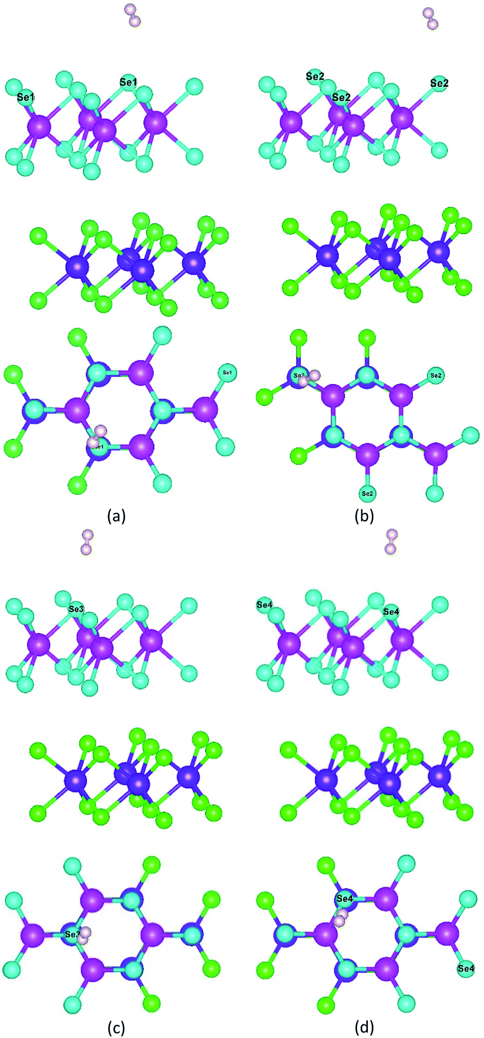 | ||
| Fig. 8 Hydrogen adsorption model for different adsorption sites: (a) Se1 site, (b) Se2 site, (c) Se3 site, and (d) Se4 site. | ||
| Sites | EH2 (eV) | Eh–H2 (eV) | EF (eV) |
|---|---|---|---|
| Se1 | −6.77 | −180.32 | 0.26 |
| Se2 | −6.76 | −180.32 | 0.25 |
| Se3 | −6.76 | −180.32 | 0.25 |
| Se4 | −6.76 | −180.32 | 0.25 |
As shown in Table 4, the free energies of Se1, Se2, Se3, and Se4 atoms for hydrogen were 0.26 eV, 0.25 eV, 0.25 eV, and 0.25 eV, respectively. They all were close to 0 eV, which indicated that the heterojunction did not have the adsorption effect on hydrogen after the generation of hydrogen, and the generated hydrogen could actively diffuse and failed to form hydrogen molecules clustered around the active site.67
Conclusions
In this study, we designed a MoS2/WSe2 van der Waals heterojunction to improve the efficiency of photocatalytic WS for hydrogen evolution. We performed all computations, including structure relaxation, energy band, DOS, electronic properties, and work function, based on DFT and HSE (06). Before performing the HSE (06) calculations, we used DFT based on the first principles for the initial calculations. We analyzed all results based on calculations of HSE (06) hybrid functional theory. The energy calculation results showed that the formation energy of the MoS2/WSe2 heterojunction was negative, so the thermodynamic properties of the heterojunction were stable. The work function calculations showed that the electrons flowed spontaneously from WSe2 to MoS2 until a potential equilibrium was reached on both semiconductors after the formation of the heterojunction, which resulted in an accumulation of a charge on one side of the heterojunction. Hence, a built-in electric field was established within the heterojunction that prevented the flow of photogenerated electrons from the CB of WSe2 to that of MoS2, stopped the flow of holes from the VB of MoS2 to WSe2, and facilitated the flow of photogenerated electrons from the MoS2 CB to recombine with the holes in the VB of WSe2. In this way, photogenerated electrons and holes accumulated in the CB of WSe2 and the VB of MoS2, respectively. This meant that reduction reactions proceeded at WSe2 and oxidation reactions proceeded at MoS2. The energy band calculations showed that the monolayer MoS2 and WSe2 both had direct bandgaps. When MoS2 and WSe2 were in contact, the CB potential of WSe2 was more negative than that of MoS2, and the VB potential of MoS2 was more positive than the VBM of WSe2. The orbital contributions of each element in MoS2, WSe2, and MoS2/WSe2 to VBM and CBM in combination with the DOS-assisted energy band structures were also analyzed. All of the results indicated that MoS2/WSe2 was a direct Z-scheme heterojunction. Photocatalytic HER and OER occurred on the CB of WSe2 and the VB of MoS2. Finally, we calculated the Bader charges of MoS2, WSe2, and MoS2/WSe2 and analyzed the charge transfer characterization active sites. We constructed the heterojunction hydrogen adsorption model to analyze the adsorption performance of heterojunction on hydrogen after hydrogen generation. All of the results showed that MoS2/WSe2, with great thermodynamic stability and strong redox ability, could be used as a WS catalyst for hydrogen production.Conflicts of interest
There are no conflicts to declare.Acknowledgements
This research was funded by the National Natural Science Foundation of China (No. 61701288, No. 51706128), the Key Scientific Research Project of the Shaanxi Provincial Education Department (No. 20JS019) and the Postgraduate Innovation Project of the Shaanxi University of Technology (No. SLGYCX2026).References
- L. Yang, X. Li, G. Zhang, P. Cui, X. Wang, X. Jiang, J. Zhao, Y. Luo and J. Jiang, Nat. Commun., 2017, 8, 16049 CrossRef CAS.
- Q. Xu, L. Zhang, J. Yu, S. Wageh, A. A. Al-Ghamdi and M. Jaroniec, Mater. Today, 2018, 21, 1042–1063 CrossRef CAS.
- M. Z. Rahman, M. G. Kibria and C. B. Mullins, Chem. Soc. Rev., 2020, 49, 1887–1931 RSC.
- A. Fujishima and K. Honda, Nature, 1972, 238, 37–38 CrossRef CAS.
- C. A. Rodriguez, M. A. Modestino, D. Psaltis and C. Moser, Energy Environ. Sci., 2014, 7, 3828–3835 RSC.
- H. Sun, C. Tian, G. Fan, J. Qi, Z. Liu, Z. Yan, F. Cheng, J. Chen, C.-P. Li and M. Du, Adv. Funct. Mater., 2020, 1910596 CrossRef CAS.
- Y.-J. Yuan, D. Chen, Z.-T. Yu and Z.-G. Zou, J. Mater. Chem. A, 2018, 6, 11606–11630 RSC.
- J. Yan, T. Wang, G. Wu, W. Dai, N. Guan, L. Li and J. Gong, Adv. Mater., 2015, 27, 1580–1586 CrossRef CAS.
- A. K. Geim and K. S. Novoselov, Nat. Mater., 2007, 6, 183–191 CrossRef CAS.
- R. Tenne, L. Margulis, M. Genut and G. Hodes, Nature, 1992, 360, 444–446 CrossRef CAS.
- X. Yu and K. Sivula, Chem. Mater., 2017, 29, 6863–6875 CrossRef CAS.
- D. Braga, I. Gutiérrez Lezama, H. Berger and A. F. Morpurgo, Nano Lett., 2012, 12, 5218–5223 CrossRef CAS.
- D. Voiry, J. Yang and M. Chhowalla, Adv. Mater., 2016, 28, 6197–6206 CrossRef CAS.
- D.-H. Kang, S. R. Pae, J. Shim, G. Yoo, J. Jeon, J. W. Leem, J. S. Yu, S. Lee, B. Shin and J.-H. Park, Adv. Mater., 2016, 28, 7799–7806 CrossRef CAS.
- O. Lopez-Sanchez, D. Lembke, M. Kayci, A. Radenovic and A. Kis, Nat. Nanotechnol., 2013, 8, 497–501 CrossRef CAS.
- B. Hinnemann, P. G. Moses, J. Bonde, K. P. Jørgensen, J. H. Nielsen, S. Horch, I. Chorkendorff and J. K. Nørskov, J. Am. Chem. Soc., 2005, 127, 5308–5309 CrossRef CAS.
- S. Das, R. Gulotty, A. V. Sumant and A. Roelofs, Nano Lett., 2014, 14, 2861–2866 CrossRef CAS.
- G. Prasad and O. N. Srivastava, J. Phys. D: Appl. Phys., 1988, 21, 1028–1030 CrossRef CAS.
- H.-Y. Park, S. R. Dugasani, D.-H. Kang, J. Jeon, S. K. Jang, S. Lee, Y. Roh, S. H. Park and J.-H. Park, ACS Nano, 2014, 8, 11603–11613 CrossRef CAS.
- N. T. Nguyen, P. A. Berseth, Q. Lin, C. Chiritescu, D. G. Cahill, A. Mavrokefalos, L. Shi, P. Zschack, M. D. Anderson, I. M. Anderson and D. C. Johnson, Chem. Mater., 2010, 22, 2750–2756 CrossRef CAS.
- S. Kumar and U. Schwingenschlögl, Chem. Mater., 2015, 27, 1278–1284 CrossRef CAS.
- J. R. McKone, A. P. Pieterick, H. B. Gray and N. S. Lewis, J. Am. Chem. Soc., 2013, 135, 223–231 CrossRef CAS.
- M.-Y. Tsai, S. Zhang, P. M. Campbell, R. R. Dasari, X. Ba, A. Tarasov, S. Graham, S. Barlow, S. R. Marder and E. M. Vogel, Chem. Mater., 2017, 29, 7296–7304 CrossRef CAS.
- C. Tsai, K. Chan, F. Abild-Pedersen and J. K. Nørskov, Phys. Chem. Chem. Phys., 2014, 16, 13156–13164 RSC.
- B. Wang, X. Wang, H. Yuan, T. Zhou, J. Chang and H. Chen, Int. J. Hydrogen Energy, 2020, 45, 2785–2793 CrossRef CAS.
- T. A. Ho, C. Bae, J. Joe, H. Yang, S. Kim, J. H. Park and H. Shin, ACS Appl. Mater. Interfaces, 2019, 11, 37586–37594 CrossRef CAS.
- T. R. Hellstern, D. W. Palm, J. Carter, A. D. DeAngelis, K. Horsley, L. Weinhardt, W. Yang, M. Blum, N. Gaillard, C. Heske and T. F. Jaramillo, ACS Appl. Energy Mater., 2019, 2, 1060–1066 CrossRef CAS.
- H. Jiang, J. Phys. Chem. C, 2012, 116, 7664–7671 CrossRef CAS.
- Y. Zhang, J. Ye, Y. Matsuhashi and Y. Iwasa, Nano Lett., 2012, 12, 1136–1140 CrossRef CAS.
- G. L. Chiarello, M. H. Aguirre and E. Selli, J. Catal., 2010, 273, 182–190 CrossRef CAS.
- Q. Xiang, J. Yu and M. Jaroniec, J. Am. Chem. Soc., 2012, 134, 6575–6578 CrossRef CAS.
- C. Hu, X. Wang and B. Song, Light: Sci. Appl., 2020, 9, 88 CrossRef CAS.
- L. Li, R. Long and O. V. Prezhdo, Chem. Mater., 2017, 29, 2466–2473 CrossRef CAS.
- G. Kresse and J. Furthmüller, Phys. Rev. B: Condens. Matter Mater. Phys., 1996, 54, 11169–11186 CrossRef CAS.
- P. E. Blöchl, Phys. Rev. B: Condens. Matter Mater. Phys., 1994, 50, 17953–17979 CrossRef.
- G. Kresse and D. Joubert, Phys. Rev. B: Condens. Matter Mater. Phys., 1999, 59, 1758–1775 CrossRef CAS.
- G. Kresse and J. Furthmüller, Comput. Mater. Sci., 1996, 6, 15–50 CrossRef CAS.
- K. Dolui, I. Rungger, C. Das Pemmaraju and S. Sanvito, Phys. Rev. B: Condens. Matter Mater. Phys., 2013, 88, 075420 CrossRef.
- K. E. Aretouli, D. Tsoutsou, P. Tsipas, J. Marquez-Velasco, S. Aminalragia Giamini, N. Kelaidis, V. Psycharis and A. Dimoulas, ACS Appl. Mater. Interfaces, 2016, 8, 23222–23229 CrossRef CAS.
- Y. Tan, F. W. Chen and A. W. Ghosh, Appl. Phys. Lett., 2016, 109, 101601 CrossRef.
- V. Popescu and A. Zunger, Phys. Rev. Lett., 2010, 104, 236403 CrossRef.
- V. Popescu and A. Zunger, Phys. Rev. B: Condens. Matter Mater. Phys., 2012, 85, 085201 CrossRef.
- Z. Wang, Q. Chen and J. Wang, J. Phys. Chem. C, 2015, 119, 4752–4758 CrossRef CAS.
- Y. Hinuma, G. Pizzi, Y. Kumagai, F. Oba and I. Tanaka, Comput. Mater. Sci., 2017, 128, 140–184 CrossRef CAS.
- J. E. Peralta, J. Heyd, G. E. Scuseria and R. L. Martin, Phys. Rev. B: Condens. Matter Mater. Phys., 2006, 74, 073101 CrossRef.
- J. Heyd, G. E. Scuseria and M. Ernzerhof, J. Chem. Phys., 2003, 118, 8207–8215 CrossRef CAS.
- S. Manzeli, D. Ovchinnikov, D. Pasquier, O. V. Yazyev and A. Kis, Nat. Rev. Mater., 2017, 2, 17033 CrossRef CAS.
- D. S. C. Black, D. C. Craig and D. B. McConnell, J. Am. Chem. Soc., 1996, 118, 8148–8149 CrossRef CAS.
- A. Bondi, J. Phys. Chem., 1964, 68, 441–451 CrossRef CAS.
- J. Zhang, H. Hong, C. Lian, W. Ma, X. Xu, X. Zhou, H. Fu, K. Liu and S. Meng, Adv. Sci., 2017, 4, 1700086 CrossRef.
- L. Huang, N. Huo, Y. Li, H. Chen, J. Yang, Z. Wei, J. Li and S.-S. Li, J. Phys. Chem. Lett., 2015, 6, 2483–2488 CrossRef CAS.
- A. Zangwill and D. D. Vvedensky, Nano Lett., 2011, 11, 2092–2095 CrossRef CAS.
- Q. Peng, Z. Wang, B. Sa, B. Wu and Z. Sun, Sci. Rep., 2016, 6, 31994 CrossRef CAS.
- R. Garg, N. K. Dutta and N. R. Choudhury, Nanomaterials, 2014, 4, 267–300 CrossRef.
- Y. Yuan, X. Gong and H. Wang, Phys. Chem. Chem. Phys., 2015, 17, 11375–11381 RSC.
- F. Wang, P. He, Y. Li, T. A. Shifa, Y. Deng, K. Liu, Q. Wang, F. Wang, Y. Wen, Z. Wang, X. Zhan, L. Sun and J. He, Adv. Funct. Mater., 2017, 27, 1605802 CrossRef.
- A. Splendiani, L. Sun, Y. Zhang, T. Li, J. Kim, C.-Y. Chim, G. Galli and F. Wang, Nano Lett., 2010, 10, 1271–1275 CrossRef CAS.
- Z. Sun, A. Martinez and F. Wang, Nat. Photonics, 2016, 10, 227–238 CrossRef CAS.
- C.-H. Lee, G.-H. Lee, A. M. van der Zande, W. Chen, Y. Li, M. Han, X. Cui, G. Arefe, C. Nuckolls, T. F. Heinz, J. Guo, J. Hone and P. Kim, Nat. Nanotechnol., 2014, 9, 676–681 CrossRef CAS.
- H. M. Hill, A. F. Rigosi, K. T. Rim, G. W. Flynn and T. F. Heinz, Nano Lett., 2016, 16, 4831–4837 CrossRef CAS.
- J. Zribi, L. Khalil, B. Zheng, J. Avila, D. Pierucci, T. Brulé, J. Chaste, E. Lhuillier, M. C. Asensio, A. Pan and A. Ouerghi, npj 2D Mater. Appl., 2019, 3, 27 CrossRef.
- M.-H. Chiu, C. Zhang, H.-W. Shiu, C.-P. Chuu, C.-H. Chen, C.-Y. S. Chang, C.-H. Chen, M.-Y. Chou, C.-K. Shih and L.-J. Li, Nat. Commun., 2015, 6, 7666 CrossRef CAS.
- Y. Li, Y.-K. Peng, L. Hu, J. Zheng, D. Prabhakaran, S. Wu, T. J. Puchtler, M. Li, K.-Y. Wong, R. A. Taylor and S. C. E. Tsang, Nat. Commun., 2019, 10, 4421 CrossRef.
- F. Ma, Y. Jiao, G. Gao, Y. Gu, A. Bilic, Z. Chen and A. Du, Nano Lett., 2016, 16, 3022–3028 CrossRef CAS.
- G. Henkelman, A. Arnaldsson and H. Jónsson, Comput. Mater. Sci., 2006, 36, 354–360 CrossRef.
- L.-X. Dai, X.-Y. Wang, S.-S. Yang, T. Zhang, P.-J. Ren, J.-Y. Ye, B. Nan, X.-D. Wen, Z.-Y. Zhou, R. Si, C.-H. Yan and Y.-W. Zhang, J. Mater. Chem. A, 2018, 6, 11270–11280 RSC.
- M. Cheng, H. Geng, Y. Yang, Y. Zhang and C. C. Li, Chem.–Eur. J., 2019, 25, 8579–8584 CrossRef CAS.
| This journal is © The Royal Society of Chemistry 2020 |