
 Open Access Article
 This Open Access Article is licensed under a Creative Commons Attribution-Non Commercial 3.0 Unported Licence
Spatial zigzag evolution of cracks in moving sapphire initiated by bursts of picosecond laser pulses for ultrafast wafer dicing
Mindaugas Gedvilas * and
Gediminas Račiukaitis
* and
Gediminas Račiukaitis
Center for Physical Sciences and Technology, Savanoriu Ave. 231, LT-02300 Vilnius, Lithuania. E-mail: mgedvilas@ftmc.lt
First published on 8th September 2020
Abstract
Spatial zigzag evolution of cracks in moving sapphire wafer was observed after irradiation with sequences of picosecond laser pulses (bursts). The Gaussian beam was tightly focused inside the sapphire. The spatial position of laser initiated cracks moved in vertical and horizontal directions when a wafer was translated at a controllable speed perpendicular to the beam propagation direction. The cracking plane consisting of the periodically repeating inclined modifications and cracks was observed. The period of modifications and the inclination angle had a linear dependence on the wafer translation speed. The model of spatial zigzag crack evolution was created and the physical origin of modification growth at a measured speed of 1.3 ± 0.1 m s−1 is discussed. The zigzag cracking was applied for ultrafast stealth dicing and cleavage of the sapphire: dicing speed 300 mm s−1, wafer thickness 430 μm, laser power 5.5 W, repetition rate 100 kHz, sub-pulse duration 9 ps, the temporal distance between sub-pulses in burst 26.7 ns, and the number of sub-pulses 13.
1. Introduction
Single crystal sapphire (α-Al2O3) has superb chemical, physical, thermal, and optical properties, which make it an excellent choice for use in an extensive variety of utilizations.1–5 That includes usage of sapphire as a substrate for GaN-based light-emitting diodes;6 a platform for GaAs based microwave photonics;7 a scratch-resistant display for luxury mobile phones; as durable covers for camera lens protection and high-strength optical components and windows for applications in extreme temperatures and pressures etc. However, sapphire is hard to machine chemically or mechanically due to its chemical inactivity8 and high hardness.9 Many of the potential applications of sapphire are limited due to the cost of its processing, and it is used only in highly-priced devices. Laser ablation has been known as a promising cutting method of sapphire and other transparent materials.10–19 However, the wafer is contaminated by ablation debris after laser cutting. Stealth dicing of transparent materials is a valuable method.20–23 It allows keeping both bottom and top surfaces clean because the laser modification plane is generated inside the volume of the wafer. This method is known for its zero-width cut which helps to save the expensive material. However, several passes of laser beam translation at different depths are often needed to break rather thick wafers.24–27 That limits the total speed of the stealth dicing for thick material. Another promising technique is filament-based machining, which offers the self-reconstruction of focal spot over long distances.28,29 However, the breakage of a single filament to multifilament is observed when large energy inputs to the material are used.30 That limits the repeatable damage and controllable crack plane formation in the processed substrate using high power lasers. Transparent material cutting using non-diverging Bessel beams can dice rather thick material by single path.31 The central peak of the Bessel beam induces high aspect ratio internal modifications inside the volume of the wafer.32 However, the center of the Bessel beam carries only a small fraction of the laser pulse energy, depending on the quality of the beam.33 The energy of the central peak of the beam is equal to the energy of each ring. For the quasi-Bessel-beam or Bessel-like-beam with a large number of rings (10–100), the peak laser intensity is reduced by this factor if compared to the Gaussian beam of the same spot size. The nonlinear absorption in the highly transparent materials like sapphire requires high peak pulse intensities on the scale of sub-PW cm−2.19 Therefore, it is difficult to achieve nonlinear absorption using the Bessel beam, a large amount of energy is carried in the rings, especially for a nanosecond and picosecond lasers. Moreover, the rest of the laser energy lying in the Bessel rings cannot induce modifications because of the low intensity and is wasted, making the whole process extremely inefficient. Thus, only Bessel beams with femtosecond pulse duration can easily induce modifications in sapphire.34–39 To our knowledge, there is no scientific work in the literature reporting Bessel beam with picosecond pulse duration capable to induce volume modifications in the bulk of sapphire. Stealth dicing of sapphire has been investigated for a variety of different pulse durations of femtoseconds,40 picoseconds,24,27 and nanoseconds.41 However, there is no scientific work found in the literature for the stealth dicing of sapphire by using bursts of laser pulses. Lasers, generating bursts of light pulses with temporal separation in tens of nanoseconds have been recently developed,42,43 and they possess interesting features when applied in material processing.44–51 Picosecond burst laser irradiation interaction with the volume of sapphire has not been previously investigated.In this work, the spatial zigzag evolution of internal volume modifications and cracks initiated by using a burst of picosecond laser pulses in moving sapphire wafer was investigated. The modifications spatially evolved in vertical and horizontal directions during burst laser irradiation. The inclined modifications which repeated periodically were observed when the bursts of picosecond pulses were applied to the bulk of the sapphire wafer which was translated at a controllable speed. The inclination angle and the modification period linearly depended on the translation speed. A model of inclined periodical modification was created in order to explain the experimental results. The speed of modification growth was evaluated from experimental data fit by the model equation. The physical mechanism of modifications growth and its relation to thermal propagation speed was discussed. The inclined periodical cracks formed the cracking plane along the translation direction, and the sapphire wafer was cleaved by applying an external moment of force. The general message of the research presented in this paper is to show a new effect of spatial variation of zigzag modification induced by picosecond laser bursts. The secondary message of the paper is to show the direct technological application of the new effect for ultrafast dicing and cleaving of sapphire wafers.
2. Methods
2.1. Experimental setup
The industrial-grade diode-pumped solid-state laser (Atlantic 6, Ekspla) with the sub-pulse durations of τp = 9 ps emitting at the wavelength of λ = 1064 nm was used in the experiments. The laser provided bursts of light pulses with the burst energy up to 61 μJ at the inter-burst repetition rate of frep = 100 kHz with the average laser power up to 6.1 W. The laser beam had transverse Gaussian intensity distribution with the quality factor of M2 = 1.06. The laser irradiation source working in burst mode fired sequences of picosecond laser pulses (bursts) with a controllable number of sub-pulses ranging from 1 to 25. The laser had fiber oscillator with the fixed-length which generated pulses at invariable intra-burst repetition rate 37.45 MHz. Therefore, laser burst had an unchangeable temporal separation between the sub-pulses in bursts of Δτ = 26.7 ns (intra-burst delay). The principal scheme of the experimental setup for the volume modifications and dicing of sapphire by using bursts of picosecond laser pulses is presented in Fig. 1(a).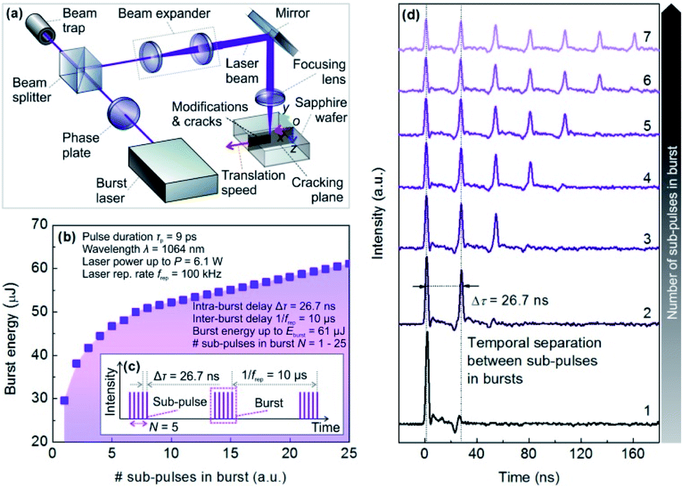 | ||
| Fig. 1 (a) Experimental setup for initiation of modifications (cracks) in moving sapphire wafer by using bursts of laser pulses. (b) Burst energy versus burst length at 100 kHz inter-burst repetition rate. (c) Schematic representation of temporal intensity profile of the laser burst mode irradiation at a burst length of 5. (d) Oscilloscope traces of picosecond laser pulse bursts at different numbers of sub-pulses in bursts ranging from 1 to 7. | ||
The laser power was controlled by using an external attenuator which consisted of a polarizing beam splitter cube, half-wave phase plate. The beam trap was installed for safety reasons in order to collect the unwanted laser irradiation passing through polarizing beam splitter cube. The beam diameter was enhanced by using a beam expander with the magnification factor of 4, composed of concave and convex lenses with focal lengths of −25 mm and +100 mm, respectively. The expander was also used for the collimation of the beam. The Gaussian laser beam was directed to the sapphire wafer by using a high reflective mirror and focused inside the volume of the sapphire by using the aspheric objective lens (C240TME-1064, Thorlabs) with the numerical aperture (NA) of 0.50 and focal length of F = 8.0 mm. The diameter of the collimated beam of D = 5.7 mm on the entrance of focusing objective lens was measured by the knife-edge technique.52,53 The laser transverse spot size of the focused beam inside the volume of sapphire was evaluated by using classical equation w0 = (2M2λF)/(πD). The spot size radius of the Gaussian beam was of w0 = 1.0 μm and the Rayleigh length of zR ≈ 3.0 μm. The sapphire was translated with the direction of speed perpendicular to the beam propagation axis. The linear stages (ALS10020, Aerotech) equipped with software-based machine controllers (A3200, Aerotech) were used for vertical movement of the sample with a speed up to 800 mm s−1. Translation of the wafer at a controllable speed provided the adjustable distance between the transverse beams spots focused inside the volume of sapphire. The motion of the sample was programmed by G-code. The three-dimensional Cartesian coordinate system x, y, z denoted by red, green, blue dotted arrows, respectively, and center point o, given Fig. 1(a), was used to describe the orientation of the sample: beam propagation direction parallel to oz axis, wafer translation direction parallel to ox axis, cracking plane xoz, the top surface of sapphire wafer xoy plane. The same coordinate system was used in all images of the paper. The laser source was capable of generating sequences of laser pulses from 1 to 25 sub-pulses in a burst. The laser power meter (Nova II, Ophir) with sensor (30A-BB-18, Ophir) was employed to measure the irradiation power. The energy of burst was calculated by dividing measured laser power by the inter-burst repetition rate. The burst energy dependence on the number of the sub-pulses in the bursts at 100 kHz repetition rate is given in Fig. 1(b). The burst energy increased with an increasing number of sub-pulses in the burst. The maximal burst energy was always used for the initiation of modification (cracking) in sapphire. The aim of the research was to utilize all available power of laser irradiation source and reach maximum dicing speed. Schematic illustration of the laser burst mode irradiation in intensity versus time representation and the definitions of terms that characterize the burst mode in laser micromachining is given Fig. 1(c). Each of the vertical violet lines represents one sub-pulse in the burst. Tree bursts separated by inter-burst distance 1/frep = 10 μs are shown. Each of the burst consists of 5 sub-pulses, separated by the intra-burst delay Δτ = 26.7 ns. The digital oscilloscope (TDS2012, Tektronix) and photo-detector (PDA30G, Thorlabs) was used to record traces of the bursts of the picosecond laser at various numbers of sub-pulses in the bursts ranging from 1 to 7 depicted in Fig. 1(d). The measured temporal distance between the sub-pulses of 26.7 ns was the same as declared by the laser manufacturer. The next sub-pulse in the burst was always smaller in its intensity than the previous one. Therefore, the sub-pulse intensity in the sequence of the burst gradually decreased.
Synthetic single crystal sapphire (α-Al2O3) wafers with a thickness of 430 μm, a diameter of 50.8 mm, double-sided polished, top surface roughness Ra ≤ 0.3 nm, and bottom surface roughness Ra ≤ 0.5 nm were used in the experiments. Crystallographic orientation notches: off-cut 0.30 deg to M-plane, orientation C-plane (0001), and primary flat orientation A-plane.
2.2. Transverse and longitudinal modification characterization
The optical microscopy was employed for the characterization of transverse and longitudinal laser-induced modification (cracks) inside the volume of sapphire. Diameters and depths of modifications created by the single pulse and burst regimes in sapphire for determination of transverse crack length and longitudinal modification height have been performed by an optical microscope (Eclipse LV100, Nikon) equipped with high-definition 5-megapixel charge-coupled device camera (DS-Fi1, Nikon) having a resolution of 2560 × 1920 pixels. The digital camera was controlled by a controller (Digital Sight DS-U2, Nikon) and image processing software (NIS-Elements D, Nikon). The objective (LU Plan Fluor 20×, Nikon) with a NA = 0.5 and a magnification factor of 20× was used in the bright field. The specimen was illuminated by a halogen lamp (LV-HL50PC, Nikon). The open-source free software Gwyddion was used for image analysis and evaluation of the average length of a transverse crack in xoy plane.The longitudinal modification height in xoz plane has been experimentally measured by the fine-focus knob method.54 The technique relies on the measurement of the top and bottom positions of the laser initiated modification (crack), using the micrometer markings on the fine-focus knob of the optical microscope. Our microscope was equipped with xyz stage (LV-S64, Nikon) and a 100× objective (LU Plan Fluor 100×, Nikon) with NA = 0.9 and 0.2 μm depth of field. The accuracy of longitudinal measurements of the fine-focus knob was 1 μm which was five times larger than the depth of field. Therefore, measurement limitations of modification heights in sapphire were determined by the accuracy of the fine-focus knob. The standard deviation of 10 longitudinal and transverse modifications (cracks) initiated by the same processing parameters was recorded as a measurement error.
3. Results and discussion
3.1. Volume modification by a single burst
The laser beam was focused inside the bulk of sapphire, and single bursts (one sequence of picosecond sub-pulses) were used to induce intra-volume modifications (cracks) in stationary (non-moving) sapphire with control of the number of sub-pulses in a burst from 1 to 25. The optical microscope images of the cracks (transverse xoy plane) induced by single bursts at the various burst lengths are shown in Fig. 2(a). | ||
| Fig. 2 (a) Transverse xoy plane optical microscope images of modifications and cracks induced by a single laser burst inside the volume of sapphire. The numbers under each picture indicate the length of the burst (the number of sub-pulses in a burst). The numbers above each crack indicate the burst energy, average peak pulse intensity in sub-pulse, and total burst fluence. The scale bar on the left image is the same for all pictures. (b) Transverse crack length (xoy plane) versus a number of sub-pulses in a burst. (c) Longitudinal modification height (xoz plane) versus a number of sub-pulses in a burst. Top scales indicate average peak pulse intensity in sub-pulse (red) and total burst fluence (blue) in (b) and (c). | ||
The single bursts induced modifications starting from 1 sub-pulse and ending with 13 sub-pulses in the bursts. By using bursts with lengths from 14 to 25 the modification we not observed. The total burst fluence was evaluated by expression Fburst = 2Eburst/(πw02), where is the Eburst energy, w0 = 1.0 μm Gaussian beam radius at 1/e2 level. The average peak pulse intensity was evaluated by equation Ipulse = Fburst/(Nτp), where N the number of sub-pulses in a burst, τp = 9 ps is the sub-pulse duration. For single pulse (N = 1) irradiation peak pulse intensity was of Ipulse = 0.21 PW cm−2 which is in good agreement with literature value of sapphire amorphization threshold of 0.25 ± 0.04 PW cm−2 measured for laser with a pulse duration of 7 ps.19 The laser-induced modification of sapphire can be classified as nondestructive reversible phase transitions like photorefractive effect, color-centers, photo-darkening, re-solidification, defects produced at the intensity below the damage threshold and irreversible structural changes as void formations and cracks produced at a high intensity above the optical breakdown threshold.55 In our case, spot-like irreversible modifications were induced by the center of the Gaussian beam surrounded by random star-like cracks. The transverse cracks size was plotted as a function of the burst length Fig. 2(b). The crack length increased linearly with the increasing number of sub-pulses in the burst from 1 to ∼4. The size of the crack was constant for the length of the burst from ∼4 to ∼10. The crack length decreased to zero with the increasing number of sub-pulses from ∼10 to 14. The optimal burst length for the largest transverse crack size was found to be around 4–10 sub-pulses. The crack length depends on both total burst fluence and peak pulse intensity. For the low burst lengths (1–4) it increases as energy dose increases, for the large burst lengths (10–14) it decreases as peak pulse intensity decreases. The vertical modification height versus the burst length is given in Fig. 2(c). Longitudinal crack height (xoz plane) decreased linearly with increasing the number of sub-pulses in the burst. The modification height is proportional to the peak pulse intensity and it increases with it. The largest modification height of ∼160 μm was achieved with a single sub-pulse in the burst.
3.2. Stealth dicing of sapphire by using bursts
The stealth dicing of the sapphire wafer by using bursts of laser pulses was performed. The laser beam was focused inside the volume of the sapphire wafer. The focal position of the beam was close to the bottom surface of the wafer and was not changed. The sample was translated at controllable speeds ranging from 25 mm s−1 to 800 mm s−1 with respect to the focused beam. The direction of the speed was perpendicular to the beam propagation direction. The internal laser modifications and cracks formed a cracking plane in the sapphire wafer. The digital force gauge (FMI-S30A5, Alluris) was used to measure torques required to separate the laser scribed sapphire wafers. The external moment of force <10 mN m was applied and the wafers were broken along the cracking plane. The selection of an optimal number of sub-pulses in the burst for maximum dicing speed and easiest cleavage of the wafer was performed experimentally. The series of experiments were realized having all possible a burst lengths (1–25, step 1) and sapphire moving speeds (25 mm s−1–800 mm s−1). However, the maximum dicing speed of 300 mm s−1 with repeatable cleavage of sapphire was recorded only using burst length of 13. Moreover, wafers were easily separated with all tested speeds from 25 mm s−1 to 300 mm s−1 using momentum up to 10 mN m at 13 sub-pulses in the bursts. By using other burst lengths, repeatable cleavage of sapphire was observed only at random dicing speeds always smaller than 0.3 m s−1. Any other burst length (except 13) resulted in smaller dicing speeds. Therefore, a length of 13 sub-pulses in the burst was chosen for further characterization and imaging of broken sapphire samples. The optical microscope images of the transverse planes of the sapphire wafers after laser dicing at various translation speeds at a burst length of 13 are given in Fig. 3(a).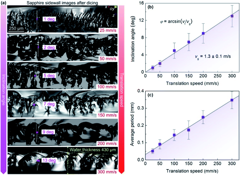 | ||
| Fig. 3 (a) Optical microscope images of a transverse plane of the laser diced and cleaved sapphire by using bursts of picosecond laser pulses. The numbers on the right bottom of each picture indicate the scribing speed ranging from 25 mm s−1 (top) to 300 mm s−1 (bottom). The numbers in the middle of each picture indicate the inclination angle of the modifications. Common processing parameters: laser power 5.5 W; inter-burst repetition rate 100 kHz; burst energy 55 μJ; burst length 13; sapphire wafer thickness 430 μm. The scale bar on the top image is the same for all pictures. (b) The inclination angle of the modification dependence on the translation speed of the sapphire wafer. (c) The modification period dependence on the translation speed of the sapphire wafer. Solid dots represent experimental data points; solid lines are linear fits of the experimental data in (b) and (c). | ||
The periodic array of inclined modifications was observed for all given translation speeds of the sapphire wafer up to 300 mm s−1. The laser-induced modifications started near the bottom of the sapphire. They grew up until reaching the upper plane of the wafer. Then modification stopped forming because the laser beam was defocused near the top surface. The modification was inclined with respect to the beam propagation direction due to sample translation. Dependence of the inclination angle of the modification on the translation speed is given in Fig. 3(b). The inclination angle grows linearly with the increase in the translation speed of the sapphire wafer. After reaching the top part of the wafer and stopping, the process repeated from the beginning, and sapphire was damaged near the bottom plane of the wafer again. Therefore, the modifications were periodical or quasi-periodical. The average period of the cracks versus the translation speed is given in Fig. 3(c). The crack period is linearly proportional to the translation speed of the sapphire wafer. For sapphire wafer moving at 100 mm s−1 speed the period of inclined modifications is 150 μm (see Fig. 3(c)). Therefore the time required to form one single inclined modification is 1.5 ms. Therefore, laser, firing at frep = 100 kHz inter-burst repetition rate (temporal distance between laser bursts τ = 10 μs), fires 150 laser bursts during this interval. Thus, one inclined modification is formed by 150 laser bursts with a total number of 1950 sub-pulses for sapphire traveling at 100 mm s−1. The constant pulse number of ≈150 bursts per one inclined modification is obtained for all the wafer translation speeds (25 mm s−1–300 mm s−1).
The dicing process using burst irradiation has the advantage in comparison to regular pulsed irradiation. The inclined zigzag modifications are observed only with bursts, and not observed by single laser pulses. The inclined modifications are induced in the majority of the area of the transverse cracking plane, which makes easy separation of sapphire wafer possible. The optimal wafer separation achieved in our work for a sapphire with a thickness of 430 μm was 13 sub-pulses in the burst and maximum dicing speed of 300 mm s−1. To our knowledge, we have achieved world record laser dicing speed for 430 μm thick sapphire. The literature review and comparison of laser dicing speeds for sapphire is given in Table 1.
| Dicing speed | Sapphire thickness | Laser power | Pulse duration | Repetition rate | Irradiation type | Beam type | Reference |
|---|---|---|---|---|---|---|---|
| 2.5 mm s−1 | 430 μm | 1.2 W | 0.9 ps | 20 kHz | Pulsed | Bessel | 56 |
| 10 mm s−1 | 400 μm | 8.0 W | 180 ps | 1 MHz | Pulsed | Gaussian | 57 |
| 50 mm s−1 | 430 μm | 7.0 W | 0.9 ps | 100 kHz | Pulsed | Bessel | 56 and 58 |
| 150 mm s−1 | 430 μm | 6.8 W | 10 ps | 100 kHz | Two-color double-pulse | Gaussian | Our previous work27 |
| 300 mm s−1 | 430 μm | 5.5 W | 9 ps | 100 kHz | Burst | Gaussian | This work |
The maximum dicing speed of 300 mm s−1 for 430 μm thick sapphire achieved in this research using burst mode irradiation (9 ps, 5.5 W, 100 kHz) 2 times exceeded closest dicing speed of 150 mm s−1 achieved for the sapphire wafer with same thickness using picosecond dual-wavelength double-pulse irradiation (10 ps, 6.8 W, 100 kHz) patented59 and reported in our previous work.27 The enhancement of dicing speed by the factor of 2 using less powerful laser and the much simpler experimental setup is a promising result for industrial stealth dicing application by bust mode picosecond laser. Dicing speed achieved in our work was 6 times higher than the speed of 50 mm s−1 recorded by sub-picosecond Bessel beam (0.9 ps, 7.0 W, 100 kHz).56,58 The improvement by the factor of 6 using less powerful laser and ten times longer pulse duration is the perspective achievement of stealth dicing technology. The developed process of transparent wafer dicing by using laser bursts and inclined modifications was patented.60
The significance of the spatial zigzag evolution of cracks is important to the separation of the sapphire wafer, as the inclined modifications and cracks take place in the majority of the cross-sectional area of the dicing plane. It has advantages over the well-known dicing scenarios using diverging Gaussian and non-diffracting Bessel beams. In the first dicing scenario, using a tightly focused Gaussian beam with its related limited Rayleigh length the non-inclined modifications with small modification height are formed, thus, several passes through the material are needed what limits the total dicing speed by the same factor.27 In the second dicing scenario, using non-diffracting Bessel beams, modifications over the whole height of the wafer are formed. However, by having a modification made by a single pulse, taking place overall height of wafer, the second modification feels previous modification and affects the propagation of the Bessel beam from top to bottom of the wafer. Therefore, the processing using the Bessel beams is not straight forward, even knowing that these are known for its unique self-reconstruction after passing obstacles in their way. The smart usage of elliptical Bessel beams and control of the crack propagation direction is one possible way of efficient dicing of transparent wafers.61,62
The crack's growth is an essential factor for stealth dicing and separation of sapphire wafers. In our case, the central modification part is surrounded by cracks, which partially scatters the beam. The scattering occurs, especially with the stationary sample and single burst irradiation (Fig. 2). However, by moving sample at controllable speed, the new incoming pulses escape cracks initiated by previous pulses and avoids light scattering by interacting with the undamaged sapphire. The crack formation and propagation direction depend on the crystallographic orientation for sapphire.39 Thus, the scribing direction should influence the efficiency of cracking plane formation. Nevertheless, we have tried our dicing technique over different scribing directions and dicing worker for all tested cases. The maximum crack length and its related total dicing width were always less than 25 μm.
The results in our research were achieved only using the C-plane sapphire. This type of wafer is the most used worldwide, therefore it was chosen for our experiments. We have not tested other types of sapphire (A-plane, M-plane, and R-plane). We expect similar results for other types of sapphire wafers, however, in order to confirm, additional experiments need to be conducted.
3.3. Model of spatial zigzag modification evolution
The model of the spatial evolution of inclined modifications in moving sapphire initiated by bursts of picosecond laser pulses is given in Fig. 4(a). | ||
| Fig. 4 (a) The model of the spatial evolution of inclined cracking in moving sapphire wafer initiated by the focused laser beam and burst irradiation with an indicated sequence of physical processes causing the modification growth at the inclination angle. (b) Geometrical illustration of the periodical zigzag formation of modifications and cracks in translated sapphire initiated by focused Gaussian beam and picosecond laser bursts. (c) Illustration of inclination angle increase with an increase of wafer translation speed. The vg is the modification growth speed vector, vt is the horizontal sample translation speed vector, φ is the modification inclination angle in (a–c). The inclination angle increases φ1 > φ2 > φ3 with increasing translation speed vt1 > vt2 > vt3 in (c). | ||
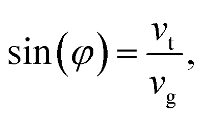
The side view of the sapphire cracking plane is shown in Fig. 4(a). The first burst of focused Gaussian laser beam initiates the modification at the height of the focus position close to the bottom of the sapphire wafer. The modification induced by the first laser burst is shown by a yellow dotted line with a circular shape. The modification front grows at the thermal propagation speed. The laser modified zone is of enhanced absorption because of induced color centers in sapphire. The shifted beam of the second burst interacts with an enhanced absorption zone and is absorbed even beam is de-focused at the higher part of the sapphire wafer. The modification zone initiated by the second burst also grows at thermal propagation speed. The following shifted defocused beam of the third burst interacts with an enhanced absorptivity zone of the second burst. The modification initiated by the third burst also grows at thermal propagation speed. Therefore, it allows for the modification to grow upwards in the constant inclined direction. However, in reality, the modification pattern moves upwards in a curved line with the inclination angle dependable on the vertical position as experimentally observed in Fig. 3(a). The variation of inclination angle along vertical position is related to the decrease of laser fluence of Gaussian beam with increasing distance from focus since it was focused at the bottom of the sapphire wafer. In order to have a simple geometrical illustration of the proposed model, we have used the constant inclination angle. The inclination angle φ of modification in respect to the beam propagation direction has geometrical relation to the sample translation speed vector vt and modification growth speed vector vg. The sapphire wafer translation speed in respect of stationary focused Gaussian beam is given by a red arrow. The modification growth speed is given by cyan arrow. The modification grows at thermal wave propagation speed in all xyz directions and forms a sphere with radius vg/frep until following laser burst is fired, where frep inter-burst repetition rate. The modification front with enhanced absorptivity meets the next beam at ox position shifted by distance vt/frep. The sinus of the inclination angle can be evaluated from the right triangle geometry formed by vt and vg vectors:
 | (1) |
Similar to the spatial zigzag evolution of cracks observed in our work, the dynamic plasma motion in internal modification of glass by fs-laser pulses at a high pulse repetition rate has been reported.66 It was explained by the evolution of free-electron density in internal modification based on the rate equation model, which was coupled with the thermal conduction model in order to incorporate the effect of thermal ionization.67 The model showed that highly absorbing small plasma generated near the geometrical focus moves toward the laser source periodically to cover the region, which is much larger than focus volume.67 This phenomenon was recently confirmed experimentally during the welding of glass by femtosecond laser pulse bursts.68
4. Conclusions
In this work, volume modifications and cracks in the sapphire wafer were initiated by irradiation of successions of picosecond laser pulses (bursts). Laser irradiation source generated bursts of pulses with controlled length from 1 to 25 sub-pulses in a burst. The Gaussian laser beam was tightly focused inside the bulk of transparent sapphire. The total burst energy grew with an increasing number of sub-pulses. The temporal distance between sub-pulses in the burst was kept constant at 26.7 ns.The laser irradiation with a single burst at a variable number of sub-pulses from 1 to 13 initiated internal modifications and cracks inside the volume of sapphire. The largest sizes of transverse cracks were achieved by using bursts with ∼4–10 sub-pulses. The highest longitudinal modification was observed at 1 sub-pulse in a burst.
The spatial zigzag evolution of modifications and cracks was observed when the wafer was translated at a controllable speed perpendicularly to the beam propagation direction. All possible combinations of translations speeds and burst lengths have been tested. The cleavage of the scribed sapphire wafer after applying moment of force up to 10 mN m was achieved only using 13 sub-pulses in a burst and all tested translation speeds from 25 mm s−1 to 300 mm s−1. The analysis of the crack plane revealed periodical repetition of inclined modifications and cracks which took the majority of cross-section and caused repeatable wafer separation. The period of the modifications and the inclination angle had a linear dependence on the translation speed.
The model of spatial zigzag evolution of inclined periodical modification formation was created in order to explain experimental results. The modification growth speed of 1.3 ± 0.1 m s−1 evaluated from experimental data fit by model equation and have good agreement with thermal propagation speed in sapphire. The newly observed effect of inclined modifications inside the volume of sapphire initiated by bursts of picosecond laser pulses was used for stealth dicing of the wafer. The maximal dicing speed of 300 mm s−1 for a sapphire with a thickness of 430 μm was demonstrated by burst mode laser with average power 5.5 W, inter-burst repetition rate 100 kHz, sub-pulse duration 9 ps, the temporal distance between sub-pulses 26.7 ns, and a number of sub-pulses 13.
Funding
Research Council of Lithuania (LMT) (TEC-07/2015).Conflicts of interest
The authors declare that there are no conflicts of interest related to this article.Acknowledgements
We acknowledge laser manufacturing company Ekspla and Dr Nerijus Rusteika for giving us the opportunity to make scientific research using the state-of-the-art picosecond burst laser.References
- M. Yoshimoto, K. Yoshida, H. Maruta, Y. Hishitani, H. Koinuma, S. Nishio, M. Kakihana and T. Tachibana, Nature, 1999, 399, 340–342 CrossRef CAS.
- P. Dragic, T. Hawkins, P. Foy, S. Morris and J. Ballato, Nat. Photonics, 2012, 6, 627–633 CrossRef.
- R. Yamauchi, Y. Hamasaki, T. Shibuya, A. Saito, N. Tsuchimine, K. Koyama, A. Matsuda and M. Yoshimoto, Sci. Rep., 2015, 5, 14385 CrossRef CAS.
- A. Tanaka, R. Chen, K. L. Jungjohann and S. A. Dayeh, Sci. Rep., 2015, 5, 17314 CrossRef CAS.
- H. Liu and D. Chi, Sci. Rep., 2015, 5, 11756 CrossRef CAS.
- G. Li, W. Wang, W. Yang, Y. Lin, H. Wang, Z. Lin and S. Zhou, Rep. Prog. Phys., 2016, 79, 056501 CrossRef.
- S. K. Saha, R. Kumar, A. Kuchuk, M. Z. Alavijeh, Y. Maidaniuk, Y. I. Mazur, S. Q. Yu and G. J. Salamo, Cryst. Growth Des., 2019, 19, 5088–5096 CrossRef CAS.
- H. Zhu, L. A. Tessaroto, R. Sabia, V. A. Greenhut, M. Smith and D. E. Niesz, Appl. Surf. Sci., 2004, 236, 120–130 CrossRef CAS.
- T. Vodenitcharova, L. C. Zhang, I. Zarudi, Y. Yin, H. Domyo, T. Ho and M. Sato, J. Mater. Process. Technol., 2007, 193, 52–62 CrossRef.
- R. R. Gattass and E. Mazur, Nat. Photonics, 2008, 2, 219–225 CrossRef CAS.
- R. W. Dreyfus, F. a. McDonald and R. J. von Gutfeld, Appl. Phys. Lett., 1987, 50, 1491 CrossRef CAS.
- D. Ashkenasi, A. Rosenfeld, H. Varel, M. Wähmer and E. E. B. Campbell, Appl. Surf. Sci., 1997, 120, 65–80 CrossRef CAS.
- H. Horisawa, H. Emura and N. Yasunaga, Vacuum, 2004, 73, 661–666 CrossRef CAS.
- X. C. Wang, G. C. Lim, H. Y. Zheng, F. L. Ng, W. Liu and S. J. Chua, Appl. Surf. Sci., 2004, 228, 221–226 CrossRef CAS.
- O. Uteza, B. Bussiere, F. Canova, J. Chambaret, P. Delaporte, T. Itina and M. Sentis, Appl. Surf. Sci., 2007, 254, 799 CrossRef CAS.
- B. Bussière, N. Sanner, M. Sentis and O. Utéza, Sci. Rep., 2017, 7, 1249 CrossRef.
- D. Nieto, J. Arines, G. M. O'Connor and M. T. Flores-Arias, Appl. Opt., 2015, 54, 8596 CrossRef CAS.
- G. Eberle, M. Schmidt, F. Pude and K. Wegener, Appl. Surf. Sci., 2016, 378, 504 CrossRef CAS.
- L. C. Apuano, R. P. Ohl, R. M. T. Iggelaar, J. W. B. Erenschot, G. E. G. Ardeniers and G. R. B. E. R. Ömer, Opt. Express, 2018, 26, 29283 CrossRef.
- M. Kumagai, N. Uchiyama, E. Ohmura, R. Sugiura, K. Atsumi and K. Fukumitsu, IEEE Trans. Semicond. Manuf., 2007, 20, 259–265 Search PubMed.
- W.-S. Lei, A. Kumar and R. Yalamanchili, J. Vac. Sci. Technol., 2012, 30, 040801 CrossRef.
- W. H. Teh, D. S. Boning and R. E. Welsch, IEEE Trans. Semicond. Manuf., 2015, 28, 408–423 Search PubMed.
- E. Ohmura, F. Fukuyo, K. Fukumitsu and H. Morita, Int. J. Comput. Mater. Sci. Surf. Eng., 2007, 1, 677 CAS.
- Y. Zhang, H. Xie, H. Zheng, T. Wei, H. Yang, J. Li, X. Yi, X. Song, G. Wang and J. Li, Opt. Express, 2012, 20, 6808 CrossRef CAS.
- K. H. Lee, H. J. Park, S. H. Kim, M. Asadirad, Y.-T. Moon, J. S. Kwak and J.-H. Ryou, Opt. Express, 2015, 23, 20340 CrossRef CAS.
- P. C. Verburg, G. R. B. E. Römer and A. J. Huis In ’t Veld, Opt. Express, 2014, 22, 21958 CrossRef CAS.
- M. Gedvilas, J. Mikšys, J. Berzinš, V. Stankevič and G. Račiukaitis, Sci. Rep., 2017, 7, 5218 CrossRef.
- S. Butkus, D. Paipulas, R. Sirutkaitis, E. Gaižauskas and V. Sirutkaitis, J. Laser Micro/Nanoeng., 2014, 9, 213–220 CrossRef CAS.
- D. Kiselev, L. Woeste and J. P. Wolf, Appl. Phys. B: Lasers Opt., 2010, 100, 515–520 CrossRef CAS.
- A. Couairon and A. Mysyrowicz, Phys. Rep., 2007, 441, 47–189 CrossRef CAS.
- W.-J. Tsai, C.-J. Gu, C.-W. Cheng and J.-B. Horng, Opt. Eng., 2013, 53, 051503 CrossRef.
- L. Rapp, R. Meyer, R. Giust, L. Furfaro, M. Jacquot, P. A. Lacourt, J. M. Dudley and F. Courvoisier, Sci. Rep., 2016, 6, 34286 CrossRef CAS.
- O. Brzobohatý, T. Cizmár and P. Zemánek, Opt. Express, 2008, 16, 12688–12700 CrossRef.
- Z. Du, L. Chen, T. S. Kao, M. Wu and M. Hong, Beilstein J. Nanotechnol., 2015, 6, 1199–1204 CrossRef CAS.
- J. M. D. M. K. Bhuyan, F. Courvoisier, P.-A. Lacourt, M. Jacquot, R. Salut and L. Furfaro, Appl. Phys. Lett., 2010, 97, 081102 CrossRef.
- F. C. J. Zhang, M. K. B. M. Jacquot and J. M. Dudley, Appl. Phys. A, 2013, 112, 29–34 CrossRef.
- M. K. Bhuyan, F. Courvoisier, H. S. Phing, O. Jedrkiewicz and S. Recchia, Eur. Phys. J.: Spec. Top., 2011, 199, 101–110 CAS.
- S. A. M. Itra, M. A. C. Hanal, R. A. C. Lady, A. L. M. Ouskeftaras and D. A. G. Rojo, Appl. Opt., 2015, 54, 7358–7365 CrossRef.
- L. Rapp, R. Meyer, L. Furfaro, C. Billet, R. Giust and F. Courvoisier, Opt. Express, 2017, 25, 9312 CrossRef CAS.
- A. Yadav, H. Kbashi, S. Kolpakov, N. Gordon and K. Zhou, Appl. Phys. A, 2017, 123, 369 CrossRef.
- Y. Takiguchi, M. Oyaizu, M. Nakano, T. Inoue and T. Haruyoshi, Opt. Eng., 2018, 56, 077109 CrossRef.
- H. Kalaycıoğlu, Ö. Akçaalan, S. Yavaş, Y. B. Eldeniz and F. Ö. Ilday, J. Opt. Soc. Am. B, 2015, 32, 900 CrossRef.
- H. Pan, R. Yan, X. Fa, X. Yu, Y. Ma, R. Fan, X. Li, D. Chen and Z. Zhou, Opt. Rev., 2016, 23, 386–390 CrossRef CAS.
- C. Kerse, H. Kalayc, P. Elahi, S. Yava, D. K. Kesim, Ö. Akçaalan, S. Yavaş, M. D. Aşık, B. Öktem, H. Hoogland, R. Holzwarth and F. Ö. Ilday, Nature, 2016, 537, 84–88 CrossRef CAS.
- C. Emmelmann and J. P. C. Urbina, Phys. Procedia, 2011, 12, 172–181 CrossRef.
- Y. Ren, C. W. Cheng, J. K. Chen, Y. Zhang and D. Y. Tzou, Int. J. Therm. Sci., 2013, 70, 32–40 CrossRef CAS.
- C. Javaux Léger, K. Mishchik, O. Dematteo-Caulier, S. Skupin, B. Chimier, G. Duchateau, A. Bourgeade, C. Hönninger, E. Mottay, J. Lopez and R. Kling, Proc. SPIE, 2015, 9351, 93510M CrossRef.
- M. Lapczyna, K. P. Chen, P. R. Herman, H. W. Tan and R. S. Marjoribanks, Appl. Phys. A, 1999, 69, 883–886 CrossRef.
- W. Hu, Y. C. Shin and G. King, Appl. Phys. A, 2010, 98, 407–415 CrossRef CAS.
- R. S. Marjoribanks, C. Dille, J. E. Schoenly, L. McKinney, A. Mordovanakis, P. Kaifosh, P. Forrester, Z. Qian, A. Covarrubias, Y. Feng and L. Lilge, Photonics Lasers Med., 2012, 1, 155–169 Search PubMed.
- D. Esser, S. Rezaei, J. Li, P. R. Herman and J. Gottmann, Opt. Express, 2011, 19, 25632–25642 CrossRef CAS.
- Y. Suzaki and A. Tachibana, Appl. Opt., 1975, 14, 2809 CrossRef CAS.
- G. Veshapidze, M. L. Trachy, M. H. Shah and B. D. DePaola, Appl. Opt., 2006, 45, 8197 CrossRef CAS.
- S. Brattgård, J. R. Microsc. Soc., 1954, 74, 113–122 CrossRef.
- E. G. Gamaly, S. Juodkazis, K. Nishimura, H. Misawa, B. Luther-Davies, L. Hallo, P. Nicolai and V. T. Tikhonchuk, Phys. Rev. B, 2006, 73, 214101 CrossRef.
- K. Mishchik, B. Chassagne, C. Javaux-léger, C. Hönninger, E. Mottay, R. Kling and J. Lopez, Proc. SPIE, 2016, 9740, 97400W CrossRef.
- Y. Okamoto, K. Takahashi and A. Okada, Proc. ICALEO, 2012, 2012, 813 Search PubMed.
- J. Lopez, K. Mishchik, B. Chassagne, C. H. Clémentine Javaux-Leger, E. Mottay and R. Kling, Proc. ICALEO, 2015, 2015, 60–69 Search PubMed.
- G. Račiukaitis, M. Gedvilas and V. Stankevič, EP Pat., EP2944412 B1, 2017.
- G. Račiukaitis, M. Gedvilas and S. Mikalauskas, LT Pat., LT6544 B, 2018.
- J. Dudutis, P. Gečys and G. Račiukaitis, Opt. Express, 2016, 24, 28434 CrossRef.
- J. Dudutis, R. Stonys, G. Račiukaitis and G. Paulius, Opt. Express, 2018, 26, 3627 CrossRef CAS.
- E. Marin, Eur. J. Phys., 2013, 34, L83–L85 CrossRef.
- K. Kim and Z. Guo, Proc. IMECE, 2005, 2005, 80873 Search PubMed.
- A. M. Hofmeister, Phys. Chem. Miner., 2014, 41, 361–371 CrossRef CAS.
- I. Miyamoto, Y. Okamoto, R. Tanabe and Y. Ito, Phys. Procedia, 2014, 56, 973–982 CrossRef.
- I. Miyamoto, Y. Okamoto, R. Tanabe, Y. Ito, K. Cvecek and M. Schmidt, Opt. Express, 2016, 24, 10714–10727 Search PubMed.
- S. Hecker, B. Markus, D. Grossmann and T. Graf, Appl. Opt., 2020, 59, 6452–6458 CrossRef.
| This journal is © The Royal Society of Chemistry 2020 |