
 Open Access Article
 This Open Access Article is licensed under a Creative Commons Attribution-Non Commercial 3.0 Unported Licence
Modulation for efficiency and spectra of non-doped white organic light emitting diodes by combining an exciplex with an ultrathin phosphorescent emitter
Zemei Liua,
Bo Zhao *a,
Yuan Gao*b,
Haifeng Chenc,
Bizheng Donga,
Yabo Xua,
Hua Wang*a,
Bingshe Xua and
Wenlian Lid
*a,
Yuan Gao*b,
Haifeng Chenc,
Bizheng Donga,
Yabo Xua,
Hua Wang*a,
Bingshe Xua and
Wenlian Lid
aKey Laboratory of Interface Science and Engineering in Advanced Materials of Ministry of Education, Taiyuan University of Technology, Taiyuan 030024, China. E-mail: zhaobo01@tyut.edu.cn; wanghua001@tyut.edu.cn
bCollege of Economics and Management, Chongqing University of Arts and Sciences, Chongqing 402160, China. E-mail: yuangao@cqwu.edu.cn
cSchool of Electronic Information and Electrical Engineering, Chongqing University of Arts and Sciences, Chongqing 402160, China
dState Key Laboratory of Luminescence and Applications, Changchun Institute of Optics, Fine Mechanics and Physics, Chinese Academy of Sciences, Changchun 130033, China
First published on 10th September 2020
Abstract
Herein, structured non-doped white organic light-emitting diodes (WOLEDs) were designed by combining the emission of a blue exciplex and orange-red phosphorescent ultrathin layer. The device efficiency and spectra were modulated successfully by adjusting the thickness of the exciplex layer and ultrathin layer, respectively. Meanwhile, high efficiency with external quantum efficiency (EQE) ranging from 15% to 22%, power efficiency from 33 lm W−1 to 47 lm W−1 and warm white emission with correlated color temperature (CCT) from 1600 K to 2600 K were realized. The energy transfer process and emission mechanism is also discussed, and the results reveal that the efficient charge trapping and recombination contribute to the improvement of device efficiency and reduce the roll-off efficiency.
1. Introduction
White organic light emitting diodes (WOLEDs) exhibit huge application prospects in lighting fields due to their flexible lighting and natural plane light source. In general, a host–guest doped system is applied in the emitting layer (EML) structure of an OLED to reduce the exciton concentration quenching. Further, blue/orange or blue/green/red emitter-based multi-EMLs have to be used in WOLEDs to produce the white emission. Therefore, WOLEDs often consist of multi-EML host–guest-doped structures, and suffer from fabrication complexity, low repeatability, difficult concentration controllability and hard host material selectivity.1–4 In order to overcome the above-mentioned disadvantages, the structured non-doped WOLED-based ultrathin layers were studied from the past literature.5–8Besides the traditional-fluorescent,9,10 phosphorescent11,12 and thermally activated delayed fluorescence (TADF) emitter13,14 based single molecular emission used in OLEDs, the bi-molecular emission of an exciplex resulting from the intermolecular charge transfer excited state, received significant attention since the discovery of triplet exciton reverse intersystem crossing (RISC) in 2012 by Adachi et al.15 Subsequently, a series of high efficiency exciplex OLED-based blue, green and orange emissions were exploited by harvesting the triplet exciton through the RISC process.16–19 Compared to the single molecular emission materials, exciplex OLEDs present some more advantages such as fluorescence emission with low cost, reduced power loss with low operating voltage and relative small roll-off efficiency with the wide exciton recombination zone. In particular, the low operating voltage benefitted from the barrier-free charge injection contributes to the improvement of the power efficiency and reduce power loss, which is an important parameter for WOLEDs. Therefore, it seems to be a promising method to combine the exciplex with the ultrathin layer to fabricate non-doped WOLEDs. Ying et al. employed an orange ultrathin phosphorescent emitter of Ir(tptpy)2acac to insert into a different location of the blue co-doping exciplex host to achieve highly efficient non-doped WOLEDs.20 Xu et al. fabricated efficient tandem non-doped WOLEDs by inserting blue and orange phosphorescent ultrathin emitters of FIrpic and PO-01, respectively, into the interface of a bi-layer exciplex.21 Feng et al. utilized the energy transfer of a bi-layer exciplex by inserting an orange fluorescent ultrathin emitter of TBRb into the donor or acceptor to earn high efficiency non-doped WOLEDs.22 Although some good results were realized through the combination of co-doping/bi-layer exciplex with ultrathin layer emitter, the influence on the efficiency and spectra of exciplex/ultrathin layer thickness is rarely researched in non-doped WOLEDs. Moreover, highly efficient and highly color stable WOLED-based exciplexes and ultrathin layers still need to be investigated further.
In this work, we designed non-doped WOLEDs by combining the blue exciplex emission of m-bis(N-carbazolyl)benzene:(1,3,5-triazine-2,4,6-triyl) tris(benzene-3,1-diyl) tris(diphenylphosphineoxide) (mCP:PO-T2T) with orange-red ultrathin phosphorescent emitter iridium(III) bis(2-phenylquinoline) acetylacetonate (Ir(pq)2acac) to achieve white light emission. The ultrathin phosphorescent layers were inserted into both sides of the exciplex layer, and the thickness of the ultrathin layer and exciplex layer was adjusted, respectively, to modulate the efficiency and spectra of WOLEDs. As a result, the efficiency and spectra are modulated successfully through the thickness with EQE ranging from 15% to 22%, power efficiency from 33 lm W−1 to 47 lm W−1 and the correlated color temperature (CCT) from 1600 K to 2600 K.
2. Experimental section
All the organic and inorganic materials used in this study were purchased from commercial sources and used without further purification. All OLEDs were fabricated on indium tin oxide (ITO)-coated glass substrates with a sheet resistance of 10 Ω sq−1. The organic layers were deposited at a rate of 1.0 Å s−1, and the inorganic layers of MoO3 and LiF were deposited at a rate of 0.1 Å s−1. An Al cathode was deposited in the end at a rate of 5.0 Å s−1 with a shadow mask, which defined a device area of 3 × 3 mm2. The photoluminescence (PL) spectra were measured using a FluoroMax-4 fluorescence spectrometer (HORIBA Jobin Yvon). The UV-Vis absorption spectrum was recorded using a Hitachi U-3900 scanning spectrophotometer. The electroluminescence (EL) spectra were measured through a computer controlled PR-655 Spectra Scan spectrometer. The current–voltage–luminance curves were measured with Keithley 2400 power supply combined with a BM-7A luminance colorimeter. External quantum efficiency (EQE) was calculated from the current density–voltage–luminance curve and spectral data. Besides, all measurements were carried out at room temperature and under ambient conditions without any protective coatings.3. Results and discussions
3.1 Photo-physical property of the exciplex
In this work, complementary colors of blue and orange-red are adopted to form white emission. mCP and PO-T2T are chosen as the electron donor and acceptor materials, respectively, to form the blue exciplex, and the phosphorescent emitter of Ir(pq)2acac is selected as the orange-red emission ultrathin layer for WOLEDs. Fig. 1a shows the molecular structure of mCP, PO-T2T and Ir(pq)2acac, and Fig. 1b exhibits the PL spectra of mCP, PO-T2T, mCP:PO-T2T mixed films (1![[thin space (1/6-em)]](https://www.rsc.org/images/entities/char_2009.gif) :1) and absorption spectra of Ir(pq)2acac emitters. The observed emission peak of 468 nm is from the mCP:PO-T2T mixed film that is different from the emission of the donor of mCP (365 nm) and acceptor of PO-T2T (381 nm), thus indicating the formation of the exciplex formation. Besides, the peak value of 2.64 eV is similar to the energy gap between the highest occupied molecular orbital (HOMO) of mCP (6.1 eV) and lowest unoccupied molecular orbital (LUMO) of PO-T2T (3.5 eV), which also demonstrates the formation of the exciplex between mCP and PO-T2T. The OLED-based mCP:PO-T2T exciplex also had been reported for highly efficient blue emission, which could reach a high EQE of 8% due to the long-lifetime TADF emission.23 The high efficiency of the exciplex could also provide an efficient blue emission in our WOLEDs. The large overlap between the absorption spectra of the Ir(pq)2acac phosphorescent emitter and the PL spectrum of mCP:PO-T2T exciplex could be observed, and indicate that a high Förster energy transfer efficiency from the exciplex to Ir(pq)2acac could occur.24
:1) and absorption spectra of Ir(pq)2acac emitters. The observed emission peak of 468 nm is from the mCP:PO-T2T mixed film that is different from the emission of the donor of mCP (365 nm) and acceptor of PO-T2T (381 nm), thus indicating the formation of the exciplex formation. Besides, the peak value of 2.64 eV is similar to the energy gap between the highest occupied molecular orbital (HOMO) of mCP (6.1 eV) and lowest unoccupied molecular orbital (LUMO) of PO-T2T (3.5 eV), which also demonstrates the formation of the exciplex between mCP and PO-T2T. The OLED-based mCP:PO-T2T exciplex also had been reported for highly efficient blue emission, which could reach a high EQE of 8% due to the long-lifetime TADF emission.23 The high efficiency of the exciplex could also provide an efficient blue emission in our WOLEDs. The large overlap between the absorption spectra of the Ir(pq)2acac phosphorescent emitter and the PL spectrum of mCP:PO-T2T exciplex could be observed, and indicate that a high Förster energy transfer efficiency from the exciplex to Ir(pq)2acac could occur.24
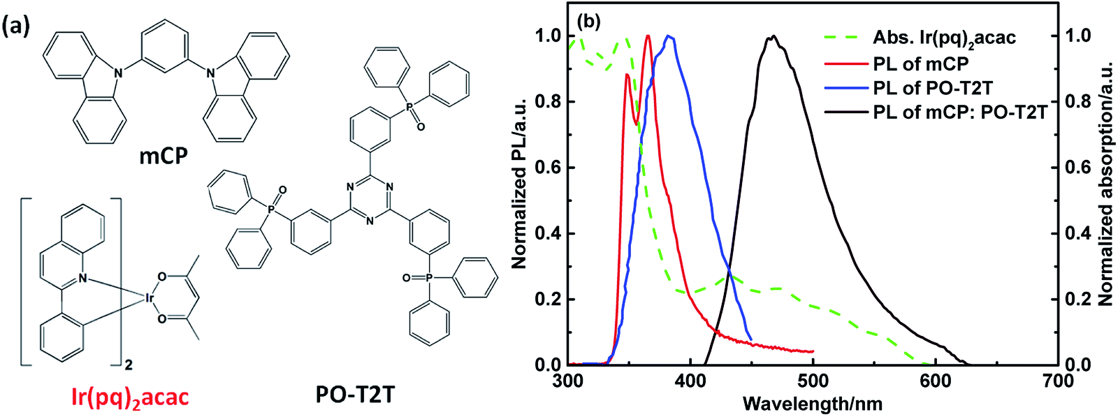 | ||
| Fig. 1 (a) The molecular structure of mCP, PO-T2T and Ir(pq)2acac. (b) The absorption spectrum of Ir(pq)2acac, and PL spectra of mCP, PO-T2T and mCP:PO-T2T mixed film. | ||
3.2 Doped WOLED-based exciplex host
Based on the above-mentioned photo-physical discussion, we first designed a doped WOLED with the device structure of ITO/MoO3 (3 nm)/mCP (30 nm)/mCP:PO-T2T (1:1): x wt% Ir(pq)2acac (15 nm)/PO-T2T (40 nm)/LiF (1 nm)/Al, x = 0.3 and 0.6, and the corresponding WOLED is defined as W0.3 and W0.6, respectively. mCP:PO-T2T (1:1): x wt% Ir(pq)2acac is the EML with exciplex as the host to sensitize Ir(pq)2acac, while mCP and PO-T2T are the hole transport layer (HTL) and electron transport layer (ETL), respectively. The current density, luminance and efficiency characteristic curves are shown in Fig. 2. The WOLED achieves low operation voltages of 3.86 V and 3.71 V under 1000 cd m−2 with W0.3 and W0.6, respectively, and a high luminance of ∼10000 cd m−2. The low operation voltage is a benefit from the barrier-free charge injection from the transport layer to EML due to the same organic materials of HTL/donor and ETL/acceptor. Besides, the charge recombination between the HOMO of mCP and the LUMO of PO-T2T also contributes to the formation of exciplex to reduce the operational voltage.
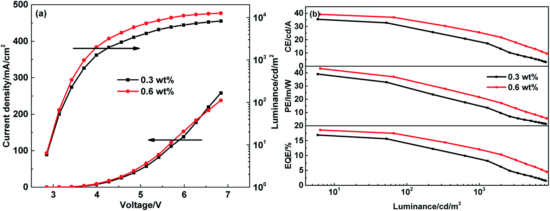 | ||
| Fig. 2 The EL performance of doped structural WOLED. (a) Current density–voltage–luminance curves. (b) CE, PE and EQE–luminance curves. | ||
The maximum current efficiency (CE), power efficiency (PE) and EQE of W0.3 are 35.4 cd A−1, 39.1 lm W−1 and 16.9%, respectively, while the higher efficiency of 39.2 cd A−1, 43.2 lm W−1 and 18.5% are realized with a higher concentration in W0.6. However, the roll-off efficiency from maximum EQE to EQE at 1000 cd m−2 is significant. The EQE of W0.3 at 1000 cd m−2 is 9.0% with the roll-off ratio at 46.7%, and a similar situation occurs in W0.6; the EQE at 1000 cd m−2 is 12.1% and the roll-off ratio is 34.8%. The large roll-off efficiency may arise from high triplet exciton concentration, which results in the significant triplet–triplet annihilation (TTA) and singlet-triplet annihilation (STA). The Dexter energy transfer process from mCP:PO-T2T to Ir(pq)2acac and direct charge trapping recombination in Ir(pq)2acac is difficult to happen due to the low doping concentration; thus, the emission of Ir(pq)2acac is from the Förster energy transfer between the singlet energy level of mCP:PO-T2T and Ir(pq)2acac. Therefore, the RISC in mCP:PO-T2T plays a crucial function and the high RISC efficiency can reduce triplet concentration efficiently. Hence, the serious roll-off efficiency could be considered as high triplet concentration with low RISC efficiency in the mCP:PO-T2T exciplex.23
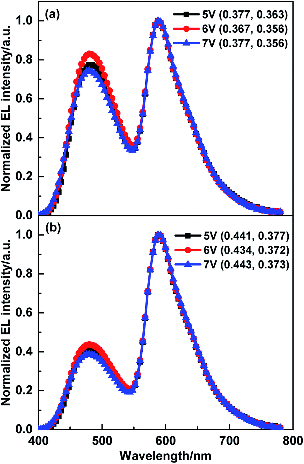
The EL spectra of W0.3 and W0.6 are shown in Fig. 3. The spectra exhibit white emission with two emission peaks of blue emission at 480 nm and orange-red emission at 590 nm, which stem from the mCP:PO-T2T exciplex host and Ir(pq)2acac, respectively. We also did the higher doping concentration; however, the too weak exciplex blue emission impedes the formation of white light emission. Further, as the concentration increases from 0.3 wt% to 0.6 wt%, the exciplex blue emission intensity reduces, and demonstrates efficient energy transfer from the exciplex host to the dopant. The stability Commission Internationale de l'Eclairage (CIE) coordination of (0.367, 0.356) and (0.434, 0.372) at 6 V are also achieved in W0.3 and W0.6, respectively. Hence, the low operation voltage, high efficiency and high color stability WOLED with doped structure of the mCP:PO-T2T exciplex as the host and Ir(pq)2acac as the dopant are realized.
 | ||
| Fig. 3 The EL spectra of doped structural WOLED. (a) 0.3 wt%. (b) 0.6 wt%. | ||
3.3 Non-doped WOLED-based exciplex and ultrathin layer
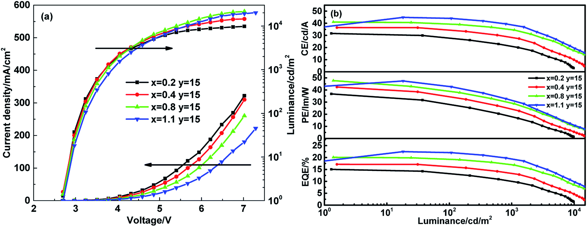
The doped structural WOLED with a low concentration of Ir(pq)2acac in exciplex host of 0.3 wt% and 0.6 wt% suffered from hard concentration precision control and low repeatability. Thus, in this section, we designed the structured non-doped WOLED by combining mCP:PO-T2T exciplex with ultrathin layer Ir(pq)2acac. Further, Ir(pq)2acac ultrathin layers were inserted into both sides of exciplex EML to construct the non-doped WOLED. The device structure of ITO/MoO3 (3 nm)/mCP (30 nm)/Ir(pq)2acac (x nm)/mCP:PO-T2T (1:1) (y nm)/Ir(pq)2acac (x nm)/PO-T2T (40 nm)/LiF (1 nm)/Al was adopted. Here, x = 0.2, 0.4, 0.8, 1.1 and y = 15, and the corresponding WOLED is defined as W0.2/15, W0.4/15, W0.8/15 and W1.1/15, respectively. The mCP:PO-T2T exciplex EML provides the blue emission, and ultrathin layer of Ir(pq)2acac acts as the orange-red emission to form the white emission. Firstly, we fix the exciplex EML thickness as 15 nm, which is same as the thickness of EML in doped WOLED, and the Ir(pq)2acac ultrathin layer is adjusted with four thickness values from 0.2 nm to 1.1 nm.
The current density, luminance and efficiency curves are shown in Fig. 4. Similar to the aforementioned doped WOLED, the non-doped WOLED also achieves a low operation voltage in the range of 3.6–3.8 V at 1000 cd m−2 and high luminance of ∼10000 cd m−2. Although the exciplex layer is separated from the transport layer by inserting the Ir(pq)2acac layer, the ultra-thin thickness from 0.2 nm to 1.1 nm makes the Ir(pq)2acac film discontinuous, which also ensures the efficient charge injection. Therefore, the barrier-free charge injection from transport layer to EML is also suitable for the non-doped WOLED, which results in low operation voltage. However, the reduced current density with increased thickness of ultrathin layer demonstrates the efficient charge trapping by the Ir(pq)2acac emitter. Therefore, we consider that the orange-red emission is mainly from the direct charge trapping recombination by the Ir(pq)2acac molecule rather than the energy transfer from the mCP:PO-T2T exciplex.25,26 The maximum CEs, PEs and EQEs of W0.2/15/W0.4/15/W0.8/15/W1.1/15 shown in Fig. 4b are 31.6/36.5/41.1/44.9 cd A−1, 36.8/42.4/47.7/47.4 lm W−1 and 15.1/17.1/20.1/22.5%, respectively. The peak PE ∼47 lm W−1 satisfies the efficiency requirement of PE > 40 lm W−1 for commercial applications of WOLED. The EQE of ∼20% also reaches the upper limit in phosphorescent WOLED without the optically coupled output structure. While the relatively small roll-off efficiency from maximum EQE to EQE under 1000 cd m−2 with roll-off ratios at 32.9%, 21.6%, 15.2% and 13.4% are also realized, respectively, it is much lower than the doped WOLED with the roll-off ratios of 46.7% and 34.8%. Furthermore, we found that the roll-off ratio decreases from 32.9% to 13.4% with the increased thickness of ultrathin layer. We consider that the direct charge trapping of the Ir(pq)2acac emitter to carrier plays the important role and decreases the carrier injection, recombination and exciton formation in the mCP:PO-T2T exciplex. Therefore, the relative low singlet and triplet exciton concentration in exciplex EML contributes to the reduce of the roll-off efficiency compared to the doped structural WOLED. This means that the roll-off efficiency is mainly derived from the high exciplex exciton concentration quenching rather than the Ir(pq)2acac exciton concentration.
 | ||
| Fig. 4 The EL performance of non-doped structural WOLED with different-thickness ultrathin layers. (a) Current density–voltage–luminance curves. (b) CE, PE and EQE–luminance curves. | ||
The thicker Ir(pq)2acac layer could capture more carriers and improve the orange-red emission intensity, and the EL spectra from W0.2/15 to W1.1/15 are displayed in Fig. 5. All four WOLEDs exhibit pure blue exciplex and orange-red ultrathin layer emission, and just as we expected the blue emission intensity reduces with the enhanced thickness of ultrathin layers. The warm white emission WOLEDs with CIE coordinates of (0.437, 0.365), (0.507, 0.385), (0.535, 0.391) and (0.555, 0.393) at 6 V are realized, and the CCTs ranging from 1600 K to 2600 K are closed for commercial application of warm white light (∼2800 K). As a result, the white emission spectra could be modulated by changing the ultrathin layer thickness.
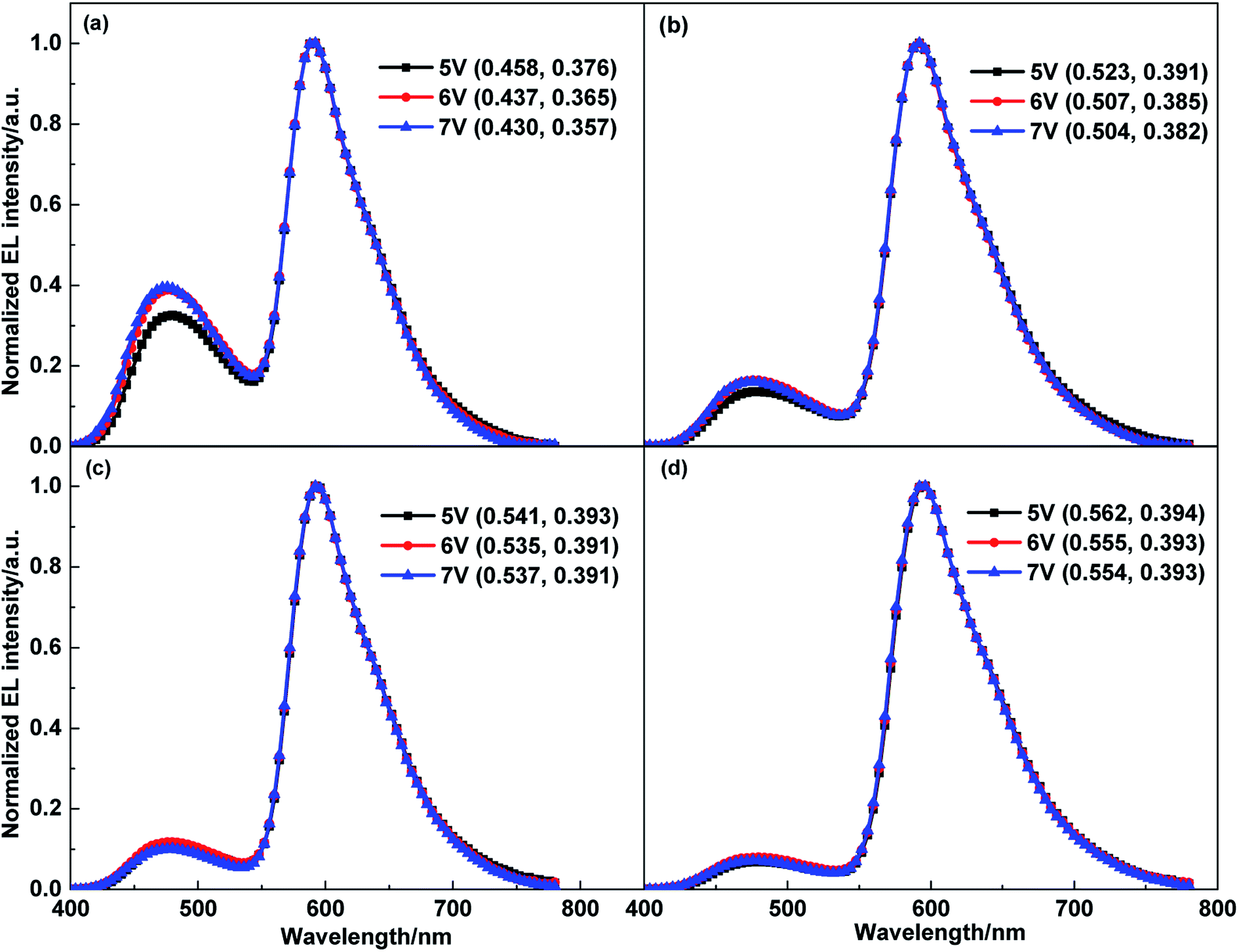 | ||
| Fig. 5 The EL spectra of structured non-doped WOLED with different ultrathin layer thickness. (a) x = 0.2. (b) x = 0.4. (c) x = 0.8. (d) x = 1.1. | ||
Besides the ultrathin layer thickness could adjust the white emission spectra, and we considered that the blue exciplex EML thickness could also be optimized to achieve the modulation for white emission spectra. Thus, in this section, we discuss the same non-doped WOLED structure by fixing the ultrathin layer thickness at 0.8 nm, and exciplex EML thickness at 10, 15, 20 and 25 nm, correspondingly, which is x = 0.8 and y = 10, 15, 20, 25, and the corresponding WOLED is defined for W0.8/10, W0.8/15, W0.8/20 and W0.8/25, respectively. The ultrathin layer thickness of 0.8 nm is adopted due to the high EQE (>20%) and stable white emission spectra in W0.8/15. The EL spectra of WOLED with different exciplex layer thicknesses are shown in Fig. 6. We can see that the blue emission intensity enhances as the exciplex layer thickness increases, which indicates that more charges recombine in the exciplex EML. Meanwhile, the stable white emission spectra are also obtained from W0.8/10 to W0.8/25 with CIE coordinates of (0.568, 0.398), (0.535, 0.391), (0.531, 0.388) and (0.513, 0.380) at 6 V.
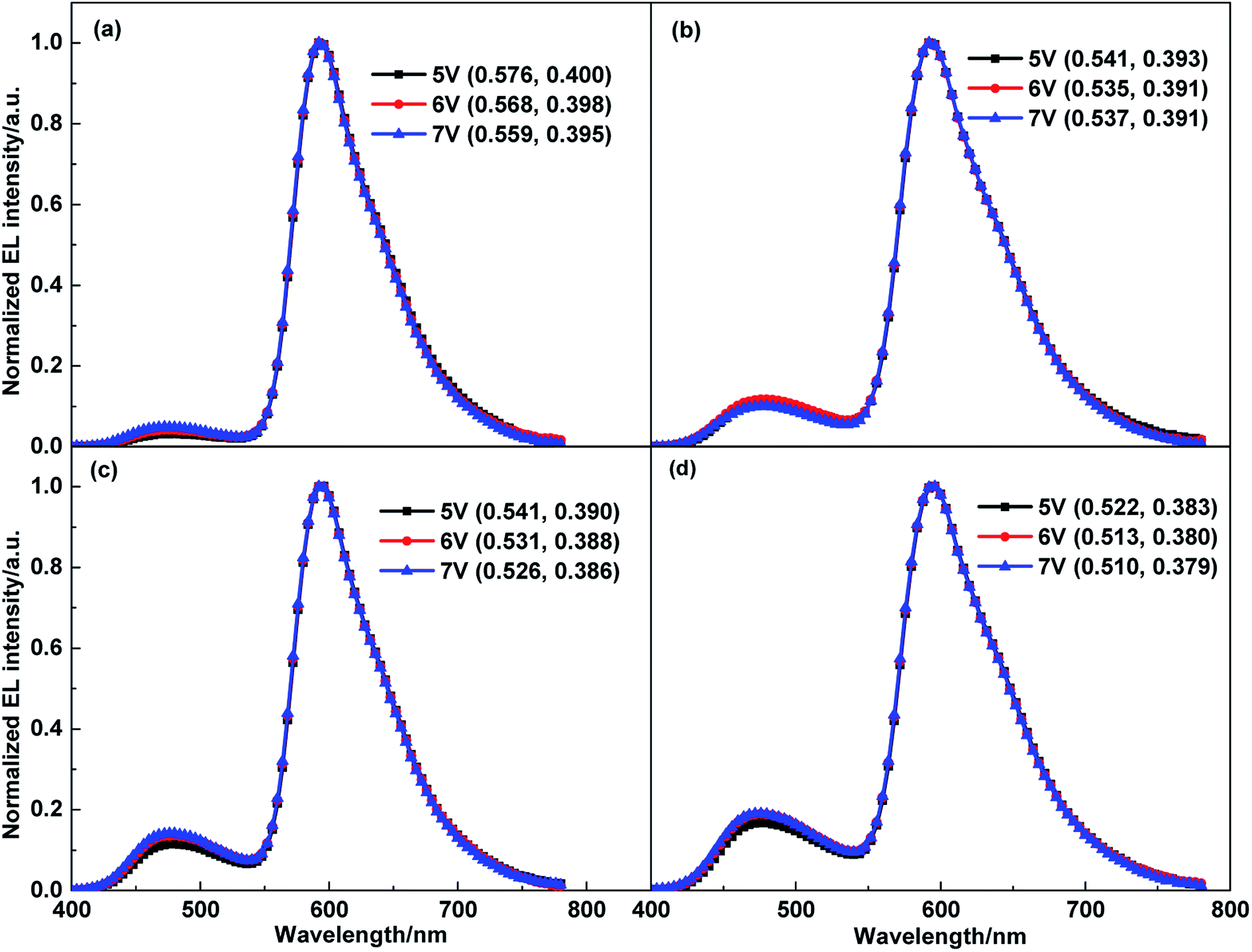 | ||
| Fig. 6 The EL spectra of structured non-doped WOLED with different-thickness exciplex layers. (a) y = 10. (b) y = 15. (c) y = 20. (d) y = 25. | ||
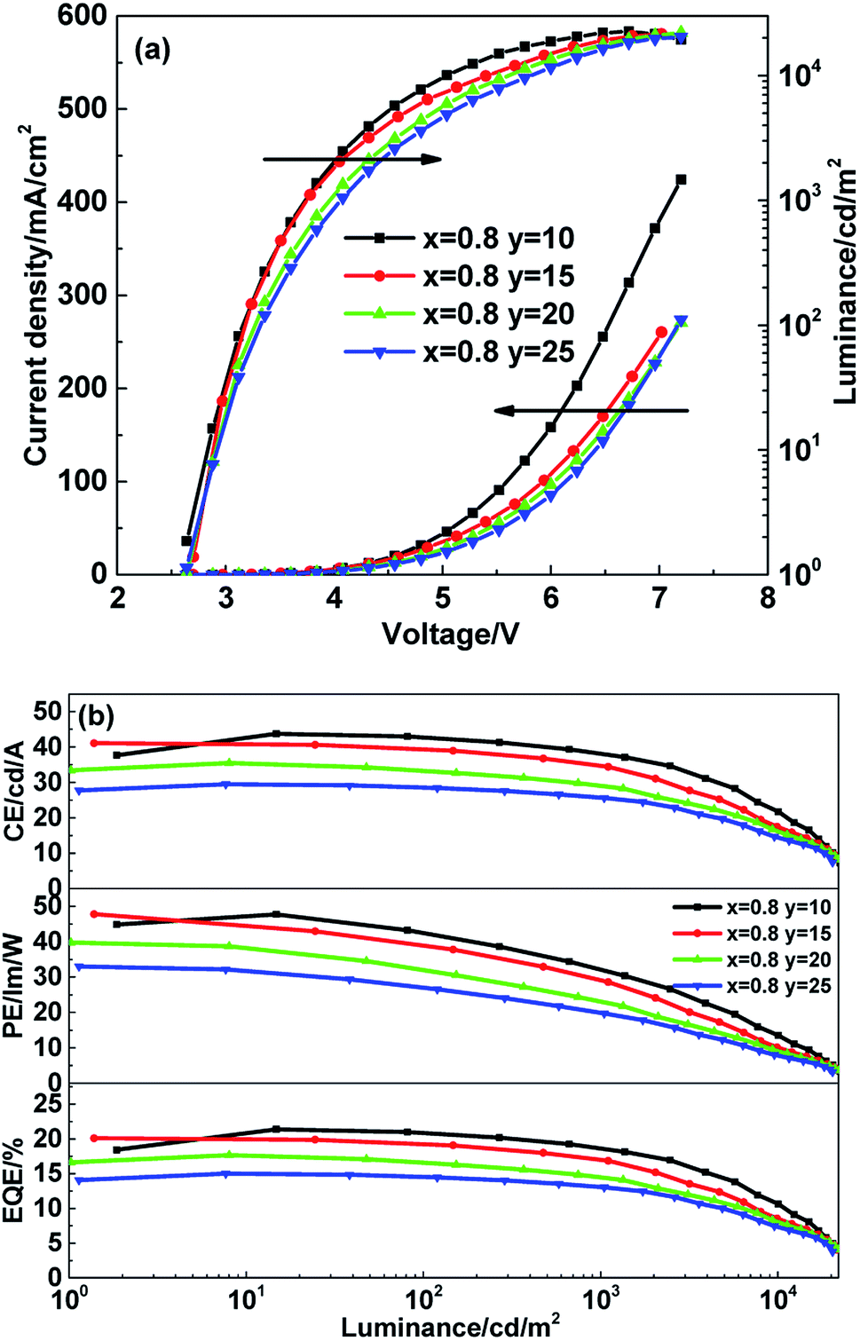
The current density, luminance and efficiency performance curves are exhibited in Fig. 7. It is impressive that all four WOLEDs maintain a low turn-on voltage of ∼2.6 V in spite of the exciplex EML thickness ranging from 10 nm to 25 nm, which means that the charge injection barrier from the transport layer to EML is responsible for the turn-on voltage rather than the EML thickness. Further, a low operation voltage at 1000 cd m−2 for the four WOLEDs is also achieved within the range of 3.7–4.0 V. As discussed above, the barrier-free injection of electrons and holes from the transport layer to EML contribute to the low turn-on voltage and operation voltage. The efficiency curves of W0.8/10/W0.8/15/W0.8/20/W0.8/25 shown in Fig. 7b have maximum CEs, PEs and EQEs with 43.8/41.1/35.5/29.5 cd A−1, 47.7/47.7/39.7/33.0 lm W−1 and 21.4/20.1/17.7/15.0%, respectively. Even at a high luminance of 1000 cd m−2, EQEs still maintain a high value and the roll-off ratios are 12.5%, 15.2%, 17.9% and 12.9%, respectively. Hence, the structured non-doped WOLED discussed here either with different ultrathin layer thickness or different exciplex layer thickness have lower roll-off efficiency than the doped structural WOLED. The direct trapping recombination emission of Ir(pq)2acac molecules in the structured non-doped WOLED reduces the vast exciton formation on the mCP:PO-T2T exciplex and suppresses the energy transfer from the exciplex to Ir(pq)2acac. Therefore, the reduction of the RISC process in the mCP:PO-T2T exciplex helps to weaken TTA and STA, which results in lower roll-off efficiency in the non-doped WOLED than in the doped WOLED. The performances of all WOLEDs in this paper are listed in Table 1.
 | ||
| Fig. 7 The EL performance of structured non-doped WOLED with different-thickness exciplex layers. (a) Current density–voltage–luminance curves. (b) CE, PE and EQE–luminance curves. | ||
| Device | Voltage (V) (103 cd m−2) | CE (cd A−1) (max/103 cd m−2) | PE (lm W−1) (max/103 cd m−2) | EQE (%) (max/103 cd m−2) | Roll-off ratioa | CIE (6 V) | CCT (K) (6 V) |
|---|---|---|---|---|---|---|---|
| a The efficiency roll-off ratio from maximum EQE to EQE at 1000 cd m−2. | |||||||
| W0.3 | 3.86 | 35.4/18.9 | 39.1/15.4 | 16.9/9.0 | 46.7% | (0.367, 0.356) | 4240 |
| W0.6 | 3.71 | 39.2/25.6 | 43.2/21.7 | 18.5/12.1 | 34.8% | (0.434, 0.372) | 2775 |
| W0.2/15 | 3.66 | 31.6/21.3 | 36.8/18.2 | 15.1/10.1 | 32.9% | (0.437, 0.365) | 2653 |
| W0.4/15 | 3.67 | 36.5/28.6 | 42.4/24.6 | 17.1/13.4 | 21.6% | (0.507, 0.385) | 1991 |
| W0.8/15 | 3.73 | 41.1/34.8 | 47.7/29.4 | 20.1/17.0 | 15.2% | (0.535, 0.391) | 1802 |
| W1.1/15 | 3.84 | 44.9/38.9 | 47.4/31.8 | 22.5/19.5 | 13.4% | (0.555, 0.393) | 1678 |
| W0.8/10 | 3.70 | 43.8/38.3 | 47.7/32.4 | 21.4/18.7 | 12.5% | (0.568, 0.398) | 1625 |
| W0.8/15 | 3.73 | 41.1/34.8 | 47.7/29.4 | 20.1/17.0 | 15.2% | (0.535, 0.391) | 1802 |
| W0.8/20 | 3.93 | 35.5/29.2 | 39.7/23.2 | 17.7/14.5 | 17.9% | (0.531, 0.388) | 1811 |
| W0.8/25 | 4.01 | 29.5/25.7 | 33.0/19.9 | 15.0/13.1 | 12.9% | (0.513, 0.380) | 1905 |
In order to further clarify the charge trapping, transport and recombination process in doped and non-doped WOLEDs, we depict the emission schematic in Fig. 8. In the doped structural WOLED, electrons and holes are injected into EML and recombined on the exciplex host to form exciplex singlet and triplet excitons. The direct charge trapping of Ir(pq)2acac and Dexter energy transfer from the exciplex triplet state level to the Ir(pq)2acac triplet state level could be ignored due to the low doping concentration of 0.3 wt% and 0.6 wt%.27 Therefore, the emission of Ir(pq)2acac comes from the long range Förster resonance energy transfer between the singlet state level of the exciplex host and dopant, which could be confirmed from almost the same current density curves of different concentrations, as shown in Fig. 2a. On the other hand, the singlet and triplet excitons of the exciplex host could convert each other through the ISC/RISC process; however, this could also lead to serious roll-off efficiency because of the long excitons lifetime and high excitons concentration.28,29 However, in the non-doped WOLED, the ultrathin layer Ir(pq)2acac in the interface of EML and transport layer could trap the charge efficiently, and the current density decreases with an increase in the thickness of the ultrathin layer, thus demonstrating the direct charge trapping effect. Therefore, the emission of Ir(pq)2acac derives from the direct charge trapping recombination. Due to the charge trapping impact, the charge recombination on the exciplex host reduces and makes the exciplex exciton concentration decrease, which results in the reduced roll-off efficiency in non-doped WOLED compared to the doped WOLED. Therefore, in the structured non-doped WOLED, the white emission is formed from the charge recombination on blue exciplex and direct charge trapping recombination on the orange-red Ir(pq)2acac ultrathin layer.
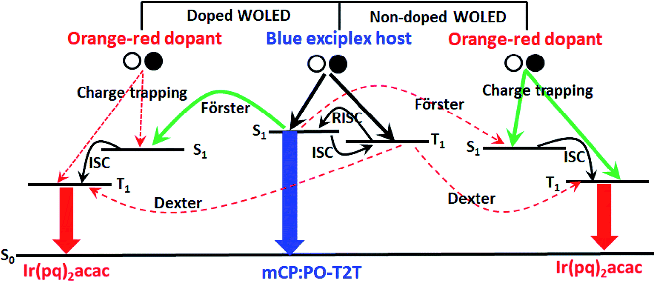 | ||
| Fig. 8 The schematic of the energy transfer process and emission mechanism in doped and non-doped WOLEDs. | ||
4. Conclusion
In summary, doped and structured non-doped WOLEDs through the combination of a blue exciplex and orange-red ultrathin layer are designed successfully. The reduced roll-off efficiency is obtained in the non-doped WOLED in comparison to the doped structure. The modulation for device efficiency and spectra in the non-doped WOLED are also realized through the adjustment of the exciplex EML and ultrathin layer thickness. As a result, the EQE ranging from 15% to 22%, power efficiency from 33 lm W−1 to 47 lm W−1 and CCT from 1600 K to 2600 K are achieved, and the efficient charge trapping and recombination contribute to the improvement of the device efficiency and reduce the roll-off efficiency. We believe that the combination of an exciplex and ultrathin layer would be a promising method to simplify the WOLED structure and improve device performance.Conflicts of interest
There are no conflicts of interest to declare.Acknowledgements
This work was financially supported by National Natural Science Foundation of China (61605137 and 61775155), the publication fee by the Science & Technology Research Program of Chongqing University of Arts and Sciences (R2018SJG21 and R2018SDQ15); the Scientific and Technological Innovation Programs of Higher Education Institutions in Shanxi (STIP, 2020-104).Notes and references
- J. Kido, K. Hongawa, K. Okuyama and K. Nagai, Appl. Phys. Lett., 1994, 64, 815–817 CrossRef.
- B. Zhao, Z. Su, W. Li, B. Chu, F. Jin, X. Yan, F. Zhang, D. Fan, T. Zhang, Y. Gao and J. Wang, Appl. Phys. Lett., 2012, 101, 053310 CrossRef.
- N. Sun, Q. Wang, Y. B. Zhao, Y. H. Chen, D. Z. Yang, F. C. Zhao, J. S. Chen and D. G. Ma, Adv. Mater., 2014, 26, 1617–1621 CrossRef.
- J. Nishide, H. Nakanotani, Y. Hiraga and C. Adachi, Appl. Phys. Lett., 2014, 104, 233304 CrossRef.
- C. Hakim, F. Alexis, F. Sébastien, C. Sébastien, C. Marie-Claude, A. Dominique, S. Alain and G. Bernard, Appl. Phys. Lett., 2006, 89, 183513 CrossRef.
- Y. M. Wang, F. Teng, Z. Xu, Y. B. Hou, S. Y. Yang and X. R. Xu, Mater. Chem. Phys., 2005, 92, 291–294 CrossRef.
- Y. B. Zhao, J. S. Chen and D. G. Ma, ACS Appl. Mater. Interfaces, 2013, 5, 965–971 CrossRef.
- B. Zhao, H. Zhang, Z. Wang, Y. Miao, Z. Wang, J. Li, H. Wang, Y. Hao and W. Li, J. Mater. Chem. C, 2018, 6, 4250–4256 RSC.
- C. W. Tang and S. A. VanSlyke, Appl. Phys. Lett., 1987, 51, 913–915 CrossRef.
- B. Zhao, Y. Miao, Z. Wang, K. Wang, H. Wang, Y. Hao, B. Xu and W. Li, Nanophotonics, 2016, 6, 1133–1140 Search PubMed.
- M. A. Baldo, D. F. O'Brien, Y. You, A. Shoustikov, S. Sibley, M. E. Thompson and S. R. Forrest, Nature, 1998, 395, 151–154 CrossRef.
- B. Tong, Q. Mei, R. Tian, M. Yang, Q. Hua, Y. Shi and S. Ye, RSC Adv., 2016, 6, 34970–34976 RSC.
- H. Uoyama, K. Goushi, K. Shizu, H. Nomura and C. Adachi, Nature, 2012, 492, 234–238 CrossRef CAS.
- J. Li, R. Zhang, Z. Q. Wang, B. Zhao, J. J. Xie, F. Zhang, H. Wang and K. P. Guo, Adv. Opt. Mater., 2018, 6, 1701256 CrossRef.
- K. Goushi, K. Yoshida, K. Sato and C. Adachi, Nat. Photonics, 2012, 6, 253–258 CrossRef CAS.
- T. Y. Zhang, B. Zhao, B. Chu, W. L. Li, Z. S. Su, X. W. Yan, C. Y. Liu, H. R. Wu, F. M. Jin and Y. Gao, Org. Electron., 2015, 25, 6–11 CrossRef CAS.
- W. Liu, J. X. Chen, C. J. Zheng, K. Wang, D. Y. Chen, F. Li, Y. P. Dong, C. S. Lee, X. M. Ou and X. H. Zhang, Adv. Funct. Mater., 2016, 26, 2002–2008 CrossRef CAS.
- Q. T. Siddiqui, A. A. Awasthi, P. Bhui, P. Parab, M. Muneer, S. Bose and N. Agarwal, RSC Adv., 2019, 9, 40248–40254 RSC.
- M. Chapran, P. Pander, M. Vasylieva, G. W. Salyga, J. Ulanski, F. B. Dias and P. Data, ACS Appl. Mater. Interfaces, 2019, 11, 13460–13471 CrossRef CAS.
- S. Ying, J. Yao, Y. Chen and D. Ma, J. Mater. Chem. C, 2018, 6, 7070–7076 RSC.
- T. Xu, J. G. Zhou, M. K. Fung and H. Meng, Org. Electron., 2018, 63, 369–375 CrossRef.
- D. Feng, D. Dong, L. Lian, H. Wang and G. He, Org. Electron., 2018, 56, 216–220 CrossRef.
- W. Y. Hung, G. C. Fang, S. W. Lin, S. H. Cheng, K. T. Wong, T. Y. Kuo and P. T. Chou, Sci. Rep., 2014, 4, 5161 CrossRef.
- Z. Q. Wang, C. Wang, H. Zhang, Z. M. Liu, B. Zhao and W. L. Li, Org. Electron., 2019, 66, 227–241 CrossRef.
- C. Weichsel, L. Burtone, S. Reineke, S. I. Hintschich, M. C. Gather, K. Leo and B. Lüssem, Phys. Rev. B: Condens. Matter Mater. Phys., 2012, 86, 075204 CrossRef.
- L. Zhu, Z. Wu, J. Chen and D. Ma, J. Mater. Chem. C, 2015, 3, 3304–3310 RSC.
- J. H. Lee, S. Lee, S. J. Yoo, K. H. Kim and J. J. Kim, Adv. Funct. Mater., 2014, 24, 4681–4688 CrossRef CAS.
- J. H. Lee, S. H. Cheng, S. J. Yoo, H. Shin, J. H. Chang, C. I. Wu, K. T. Wong and J. J. Kim, Adv. Funct. Mater., 2014, 25, 361–366 CrossRef.
- J. W. Sun, K. H. Kim, C. K. Moon, J. H. Lee and J. J. Kim, ACS Appl. Mater. Interfaces, 2016, 8, 9806–9810 CrossRef CAS.
| This journal is © The Royal Society of Chemistry 2020 |