
 Open Access Article
 This Open Access Article is licensed under a Creative Commons Attribution-Non Commercial 3.0 Unported Licence
Lead-free cesium tin halide nanocrystals for light-emitting diodes and color down conversion†
K. P. O. Mahesh‡
*a,
Che-Yu Chang‡b,
Wei-Li Hongc,
Tzu-Hsiang Wena,
Pei-Hsuan Loa,
Hao-Zhe Chiua,
Ching-Ling Hsub,
Sheng-Fu Horngc and
Yu-Chiang Chao *a
*a
aDepartment of Physics, National Taiwan Normal University, Taipei, Taiwan 11677, Republic of China. E-mail: kpomahesh@gmail.com; ycchao@ntnu.edu.tw
bDepartment of Physics, Chung Yuan Christian University, Chung-Li, Taiwan 32023, Republic of China
cInstitute of Electronics Engineering, National Tsing Hua University, Hsinchu, Taiwan 300, Republic of China
First published on 7th October 2020
Abstract
Organometal halide perovskites are attracting a great deal of attention because of their long carrier diffusion lengths, wide wavelength tunability, and narrow-band emission. However, the toxicity of lead has caused considerable environmental and health concerns. In this work, lead-free cesium tin halide nanocrystals are synthesized and investigated. CsSnBr3 and CsSnI3 nanocrystals, 25 and 7 nm in size, are synthesized by a facile hot injection method. Absorption spectroscopy, photoluminescence spectroscopy, and X-ray diffraction were used to understand their structural and optical properties. CsSnBr3 and CsSnI3 nanocrystals show emission peaks at 683 and 938 nm, respectively. These nanocrystals show shelf stability for a few months. Temperature-dependent photoluminescence is utilized to know more about fundamental physical parameters, such as exciton binding energy, charge carrier–phonon interactions and band gap. Light-emitting diodes and color down-conversion films are also demonstrated using these lead free perovskite nanocrystals.
1. Introduction
Solution-processable perovskite semiconductors have drawn tremendous attention in the field of solar cells,1 light-emitting diodes (LEDs),2 color converters3 and lasers.4 In the past few years, LEDs based on colloidal all inorganic cesium lead halide (CsPbX3, X = I−, Br−, and Cl−) quantum dots and nanoparticles have been broadly explored because of their tunable emission and high photoluminescence quantum yield.5–8 The emission covers the entire visible spectral region that could be changed by controlling the chemical composition of halides and sizes of the nanoparticles. However, due to the health and environmental concerns, despite the impressive performance of CsPbX3 have been demonstrated, the presence of toxic heavy metal, Pb, is a major difficulty towards the large-scale commercialization.To replace Pb, perovskite materials with nontoxic metals such as tin, bismuth, and germanium have been investigated. Recently, the synthesis of nanostructured lead-free cesium tin halide perovskite quantum dots have been reported.9–12 The band gap was tuned by using different halides. Mixed halide perovskite quantum dots have been synthesized by either direct synthesis of different halide precursors or mixing of as-synthesized two different pure-halide perovskite quantum dots solution by anion exchange reaction. CsSnX3 (X = I−, Br−, and Cl−) quantum rods were also synthesized by the solvothermal process.13 The CsSnX3 have been used not only for solar cells,14–17 but also for the fabrication of LEDs.18
When comparing the LED, color conversion and solar cell applications using hybrid halide perovskite QDs, the optical properties of these QDs has been less investigated. To date, most research available on the optical properties of lead-free halide perovskite at room temperature.19,20 A very few works have been reported on the steady-state PL characterization of CsSnX3 QDs at less than 300 K.21 The low temperature steady-state PL gives the in-depth information on electron–phonon interaction of hybrid halide QDs and thermal contribution to band gap of hybrid halide perovskite QDs.22
Here, we demonstrate a facile hot injection solution synthesis of monodisperse CsSnBr3 and CsSnI3 nanocrystals with 25 and 7 nm in size, respectively. CsSn(BrxI1−x)3 can also be realized by tuning the ratio of SnI2 and SnBr2. The structural and optical properties were investigated by absorption and photoluminescence spectroscopy, X-ray diffraction and transmission electron microscopy. We mainly focused on the steady-state PL spectra of CsSnBr3 and CsSnI3 nanocrystals in the broad temperature range between 80 K and 300 K. The temperature-dependent PL was used to investigate the exciton binding energy, charge carriers–phonon interaction and band gap. As the temperature increases, the PL peak shows a linear blue-shift, the PL spectra's full width at half maximum (FWHM) shows a broadening characteristic, and the integrated PL intensity shows a continuous decrease. Increasing trend of binding energy was extracted by fitting to the temperature-dependent PL excitonic emission intensity. Besides, to demonstrate the possibility of these materials to be used in real applications, LEDs and color down-conversion films were realized based on these nanocrystals.
2. Experimental
2.1 Materials
For the synthesis and fabrication of CsSnX3 and LEDs, analytical grade reagents were used as received without further purification.2.2 Synthesis CsSnX3 nanocrystals
The lead-free CsSn(BrxI1−x)3 nanocrystals was prepared by a facile hot injection method following the reported literature.9 The preparation was conducted under nitrogen atmosphere by adopting the standard Schlenk line technique. Take a mixture of 0.696 g SnBr2 or 0.931 g SnI2 and 2.5 mL tri-n-octylphosphine (TOP) in a three-neck flask and heated to 100 °C with stirring for 1 hour under vacuum. In a separate three-neck flask, 0.13 g Cs2CO3, 12 mL octadecane (ODE), 0.55 mL oleic acid (OA) and 0.4 mL oleylamine (OLA) was stirred at 120 °C for 1 hour under vacuum and increases the temperature to 140 °C for one hour in N2 atmosphere. Then the reaction temperature was increased to 170 °C in the presence of N2. The SnX2–TOP solution was quickly injected with effective stirring for 1 minute then cooled by an ice-cooled water bath. The CsSnBr3 and CsSnI3 nanocrystals are separated by centrifugation and washed three times with ethanol and hexane in a glove box.2.3 Fabrication of color converters
The down-conversion films are fabricated using PMMA as a matrix. 25 mg of CsSnBr3 or CsSnI3 perovskite nanocrystals were dispersed in 1 mL of toluene, and 50 mg of PMMA is dissolved in 4 mL of toluene at 60 °C in a different vial. The CsSnBr3 or CsSnI3 toluene solutions are mixed with PMMA toluene solution under vigorous stirring for 30 min. Subsequently, the mixed solutions are transferred into a Petri-dish followed by placing into a vacuum oven for 30 min at room temperature for evaporating the toluene to get nanocrystals encapsulated PMMA composite film. The as-prepared nanocrystals/PMMA composites film is placed on top of a blue-emitting LED chip (455 nm) for the PL measurement.2.4 Fabrication of LEDs
The light-emitting devices were fabricated on patterned indium tin oxide (ITO) glass substrates. The ITO glass substrates were cleaned by acetone, isopropanol, and de-ionized water and blown dry by nitrogen. After ultraviolet-ozone treatment for 30 min, the hole injection material poly(3,4-ethylenedioxythiophene):poly(styrene sulfonate) (PEDOT:PSS, Clevios P VP AI4083) was spin-coated onto the substrates and baked at 120 °C for 20 min. The substrates were then transferred to a N2-filled glovebox for the following fabrication processes. A blend solution consisting of poly(N-vinyl carbazole) (PVK), 2-(4-tert-butylphenyl)-5-(4-biphenylyl)-1,3,4-oxadiazole (PBD), N,N′-bis(3-methylphenyl)-N,N′-diphenylbenzidine (TPD), and CsSnI3 nanocrystals was spin-coated at 1000 rpm on the substrates to form the emissive layer. PVK, PBD, and TPD were first prepared in toluene with a concentration of 2 wt%. A mixture was then prepared by blending 0.61 mL, 0.24 mL and 0.09 mL of PVK, PBD and TPD solutions together. The mixture was then used to prepare nanocrystal solution with a concentration of 70.85 mg mL−1. The emissive layer was then annealed at 60 °C for 20 min to dry the film. LiF of 1.2 nm and Al of 70 nm were finally deposited as cathode to complete the devices.2.5 Measurements
XRD data were recorded using a Bruker D8 ADVANCE ECO diffractometer (Cu Kα radiation, λ = 0.15418 nm). The absorbance spectra of the perovskite films were recorded using a microspectrometer (SD1200-LS-HA, StreamOptics Co.) with a detection wavelength range of 400–1000 nm. The PL spectra were recorded using a spectrometer (tecSpec MMS) with a detection wavelength range of 400–1100 nm. A 405 nm laser was used as the excitation source. The temperature-dependent PL was obtained with VPF-100 liquid nitrogen cooled cryostat (Janis Research). The electrical characteristics were measured using a Keithley 2400 SourceMeter. The EL spectra, radiance, and EQE were recorded and calculated using a spectrometer (USB2000+, Ocean Optics) and ISM-Nit software (Isuzu Optics Corp.). The spectrometer was calibrated with a spectroradiometer (specbos 1211, JETI). Conventional transmission electron microscopy (TEM) observations were carried out using a JEOL JEM-2100 microscope.3. Results and discussion
Fig. 1 shows the powder X-ray diffraction (XRD) patterns of the CsSnBr3 and CsSnI3 nanocrystals. The peak positions observed for the CsSnBr3 and CsSnI3 nanocrystals match well with the previous report, which confirmed that CsSnBr3 and CsSnI3 nanocrystals adopted the perovskite orthorhombic (Pnma) structure.9 The prominent peaks observed at 14.4°, 25°, 28.7°, and 41.4° for CsSnI3 correspond to the characteristic diffraction planes indexed at (101), (220), (202), and (242), respectively.9,23 The prominent peaks observed at 15.2°, 21.6°, 30.8°, and 44.1° for CsSnBr3 correspond to the characteristic diffraction planes indexed at (101), (121), (202), and (242), respectively.9 The XRD patterns of the CsSnI3 and CsSnBr3 nanocrystals are in good agreement with the reference profile of orthorhombic CsSnI3 (JCPDS file number: 43-1162) and cubic CsSnBr3 (JCPDS file number: 70-1645). The inset of Fig. 1 shows the TEM images of the CsSnBr3 and CsSnI3 nanocrystals. The size of the CsSnBr3 and CsSnI3 nanocrystals are estimated to be about 25 and 7 nm, respectively. Due to the inability to get high resolution images, we are not able to get more detailed information.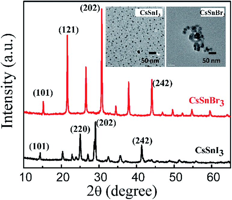 | ||
| Fig. 1 Powder XRD patterns of CsSnBr3 and CsSnI3 perovskite nanocrystals. The insets show the TEM images of CsSnBr3 and CsSnI3 perovskite nanocrystals. | ||
The UV-vis absorption and photoluminescence (PL) spectra of the CsSnBr3 and CsSnI3 nanocrystals were investigated, as shown in Fig. 2a and b. The insets in Fig. 2b are the photographs of CsSnBr3 and CsSnI3 nanocrystal suspensions under day light and UV light, respectively. The bandgaps of CsSnBr3 and CsSnI3 nanocrystals are roughly estimated to be 1.76 eV and 1.34 eV, respectively. By tuning the ratio of SnI2 and SnBr2 in the SnX2–TOP solution using during the facile hot injection method, CsSn(IxBr1−x)3 nanocrystals can also be prepared. The absorption and PL spectra are shown in Fig. S1 and S2,† respectively. The onset of absorption shifts to higher energy while replacing I− by Br−. Such a bandgap tuning property is similar to the previous reports in MASnX3, MAPbX3, CsSnX3, and CsPbX3 material systems.9,13,16,24–31 The PL spectra of the as-synthesized perovskite nanocrystals in solution showed an emission peak at 683 and 938 nm for CsSnBr3 and CsSnI3 nanocrystals, respectively.
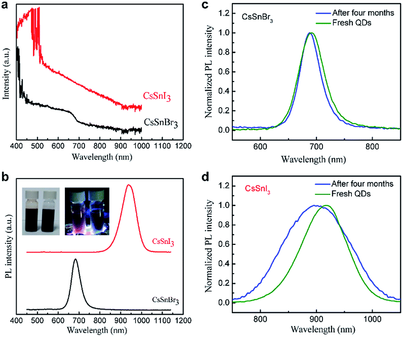 | ||
| Fig. 2 (a) Absorption and (b) PL spectra of CsSnBr3 and CsSnI3 perovskite nanocrystals. Insets in (b) show the CsSnBr3 and CsSnI3 nanocrystals in day light and under UV light. The PL spectra of the fresh and aged (c) CsSnBr3 and (d) CsSnI3 perovskite nanocrystals. | ||
The shelf stability of the CsSnBr3 and CsSnI3 nanocrystals in solution were also investigated, as shown in Fig. 2c and d. The CsSnBr3 and CsSnI3 nanocrystals suspensions were prepared and encapsulated in vials in the glove box. The vials were sealed and taken out of the glove box and stored in ambient condition for PL measurement. For CsSnBr3 QDs, when comparing the fresh and four months stored solution, the PL peak was shifted from 683 nm to 681 nm, FWHM was increased from 50 nm to 55 nm, and the PL peak intensity was decreased from to 44.12% after 4 months. For CsSnI3 QDs, the PL peak was shifted from 938 nm to 896 nm, FWHM was increased from 83 nm to 140 nm, and the PL peak intensity was decreased from to 15.26% after 4 months. The stability of CsSnBr3 QDs solution is better than CsSnI3 QDs solution (as shown in Fig. S3†). When the vial with CsSnI3 nanocrystals suspension was opened, there will be no PL signal after six hours. This is supposed to be related to the spontaneous oxidative conversion from CsSnI3 to Cs2SnI6.32
The steady-state PL spectra of CsSnBr3 and CsSnI3 nanocrystals in the temperature range between 80 K and 300 K are shown in Fig. 3a and b, respectively. With increasing the temperature, the PL peak shows a blue-shift tendency, the full width at half maximum (FWHM) of the PL spectra show a broadening characteristics, and the integrated PL intensity shows a continuous decrease. All these behaviors were also observed in MAPbI3, MAPbBr3, FAPbI3, FAPbBr3, CsPbBr3, CsPbI3, CsSnI3.4,33–36 The temperature-dependent PL is worthy to be investigated in detail since important physical parameters of perovskites such as exciton binding energy, charge carriers–phonon interaction and band gap can be estimated.
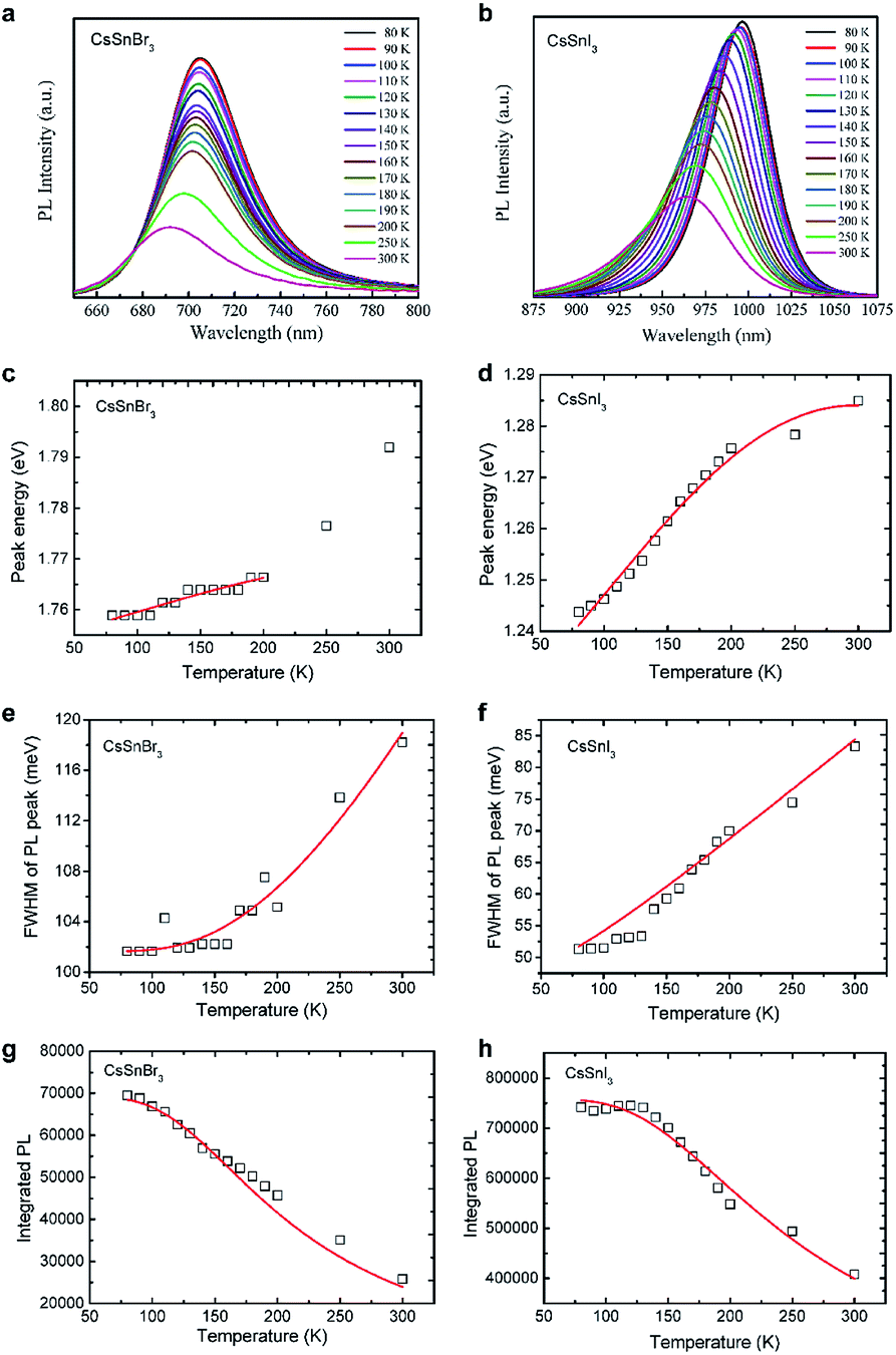 | ||
| Fig. 3 (a and b) Temperature-dependent PL spectra, (c and d) PL peak energy, (e and f) FWHM of the PL spectra, and (g and h) PL integrated intensity of (a, c, e and g) CsSnBr3 and (b, d, f and h) CsSnI3 perovskite nanocrystals. | ||
The peak energy of the PL of CsSnBr3 and CsSnI3 nanocrystals as a function of temperature is shown in Fig. 3c and d. The peak energy increases with increasing the temperature. Such a blue-shift in PL peak energy cannot be described by a traditional empirical relation, Eg = E0 − αT2/(T + β),37 which have been widely used to describe the temperature-dependent PL of conventional semiconductors. The empirical relation proposed by R. Pässler38 and an expression which follows the Bose–Einstein statistical factor39–41 are also not able to describe the blue-shift in PL peak energy.
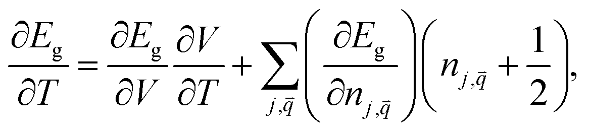
The dependence of the band gap at constant pressure comprises two contributions. One contribution is due to the thermal expansion of the lattice (changes in lattice constant), and another contribution is the renormalization of band energies by electron–phonon interactions.42–44 An expression was used to estimate the temperature-dependence of the band gap:33,34
 | (1) |
 is the occupation number of the phonon mode at j branch with wave vector
  . The first term in eqn (1) corresponds to the contribution of thermal expansion, while the second term is the contribution of electron–phonon interaction. Under the assumption of positive coefficient ∂Eg/∂V33 and one-oscillator mode,33,45 eqn (1) can be simplified as follow:33
| Eg(T) = E0 + ATET + AEP(2/(exp(ℏω/kT) − 1) + 1), | (2) |
As shown in Fig. 3e and f, the FWHM of the PL spectra broadens with increasing the temperature. The analysis on the temperature-dependent PL broadening is a widely used method to understand the electron–phonon coupling in inorganic semiconductors.5,33,35,36,47–49 Mechanisms related to the scattering between charge carriers and acoustic phonons, optical phonons or impurities have to be considered.36,48 The following relation has been proposed to describe the evolution of FWHM with temperature:
| Γ(T) = Γ0 + γacT + γLO/(eELO/kT − 1) + γimpe−Eb/kT, | (3) |
The evolution of integrated PL intensity is shown in Fig. 3g and h, which shows a continuous decrease with increasing the temperature. This behavior is an indication that thermal energy activates exciton dissociation or nonradiative relaxation process, which compete with radiative recombination. The temperature-dependent PL intensity can be fitted to the Arrhenius law:5,35,49–58
| I(T) = I0/(1 + Ae−Eb/(kT)), | (4) |
To demonstrate the capability of perovskite nanocrystals to be used in the real application, near-infrared light-emitting diodes based on CsSnI3 were realized. The device with a simple structure was adopted, that is ITO/PEDOT:PSS/emissive layer/LiF/Al. The emissive layer is a mixture composed of PVK, PBD, TPD, and CsSnI3 nanocrystals. The optical and electrical properties of the device based on CsSnI3 nanocrystals are shown in Fig. 4. The device with annealed emissive layer shown better performance than unannealed emissive layer. The maximum external quantum efficiently (EQE) of this device is about 0.007%. Such a low EQE value is attributed to the low quantum yield of the CsSnI3 nanocrystals9 and the leakage current. Considering the high electrical conductivity of CsSnI3,17 the leakage current may come from the percolation path in the emissive layer. Please note that there is no electroluminescence emission peak observed other than one belongs to the CsSnI3. Therefore, we suppose that the charge carriers are transported mainly through the percolation path constructed by CsSnI3 nanocrystals, and the electrons and holes are recombined on CsSnI3. To further increase the efficiency of the device by reducing the leakage current, an electron transport layer/hole blocking layer beneath the emissive layer and a hole transport layer/electron blocking layer above the emissive layer might be added.
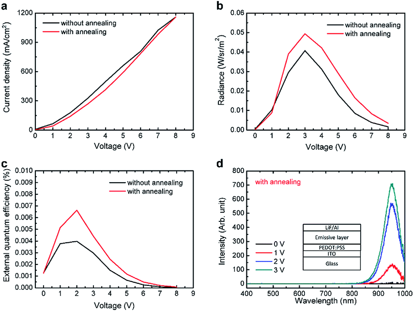 | ||
| Fig. 4 Optical and electrical properties of the LEDs based on CsSnI3. (a) Current density–voltage curves. (b) Radiance–voltage curves. (c) External quantum efficiency–voltage curves. (d) Electroluminescence spectra. | ||
In addition to use the perovskite nanocrystals in the emissive layer of the LED, we also use them to realize down-conversion color converter films. The color converter film was stacked on a blue LED (455 nm) for the down-conversion of blue light into the light with the wavelength of perovskite nanocrystals. The down-conversion color converter films were prepared by blending the CsSnBr3 or CsSnI3 nanocrystals with PMMA host polymer. Fig. 5 shows the PL spectra of the CsSnBr3/PMMA and CsSnI3/PMMA composite films. A commercial blue LED with 455 nm emission was used as the excitation source. The PL spectra show peak values at ∼455 nm from the blue LED and the secondary peaks at 673 and 931 nm for CsSnBr3/PMMA and CsSnI3/PMMA composite films, respectively. These peak positions are similar to the ones of pure perovskite nanocrystals. CsSn(BrxI1−x)3/PMMA composite films also works well for this demonstration, as shown in Fig S4.† These results demonstrated that a LED with emission wavelength range from 673 to 931 nm could be realized by stacking a down-conversion color converter film composed of CsSn(BrxI1−x)3 and PMMA on a LED.
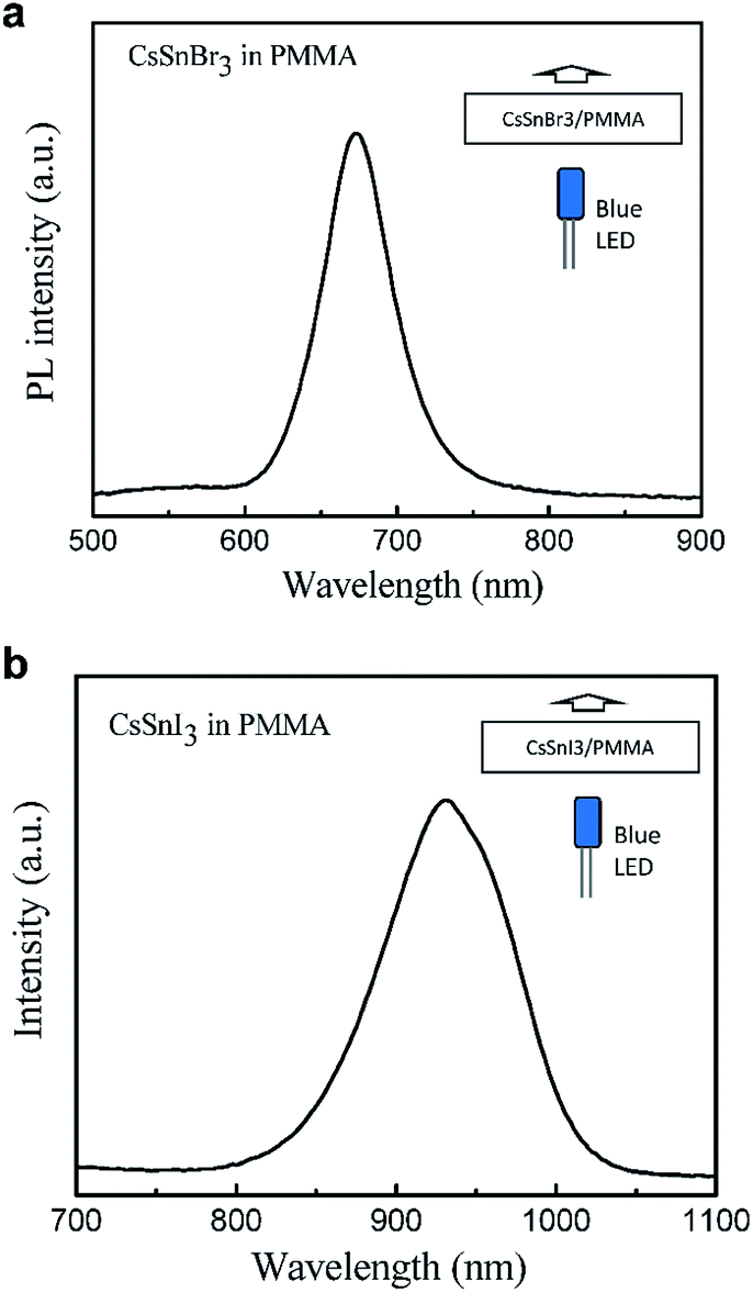 | ||
| Fig. 5 The characteristics of the color down-conversion films based on (a) CsSnBr3/PMMA and (b) CsSnI3/PMMA composite films. | ||
4. Conclusion
In summary, lead-free cesium tin halide CsSn(BrxI1−x)3 nanocrystals were synthesized by a facile hot injection method. The sizes of CsSnBr3 and CsSnI3 nanocrystals are 25 and 7 nm, respectively. Temperature-dependent PL is used to unveil their exciton binding energy, charge carriers–phonon interaction and band gap. Light-emitting diodes based on CsSnI3 and color down-conversion films based on CsSn(BrxI1−x)3 were demonstrated.Conflicts of interest
There are no conflicts to declare.Acknowledgements
This work was supported by the Ministry of Science and Technology (MOST) of Taiwan under grant numbers MOST 106-2112-M-003-016-MY3.References
- Z. Li, T. R. Klein, D. H. Kim, M. Yang, J. J. Berry, M. F. A. M. van Hest and K. Zhu, Nat. Rev. Mater., 2018, 3, 18017 CrossRef CAS.
- B. R. Sutherland and E. H. Sargent, Nat. Photonics, 2016, 10, 295 CrossRef CAS.
- M. Kangzhe, D. Xiang-Yun, Z. Ya-Wen and C. Su, J. Mater. Chem. C, 2017, 5, 9398 RSC.
- H. Zhu, Y. Fu, F. Meng, X. Wu, Z. Gong, Q. Ding, M. V. Gustafsson, M. T. Trinh, S. Jin and X. Y. Zhu, Nat. Mater., 2015, 14, 636 CrossRef CAS.
- X. Li, Y. Wu, S. Zhang, B. Cai, Y. Gu, J. Song and H. Zeng, Adv. Funct. Mater., 2016, 26, 2435 CrossRef CAS.
- C. Yang, Y. Wu, Q. Ma and W. H. Zhang, J. Energy Chem., 2018, 27, 622–636 CrossRef.
- X. He, Y. Qiu and S. Yang, Adv. Mater., 2017, 29, 1700775 CrossRef.
- F. Liu, Y. Zhang, C. Ding, S. Kobayashi, T. Izuishi, N. Nakazawa, T. Toyoda, T. Ohta, S. Hayase, T. Minemoto, K. Yoshino, S. Dai and Q. Shen, ACS Nano, 2017, 11, 10373–10383 CrossRef CAS.
- T. C. Jellicoe, J. M. Richter, H. F. J. Glass, M. Tabachnyk, R. Brady, S. E. Dutton, A. Rao, R. H. Friend, D. Credgington, N. C. Greenham and M. L. Böhm, J. Am. Chem. Soc., 2016, 138, 2941 CrossRef CAS.
- A. Wang, Y. Guo, F. Muhammad and Z. Deng, Chem. Mater., 2017, 29, 6493–6501 CrossRef CAS.
- A. B. Wong, Y. Bekenstein, J. Kang, C. S. Kley, D. Kim, N. A. Gibson, D. Zhang, Y. Yu, S. R. Leone, L. W. Wang, A. P. Alivisatos and P. Yang, Nano Lett., 2018, 18, 2060–2066 CrossRef CAS.
- F. Liu, C. Ding, Y. Zhang, T. S. Ripolles, T. Kamisaka, T. Toyoda, S. Hayase, T. Minemoto, K. Yoshino, S. Dai, M. Yanagida, H. Noguchi and Q. Shen, J. Am. Chem. Soc., 2017, 139, 16708–16719 CrossRef CAS.
- L. J. Chen, C. R. Lee, Y. J. Chuang, Z. H. Wu and C. Chen, J. Phys. Chem. Lett., 2016, 7, 5028 CrossRef CAS.
- I. Chung, B. Lee, J. He, R. P. H. Chang and M. G. Kanatzidis, Nature, 2012, 485, 486 CrossRef CAS.
- M. H. Kumar, S. Dharani, W. L. Leong, P. P. Boix, R. R. Prabhakar, T. Baikie, C. Shi, H. Ding, R. Ramesh, M. Asta, M. Graetzel, S. G. Mhaisalkar and N. Mathews, Adv. Mater., 2014, 26, 7122 CrossRef CAS.
- D. Sabba, H. K. Mulmudi, R. R. Prabhakar, T. Krishnamoorthy, T. Baikie, P. P. Boix, S. Mhaisalkar and N. Mathews, J. Phys. Chem. C, 2015, 119, 1763 CrossRef CAS.
- J. Zhang, C. Yu, L. Wang, Y. Li, Y. Ren and K. Shum, Sci. Rep., 2014, 4, 6954 CrossRef CAS.
- W. L. Hong, Y. C. Huang, C. Y. Chang, Z. C. Zhang, H. R. Tsai, N. Y. Chang and Y. C. Chao, Adv. Mater., 2016, 28, 8029 CrossRef CAS.
- K. Sasha and B. Yehonadav, Nanoscale, 2019, 11, 8665 RSC.
- V. Alessandro, P. Maddalena, B. Daniele, C. Carlo, Q. Paolo and M. Lorenzo, Front. Chem., 2020, 8, 35 CrossRef.
- Y. Chonglong, C. Zhuo, J. W. Jian, P. William, V. Nemanja, T. K. John and S. Kai, J. Appl. Phys., 2011, 110, 063526 CrossRef.
- H.-C. C. Oscar, Q. Tian, S. Matthew and H. S. Dong, Nanoscale, 2020, 12, 13113 RSC.
- I. Chung, J. H. Song, J. Im, J. Androulakis, C. D. Malliakas, H. Li, A. J. Freeman, J. T. Kenney and M. G. Kanatzidis, J. Am. Chem. Soc., 2012, 134, 8579 CrossRef CAS.
- F. Hao, C. C. Stoumpos, D. H. Cao, R. P. H. Chang and M. G. Kanatzidis, Nat. Photonics, 2014, 8, 489 CrossRef CAS.
- N. K. Kumawat, A. Dey, A. Kumar, S. P. Gopinathan, K. L. Narasimhan and D. Kabra, ACS Appl. Mater. Interfaces, 2015, 7, 13119 CrossRef CAS.
- J. H. Noh, S. H. Im, J. H. Heo, T. N. Mandal and S. I. Seok, Nano Lett., 2013, 13, 1764 CrossRef CAS.
- B. Suarez, V. Gonzalez-Pedro, T. S. Ripolles, R. S. Sanchez, L. Otero and I. Mora-Sero, J. Phys. Chem. Lett., 2014, 5, 1628 CrossRef CAS.
- S. A. Kulkarni, T. Baikie, P. P. Boix, N. Yantara, N. Mathews and S. Mhaisalkar, J. Mater. Chem. A, 2014, 2, 9221 RSC.
- G. Nedelcu, L. Protesescu, S. Yakunin, M. I. Bodnarchuk, M. J. Grotevent and M. V. Kovalenko, Nano Lett., 2015, 15, 5635 CrossRef CAS.
- L. Protesescu, S. Yakunin, M. I. Bodnarchuk, F. Krieg, R. Caputo, C. H. Hendon, R. X. Yang, A. Walsh and M. V. Kovalenko, Nano Lett., 2015, 15, 3692 CrossRef CAS.
- Q. A. Akkerman, V. D'Innocenzo, S. Accornero, A. Scarpellini, A. Petrozza, M. Prato and L. Manna, J. Am. Chem. Soc., 2015, 137, 10276 CrossRef CAS.
- X. Qiu, B. Cao, S. Yuan, X. Chen, Z. Qiu, Y. Jiang, Q. Ye, H. Wang, H. Zeng, J. Liu and M. G. Kanatzidis, Sol. Energy Mater. Sol. Cells, 2017, 159, 227 CrossRef CAS.
- K. Wei, Z. Xu, R. Chen, X. Zheng, X. Cheng and T. Jiang, Opt. Lett., 2016, 41, 3821 CrossRef CAS.
- C. Yu, Z. Chen, J. J. Wang, W. Pfenninger, N. Vockic, J. T. Kenney and K. Shum, J. Appl. Phys., 2011, 110, 063526 CrossRef.
- H. Diab, G. Trippé-Allard, F. Lédée, K. Jemli, C. Vilar, G. Bouchez, V. L. R. Jacques, A. Tejeda, J. Even, J. S. Lauret, E. Deleporte and D. Garrot, J. Phys. Chem. Lett., 2016, 7, 5093 CrossRef CAS.
- A. D. Wright, C. Verdi, R. L. Milot, G. E. Eperon, M. A. Pérez-Osorio, H. J. Snaith, F. Giustino, M. B. Johnston and L. M. Herz, Nat. Commun., 2016, 7, 11755 CrossRef.
- Y. Varshni, Physica, 1967, 34, 149 CrossRef CAS.
- R. Pässler, Phys. Status Solidi B, 1997, 200, 155 CrossRef.
- L. Viña, S. Logothetidis and M. Cardona, Phys. Rev. B: Condens. Matter Mater. Phys., 1984, 30, 1979 CrossRef.
- S. Logothetidis, L. Via and M. Cardona, Phys. Rev. B: Condens. Matter Mater. Phys., 1985, 31, 947 CrossRef CAS.
- P. Lautenschlager, M. Garriga, S. Logothetidis and M. Cardona, Phys. Rev. B: Condens. Matter Mater. Phys., 1987, 35, 9174 CrossRef CAS.
- P. B. Allen and M. Cardona, Phys. Rev. B: Condens. Matter Mater. Phys., 1983, 27, 4760 CrossRef CAS.
- P. Lautenschlager, P. B. Allen and M. Cardona, Phys. Rev. B: Condens. Matter Mater. Phys., 1985, 31, 2163 CrossRef CAS.
- A. Göbel, T. Ruf, M. Cardona, C. T. Lin, J. Wrzesinski, M. Steube, K. Reimann, J. C. Merle and M. Joucla, Phys. Rev. B: Condens. Matter Mater. Phys., 1998, 57, 15183 CrossRef.
- J. Bhosale, A. K. Ramdas, A. Burger, A. Muñoz, A. H. Romero, M. Cardona, R. Lauck and R. K. Kremer, Phys. Rev. B: Condens. Matter Mater. Phys., 2012, 86, 195208 CrossRef.
- L. Huang and W. R. L. Lambrecht, Phys. Rev. B: Condens. Matter Mater. Phys., 2013, 88, 165203 CrossRef.
- S. Rudin, T. L. Reinecke and B. Segall, Phys. Rev. B: Condens. Matter Mater. Phys., 1990, 42, 11218 CrossRef CAS.
- J. Lee, E. S. Koteles and M. O. Vassell, Phys. Rev. B: Condens. Matter Mater. Phys., 1986, 33, 5512 CrossRef CAS.
- Z. F. Shi, X. G. Sun, D. Wu, T. T. Xu, Y. T. Tian, Y. T. Zhang, X. J. Li and G. T. Du, J. Mater. Chem. C, 2016, 4, 8373 RSC.
- K. Wu, A. Bera, C. Ma, Y. Du, Y. Yang, L. Li and T. Wu, Phys. Chem. Chem. Phys., 2014, 16, 22476 RSC.
- S. Sun, T. Salim, N. Mathews, M. Duchamp, C. Boothroyd, G. Xing, T. C. Sum and Y. M. Lam, Energy Environ. Sci., 2014, 7, 399 RSC.
- T. J. Savenije, C. S. Ponseca Jr, L. Kunneman, M. Abdellah, K. Zheng, Y. Tian, Q. Zhu, S. E. Canton, I. G. Scheblykin, T. Pullerits, A. Yartsev and V. Sundström, J. Phys. Chem. Lett., 2014, 5, 2189 CrossRef CAS.
- S. M. Lee, C. J. Moon, H. Lim, Y. Lee, M. Y. Choi and J. Bang, J. Phys. Chem. C, 2017, 121, 26054 CrossRef CAS.
- A. Yangui, S. Pillet, A. Mlayah, A. Lusson, G. Bouchez, S. Triki, Y. Abid and K. Boukheddaden, J. Chem. Phys., 2015, 143, 224201 CrossRef CAS.
- J. Fujisawa and T. Ishihara, Phys. Rev. B: Condens. Matter Mater. Phys., 2004, 70, 205330 CrossRef.
- D. S. Jiang, H. Jung and K. Ploog, J. Appl. Phys., 1988, 64, 1371 CrossRef CAS.
- X. Hong, T. Ishihara and A. V. Nurmikko, Phys. Rev. B: Condens. Matter Mater. Phys., 1992, 45, 6961 CrossRef CAS.
- T. Ishihara, J. Takahashi and T. Goto, Phys. Rev. B: Condens. Matter Mater. Phys., 1990, 42, 11099 CrossRef CAS.
Footnotes |
| † Electronic supplementary information (ESI) available. See DOI: 10.1039/d0ra06139e |
| ‡ K. P. O. Mahesh and Che-Yu Chang contributed equally to this work. |
| This journal is © The Royal Society of Chemistry 2020 |