
 Open Access Article
 This Open Access Article is licensed under a Creative Commons Attribution-Non Commercial 3.0 Unported Licence
Microstructure and long-term stability of solder joints on nickel-plated aluminium formed during short soldering times
Angela De Rose *ab,
Gabriele Mikolascha,
Mathias Kampa,
Achim Krafta and
Mathias Nowottnickb
*ab,
Gabriele Mikolascha,
Mathias Kampa,
Achim Krafta and
Mathias Nowottnickb
aFraunhofer Institute for Solar Energy Systems ISE, Heidenhofstraße 2, 79110 Freiburg, Germany. E-mail: angela.de.rose@ise.fraunhofer.de
bInstitute of Electronic Appliances and Circuits, Faculty of Computer Science and Electrical Engineering, University of Rostock, Albert-Einstein-Straße 2, 18059 Rostock, Germany
First published on 4th November 2020
Abstract
Within this work, we demonstrate that an easy soldering process in combination with wet chemical coating is suitable to realize a strong and reliable solder interconnection of Al substrates, even at short soldering times <5 s in ambient air. The microstructure of solder joints on wet chemically treated aluminum foils is investigated. A single and double zincate pre-treatment are compared to activate the Al surface, followed by electroless Ni plating. The quality of the solderable Ni surface is characterized by contact angle measurements, yielding good wettability (<60°), which is also achieved after isothermally heating (250 °C) the Ni-coated Al foils for 100 min. The microstructure of the Sn62Pb36Ag2 solder joints is investigated by SEM and EDX of cross sections, directly after soldering as well as after isothermal aging at 85 °C. Under the used soldering conditions, with a soldering temperature at about 280 °C, diffusion zones <500 nm were identified. Nonetheless, high peel forces after soldering >5 N mm−1 show stable values under aging conditions of 85 °C for 1000 hours. This could be correlated to a mixed fracture pattern, promoting the high adhesion due to the absence of a dominant failure mechanism.
Introduction
It is well known that aluminium (Al) has a lot of diverse advantages and is therefore widely used for engineering applications.1 It would go beyond the scope of this article to mention all of them, but the most prominent will be addressed in the following.The possibility of creating a variety of Al alloys makes it suitable for a wide range of applications. It has an outstanding strength-to-weight ratio (lightweight yet still extremely strong), which is advantageous for aerospace and modern buildings, i.e. skyscrapers. Its high formability allows Al to be used for nearly every conceivable shape, e.g. for architectural structures. In electrical engineering, many electronic components (capacitors, antennae, radar) are made of Al due to its high electrical and thermal conductivity. For marine applications, the high resistance of Al to corrosion is utilized to withstand many different environmental settings, requiring a minimum of maintenance due to a long lifespan. Although the recyclability of Al is comparably high,2 the demand for Al and the recirculated quantity of Al is still increasing worldwide, e.g. in power lines, rolled products, refrigerators, air conditioning, solar modules, automotive industry, heat sinks for cooling in microelectronics, etc.1,3
A major challenge of Al is the formation of solder joints. It is well known that Al forms a thin native oxide film as soon as it is exposed to air.4 Besides other joining technologies as vacuum brazing,5,6 inert gas welding,7 ultrasonic welding8 or laser welding,9 one possibility is to coat the bare Al surface to enable a solder connection. Several easy and industrially feasible coating methods are known, which are reviewed in one of our previous publications.10 Solderable Al surfaces extend the usage of Al components, especially for applications in a lower temperature range.
In this work, we investigate a wet chemical coating by zincate treatment and electroless nickel plating to allow solder joint formation within very short (<5 s) soldering times.
A pre-treatment of Al surfaces with zincate has been reported in literature11,12 and was first patented in 1927 by Hewitson et al.,13 to the best of the author's knowledge. A key attractiveness is the simple and low cost process14 and the possibility to use batch and inline processes. Other research investigated the influence of the number of cycles of the Zn process (w/o, single, double or even triple)15,16 as well as the variation of the NaOH content17 on the deposited metal layers. Several studies include surface analysis (of Zn and Ni), adhesion issues and analysis of failure modes. In addition, zincate treatment is examined in combination with sputtered Al films15 or Al sheets.16,18,19
The fundamental approach of this process sequence can be illustrated by the standard electrode potential E0. In Fig. 1, this quantity is correlated with the measured static contact angle α of a Sn60Pb40 solder droplet on different surfaces. On a 200 μm thick Al foil, a high contact angle of αAl = (141.7 ± 4.3)° is measured (magenta in Fig. 1). When such a foil is coated with a double Zn process, as explored in this work, the measured contact angle decreases to αZn = (117.0 ± 15.1)° (grey). After subsequent Ni plating, the angle could be reduced to αNi = (27.7 ± 2.9)° (cyan). A small contact angle implies good wettability, which is the main requirement for solder joint formation. From a technical point of view, α < 90° leads to wetting, so that 117° for Zn is not satisfactory.
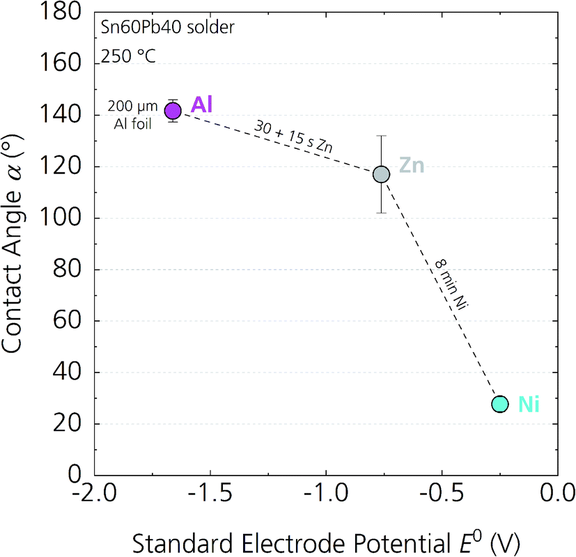 | ||
| Fig. 1 Dependence of the contact angle α of liquid solder (Sn60Pb40) on pure Al foil (magenta), Zn coated Al foil (grey) and Ni coated Al foil (cyan) of the standard electrode potential E0. The wet chemical coating steps represent the sequence of coating used in this work. | ||
The bare Al has a negative E0Al = −1.662 V, when measured under standard conditions (298 K, 100 kPa, 1.0 mol dm−3) with respect to the standard hydrogen electrode.20 Fundamentally, coating of Al with less reactive metals changes |E0| to higher values.20 This is the case for zinc (Zn). When deposited out of an alkaline solution, this can remove the problematic native Al2O3 layer. With E0Zn = −0.762 V, Zn is less reactive to oxygen then Al, but reactive enough to build a ZnO layer, which also impedes wetting by solder. Nevertheless, the Zn clusters on top of the Al surface prevent reoxidation of the Al underneath and serve as nuclei for subsequent electroless Ni plating. The Ni surface has a standard electrode potential of E0Ni = −0.250 V, closer to those of Sn (E0Sn = −0.138 V), Cu (E0Cu = 0.521 V) and Ag (E0Ag = 0.7996 V).20 On these more noble surfaces wetting with liquid solder is excellent, which enables reliable soldering processes. The relevant microstructure of the surface modifications and subsequently employed solder joints are investigated in this work. We focus on solder joints, formed within less than 5 s soldering time (contact soldering), to evaluate suitability for applications with a high throughput.
Experimental
Aluminium foil
Rolled Al foil with a thickness of 200 μm from monolithic Al sheets (alloy 1200, 99%wt Al, annealed) of Hydro Aluminium Rolled Products GmbH is used.3 The foil is cut to (80 × 160) mm2 and multiple identical samples are processed for each variation.Coating of the aluminium foils can be separated into two main process steps: zincate treatment and nickel plating. Both processes are carried out on lab scale equipment at Fraunhofer ISE and are described in the following.
Zincate process
The zincate solution is used to remove the native Al2O3 layer and to activate the aluminium surface. We test single zincate (s-Zn) as well as double zincate (d-Zn) processes to prepare the Al foils before Ni plating. This process is widely known as pre-treatment for Al coatings or surface modification.17–19A commercially available Zn bath of SurTec® 652Q based on NaOH and ZnSO4 with pH = 14 is used at room temperature (RT). The ingredients of the bath are listed in Table 2.
This alkaline NaOH based solution reacts with the Al2O3 surface layer and leads to dissolution in the bath:21
| 2NaOH + Al2O3 + 3H2O → 2NaAl(OH)4 | (1) |
The underlying Al can then react with the Zn leading to Zn deposition in the form of small seeds. This displacement reaction during Zn treatment is described by:
| 3Na2Zn(OH)4 + 2Al → 2NaAl(OH)4 + 4NaOH + 3Zn | (2) |
Zn is reduced and Al is oxidized in this reaction. Electrons, released by the anodic reaction, are used within the cathodic reaction resulting in Zn deposition. Within this work, the process time for the s-Zn treatment is kept constant at 30 s bath time. For the d-Zn treatment, we dipped the samples into nitric acid (30%) after the first Zn step, to remove the deposited Zn layer and to clean the Al:
| Zn + 2HNO3 + 6H2O → Zn(NO3)2·6H2O + H2 | (3) |
A second Zn step leads to improved homogeneity of the Zn layer, with more seeds on top of the Al as shown in the results. Table 1 summarises the process variations for Zn treatment and Ni plating applied in this work. A variation of the second zincate treatment between 15 s and 30 s does not yield significant differences for the parameters tested in this work, and will be collectively referred to as d-Zn.
| Zincate treatment | Electroless plating | ||
|---|---|---|---|
| Single (s-Zn) | Double (d-Zn) | Ni | |
| Process time | 30 s | 30 s + (15–30) s | 8 min |
| Bath temperature | RT | RT | 88 °C |
| pH | 14 | 14 | 4.8 |
| Amount (%) | Ingredient | |
|---|---|---|
| 10–20 | Sodium hydroxide | NaOH |
| 5–10 | Zinc sulfate heptahydrate | ZnSO4·7H2O |
| 3–7 | Nickel(II) sulfate hexahydrate | NiSO4·6H2O |
| <1 | Copper(II) sulfate pentahydrate | CuSO4·5H2O |
Nickel plating
In contrast to electroplating, no external electric current or voltage and no sacrificial Ni anode is required for electroless plating. This allows the formation of dense and homogeneous Ni coatings by the deposition of Ni, chemically available in the solution (reducing agent). We have used a commercially available Ni electrolyte ELV 808 of MacDermid GmbH based on Ni sulfate with a low sodium hypophosphite content of about 30 g l−1 and pH ≈ 4.8. The bath is constantly stirred and the temperature is set to (88 ± 2) °C resulting in a deposition rate of about 18 μm h−1 during electroless plating:21| Ni2+ + H2PO2− + H2O → Ni + H2PO3− + 2H+ | (4) |
Hydrated sodium hypophosphite reacts as reducing agent with the Ni ions of the electrolyte.
For our study, we kept the plating time constant at 8 min, leading to a Ni layer of about 2.0–2.5 μm thickness.
Soldering
The soldering process is carried out with a solder iron at a soldering temperature of Ts = (285 ± 15) °C. To support the heat flow of the iron into the solder joint, the samples are placed on a hotplate with THP = (120 ± 5) °C.Cu ribbons with a cross section of 0.2 × 1.5 mm2 and length of (160 ± 5) mm are soldered onto the coated Al foils. They are coated with a layer of Sn62Pb36Ag2 (Tliq = 179 °C) of about (15 ± 5) μm thickness to realize a solder connection between coating and Cu core of the ribbon. For oxide removal, a no-clean organic flux based on adipic acid is used.
The evaluated coatings are optimized to allow for a solder formation within very short soldering times. This enables a high throughput in production lines as it is required in soldering of silicon solar cells in industry.22 In our experiments, we used short soldering times, estimated to be ts < 5 s, as far as manual soldering allows. Therefore, eutectic or even near-eutectic solder alloys are used for the interconnection. Subject to the regulations in Art. 2(4)(i) in 2011/65/EU (RoHS),23 the usage of Pb in photovoltaics is excluded, whereas Sn62Pb36Ag2 or the cheaper alternative Sn60Pb40 (Tliq = 183 °C) are used.
Metallography
For microstructural analysis of the solder joints, cross section samples are prepared by metallography. After soldering the ribbons onto the 200 μm thick Al foil, small pieces of (1 × 1) cm2 are cut out and embedded into graphite-containing epoxy.24 After grounding the sample, the interface of interest is polished and the quality of the cross section is checked by optical microscopy before further analysis with scanning electron microscopy.Analysis and characterisation
Before soldering, the quality of the coating is characterised by contact angle measurements to evaluate the wettability. A device of the OCA series of DataPhysics is used, which is extended by a hotplate to heat up the samples above the liquidus temperature of the solder alloy. To determine the static contact angle, the sessile drop method25 is applied by fitting a tangent line at the contact point along the droplet profile. The droplet profile itself is reproduced by an elliptical fit within the contrast image after full liquidation of the solder droplet.Each coating is characterised by 10 measurements on individual samples. For each measurement, (11 ± 1) mg of Sn60Pb40 are placed onto the fluxed coating, whereafter the mean of left and right contact angle is determined. Good wettability is given for a contact angle α < 60°, excellent wetting for α < 30°.25,26
Within this work, Sn62Pb36Ag2 solder is used to compare our results to older work. Only for contact angle measurements, we applied Sn60Pb40 as it is meanwhile the most commonly used solder alloy in PV. It known, that both alloys perform very similar, whereas additional Ag within the solder slightly improves wettability. Therefore, the results obtained in this work for Sn60Pb40 indicate an upper limit (slightly higher contact angle) of the Sn62Pb36Ag2 alloy.
For topography scans, a confocal microscope (μsurf solar) of NanoFocus AG is used. An area of (0.8 × 0.8) mm2 of the sample surface is scanned with a monochromatic LED light source with a wavelength of 505 nm and an objective with 20× magnification, NA = 0.6 and a z-resolution of Δz = 4 nm.
To extract height profiles, the mean of 21 line scans along 33 μm is calculated and levelled to the sample substrate.
For mechanical characterisation, peel tests according to DIN EN 50461 (ref. 27) are performed on a zwicki Z0.5 TN peel testing machine of Zwick Roell. After soldering, one end of the ribbon is mounted into a clamp and peeled off with 50 mm min−1 under an angle of 90° to the sample surface. To take inhomogeneities both of the coating and the solder joints into account, each test is carried out for a length of 150 mm and repeated with at least five samples. The peel force F is measured along the position x of the measurement length. The width w = 1.5 mm of the soldered ribbons is used to normalize the recorded force values Fi per position to a defined contact width of the joint.
After testing, the fracture pattern is inspected by scanning electron microscopy in top view or tilted images.
Scanning electron microscopy (SEM) is done on the Auriga 60 setup of Carl Zeiss Microscopy on a crossbeam workstation, using a secondary electron detector. To get information on the involved material combinations, energy dispersive X-ray spectroscopy (EDX) is carried out with a Bruker Quantax XFlash 6|60 detector.
Isothermal aging of the solder joints is done within an oven in ambient air. The temperature is kept constant at (85 ± 5) °C.
Results and discussion
Surface characterisation after coating
To provide a solderable coating on top of the Al foil, we used a wet chemical process to deposit Zn either within a single (s-Zn) or double zincate (d-Zn) process (cf. Experimental section). SEM top view images at 800× magnification serve for process control after each step (Fig. 2). The images are compared by a particle detection algorithm, identifying Zn seeds of different particle size aZn. The minimum particle size is set to 0.2 μm2, for shapes with a circularity of 0.3–1.0. These arbitrary thresholds limit the influence of the blurry background and emphasizes clearly identifiable particles. This quantitative evaluation will to some extend underestimate the Zn coverage and only serves for comparison between s-Zn and d-Zn. The amount of deposited Zn seeds ζ is quantified by the total area of detected Zn seeds AZn within the SEM image section ASEM (57.7 μm × 43.1 μm). The evaluated data is given in Table 3. | ||
| Fig. 2 SEM top view images of (a) 200 μm thick roll milled Al foil. The coating quality is proven by SEM showing the Zn deposition after 30 s s-Zn in (b) and double Zn treatment 30 s + 15 s in (d). The resulting Ni layer after 8 min electroless plating is given in (c and e), respectively. All images taken at a magnification of 800× with 10 kV. | ||
| s-Zn (30 s) | d-Zn (30 s + 15 s) | |
|---|---|---|
| Zn coverage ζ (%) | 4.0 ± 1.0 | 10.8 ± 2.0 |
| Mean Zn particle size aZn (μm2) | 0.44 ± 0.05 | 0.41 ± 0.05 |
After 30 s of dipping the 200 μm thick milled Al foil (Fig. 2a) into the alkaline Zn bath, about ζs-Zn = (4.0 ± 1.0)% of the Al foil is covered with Zn seeds with a mean particle size of as-Zn = (0.44 ± 0.05) μm2 (Fig. 2b). Subsequent electroless Ni plating leads the Zn to dissolve in the bath, whereas a Ni layer is formed in direct contact with the Al surface. After 8 min of plating, a closed Ni layer of about 2 μm thickness is formed (Fig. 2c), which yields a lumpy surface, typical for plated Ni surfaces.12 A double zincate process (30 s + 15 s, Fig. 2d) results in a more homogeneous Ni layer (Fig. 2e). Due to a larger Zn coverage of ζd-Zn = (10.8 ± 2.0)%, the resulting Ni layer is smoother since more Zn seeds are starting points for Ni growth. It is interesting to point out that the mean Zn particle size stays the same (ad-Zn = (0.41 ± 0.05) μm2).
For the reliable formation of a solder joint on a metal surface, a good surface wettability with liquid solder is an important requirement. The static contact angle α between the substrate, liquid Sn60Pb40 solder and air is measured on a hotplate at (250 ± 5) °C.
Fig. 3a shows the results of the contact angle measurements for Al foil coated with pure Zn, for the Ni surface after s-Zn and Ni plating and for d-Zn and Ni plating. The evaluated d-Zn process (w/o Ni) is optimized to result in a closed Zn surface. Wetting of liquid Sn60Pb40 on pure Zn is poor (αZn = (117.0 ± 15.1)°), as it is expected from the electrochemical potential E0Zn = −0.762 V (cf. Fig. 1). The used no-clean flux is not able to remove all native oxides of the Zn surface. Both Ni-coated Al foils show excellent wetting. Despite the different surface morphology of the Ni surfaces (Fig. 2c and e), the contact angle is measured to be similar with αs-Zn+Ni = (27.7 ± 9.2)° and αd-Zn+Ni = (32.6 ± 4.3)°.
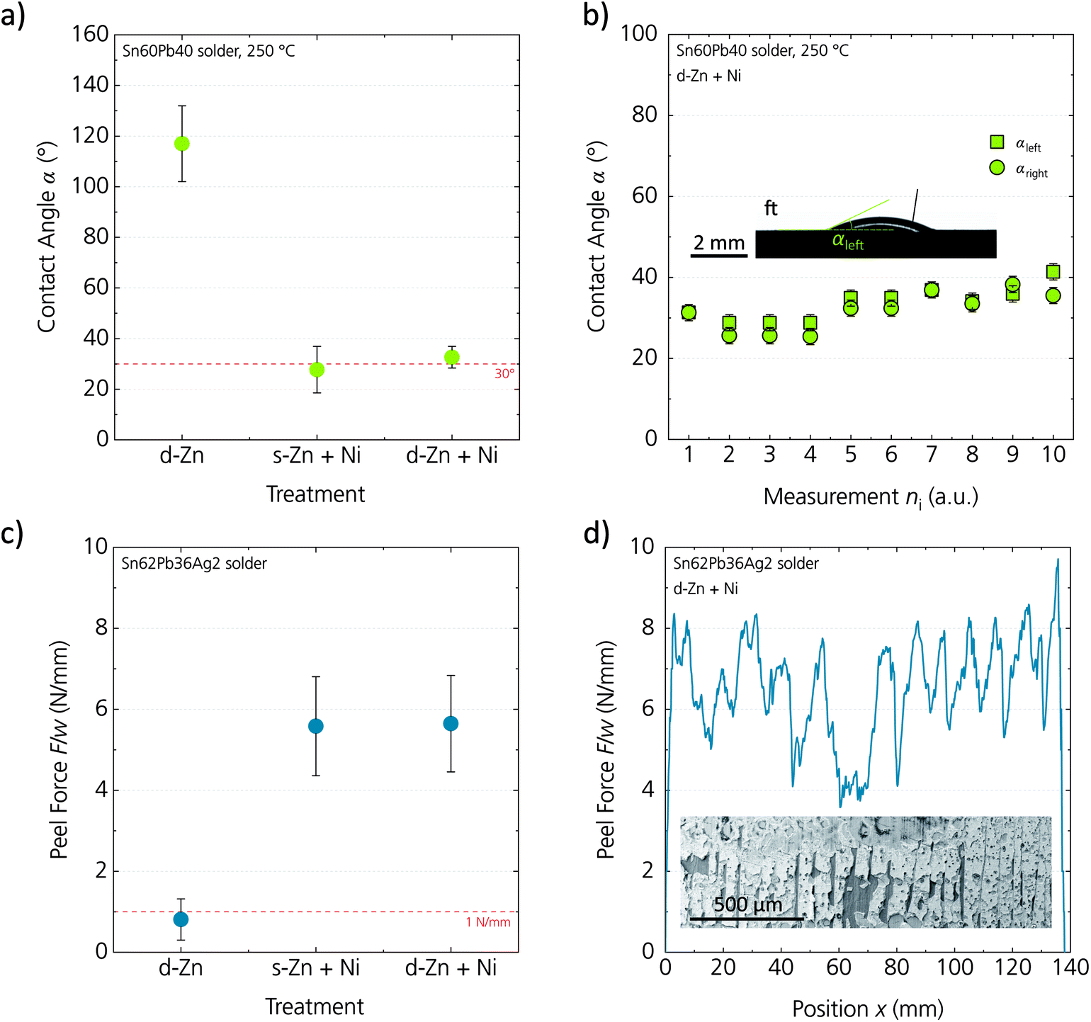 | ||
| Fig. 3 (a) Contact angle for three different treatments. (b) Details of measurements on d-Zn + Ni with example for contrast image of liquid solder droplet. (c) Adhesion for three different treatments. (d) Detail of measurements on d-Zn + Ni with a part of the fracture pattern after the peel test (SEM image, 20 kV). | ||
For the evaluation of the mean contact angle given in Fig. 3a, each surface is measured 10 times. The standard deviation is given by the error bars. For good wettable surfaces, a circular or elliptical fit is used for evaluating the shape of the droplet in the contrast image (see inset in Fig. 3b). The systematic error is given by the error bars in Fig. 3b. The elliptical fit considers asymmetric droplets and results in a difference between left and right contact angle. For the tested Al foils, the standard deviation is very small, indicating a homogeneously coated Al foil.
Mechanical characterization of solder joints
After s-Zn and d-Zn treatment and subsequent Ni plating, both surfaces allow for contact formation by soldering. The mechanical stability of the solder joints is characterised by a 90° peel test. The results for the differently treated Al surfaces are given in Fig. 3c. As expected, a good adhesion (high peel force F/w) is given for good wettable surfaces indicated by a small contact angle α in Fig. 3a. For an application on the rear side of a solar cell, the joints have to withstand the string handling after soldering. The measured peel forces for the Ni coated foils are much higher than the required value of 1 N mm−1, given in the standard DIN EN 50461.27 Fig. 3d presents data of a peel test on a d-Zn + Ni treated Al foil. Although the force is fluctuating, all values stay above 4 N mm−1. A small section of the fracture pattern after the peel test is given by a top view SEM image in the inset. We observe diverse fracture patterns, to fail, which is an ideal condition for measuring high adhesion of solder joints. The details of the fracture mechanism are discussed later.From those results, we conclude that both processes, s-Zn + Ni and d-Zn + Ni, are suitable to provide a solderable coating on Al which allows contact formation by SnPb-solders. Due to the very high adhesion, the process times for Zn and Ni may be further reduced, while maintaining a well adherent solder joint. This optimization was not focus of this contribution and could be addressed in future work.
Microstructure of solder joints
For comparison, metallographic cross sections are prepared of a solder joint on s-Zn + Ni and d-Zn + Ni coated Al foils, respectively. Fig. 4 shows SEM images with corresponding EDX mappings. In Fig. 4a, a solder joint on s-Zn + Ni coated Al with Sn62Pb36Ag2 solder is presented, taken at 2400× magnification and 20 kV. A solder joint on d-Zn + Ni coated Al is given in Fig. 4b, taken at a magnification of 1200×. In the presented examples, the solder layer in (b) is even twice as thick as in (a): (43.3 ± 0.6) μm compared to (21.2 ± 0.9) μm. This is not an effect of our variation and just a coincidence; at different positions along the solder joint, the thickness of the solder layer can vary significantly, e.g. due to holding down clamps. Our investigations show that this difference does not affect the performance of the solder joints characterised in this study. All joints are crack- and void-free and very homogeneous over the width of the ribbon w = 1.5 mm. | ||
| Fig. 4 SEM cross section images taken at 20 kV of solder joints (SnPbAg) on Al foil coated with (a) s-Zn + Ni and (b) d-Zn + Ni. The corresponding EDX mappings show the element distribution. Note the different scales of the SEM images. | ||
The comparison of those two images illustrates the different surface morphology of the Ni layer for both processes, similar to the finding from the top view images in Fig. 2c and e. We analysed five cross sections each along the soldered ribbon, covering about 150 mm of coating, tested on several Al foils. For all foils treated with s-Zn + Ni, the resulting Ni layer is rougher, depending on the process time of the Zn treatment.
Our results show comparable performance of solder joints on Ni coated Al foils, either treated with s-Zn or d-Zn. In the following, we focus on solder joints on d-Zn + Ni coated Al, investigating their long-term stability under aging conditions.
Isothermal aging of solder joints
For a long lifetime and a possible outdoor application, the surfaces to be soldered (here the coating) and the solder joints have to fulfil certain reliability requirements:28• Stability of coating regarding oxidation
• No degradation of solder joints to not increase the series resistance or reduce the mechanical stability
• Minimized brittle phase formation within the solder joints.
After coating, the Al surface may re-oxidize if the time between coating and soldering is too long. Additionally, the surface quality may change during the soldering process at elevated temperature. To analyse this, we did in situ contact angle measurements at 250 °C, a typical soldering temperature for SnPb-based solder alloys.
In Fig. 5, the change of the contact angle αi/α0 is plotted against the time t of six identical samples placed on a hotplate heated up to 250 °C. Each value αi is normalized to the initial value α0 of the unaged sample at t = 0. For each sample 1–6, a different solder droplet with mSnPb = (11 ± 1) mg is used. We tested a coated Al foil, treated with a d-Zn and Ni plating.
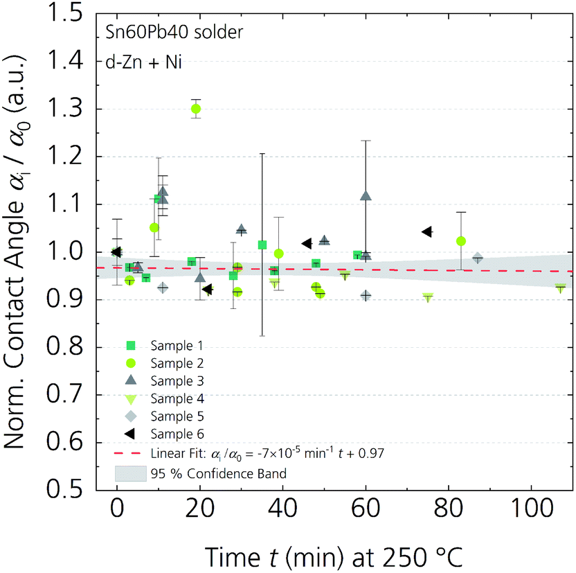 | ||
| Fig. 5 Change of the contact angle α of liquid Sn60Pb40 solder on d-Zn + Ni coated Al foil, measured at ambient air. Six identical samples with individual solder droplets of mSnPb = (11 ± 1) mg are tested. No dewetting (increase of αi) is observed within 100 min on a hotplate at 250 °C, as indicated by the linear fit yielding negligible slope. | ||
We could not detect any dewetting (significant change of αi/α0) within the total measurement time t of about 100 min. Since the soldering process for solar cells processed in an automated stringer lasts less than 20 s in total at an elevated temperature between TPreheating ≈ 50–170 °C and TSoldering ≈ 190–260 °C, the tested Ni coating should be easily solderable within the stringer for solar module production22 and similar applications.
To address the second aspect, we prepared metallographic cross sections of aged solder joints to analyse possible degradation effects on microstructural level. Fig. 6 shows SEM images at 20![[thin space (1/6-em)]](https://www.rsc.org/images/entities/char_2009.gif) 000× magnification of the relevant interfaces. Each image from (a to d) shows a part of the solder joint in Fig. 4b, aged for a certain time t at 85 °C and polished again before the measurement.
000× magnification of the relevant interfaces. Each image from (a to d) shows a part of the solder joint in Fig. 4b, aged for a certain time t at 85 °C and polished again before the measurement.
 | ||
| Fig. 6 SEM cross section images (20000× magnification) of solder joints: Al foil coated with d-Zn treatment and 8 min Ni plating, soldered manually with SnPbAg-coated Cu ribbons. The layers are schematically sketched on the left and after aging on the right. (a) Solder joint after 4.5 h aging at 85 °C at ambient air, (b) after 20 h aging, (c) after 500 h aging and (d) after 1000 h aging. | ||
In accordance with the constant adhesion, we could not find any crack formation or reoxidation at the interfaces. Vertical line scans (not shown here) are used to identify phase growth. When solid Al and Ni are in direct contact, they may form several intermetallic phases due to interdiffusion processes (Al3Ni, Al3Ni2, AlNi, Al3Ni5, AlNi3).29 In this binary system, the Ni-dominant phase AlNi3 is the most prominent phase to be built at temperatures T < 400 °C. Nevertheless, a small diffusion area of several 10 nm is detected at the Al/Ni interface, slightly growing for the aged samples, since the temperature during soldering was comparably low at (260 ± 20) °C.
Although not imaged in Fig. 6, the presence of Cu should be considered, due to the soldered Cu ribbon: the dissolved elements from the two different metal species (here Cu and Ni), can quickly diffuse across the molten solder and influence the interfacial reaction on the opposite side.30,31 Therefore, the present joints are so-called asymmetric Cu/Sn/Ni solder joints, including a Cu concentration gradient along the Sn-based solder joint. In our study, the exposure temperature of 85 °C is too low to detect a significant amount of Cu within the solder joint. Nevertheless, a thin Cu layer is formed on top of the Ni coating, directly after soldering. This layer slightly growths within 1000 hours of aging, as can be estimated from Fig. 6 and clarified by the sketches before (left) and after aging (right).
On a side note, the effect of the Zn treatment on the Al surface can be seen in these SEM cross section images: by increasing the roughness of the Al, the surface area is effectively increased.
To address the reliability aspect of the solder joint, we used isothermal aging at 85 °C. A set of solder joints with Sn62Pb36Ag2-coated Cu ribbons on d-Zn + Ni treated Al foil is fabricated and aged for 1000 hours at 85 °C in ambient air. After this treatment, the mechanical stability is characterised by 90° peel tests. Fig. 7 shows the results of the peel test measured after distinct time steps of aging. Any data point includes five peel tests of 150 mm evaluation length at different positions on the coated Al foils and dedicated standard deviation. The initial value of F/wt=0 = (5.5 ± 0.8) N mm−1 correlates well with the previous results in Fig. 3c, showing a mixture of fracture patterns on microstructural level. We could not measure any significant loss in adhesion within 1000 hours at 85 °C; only a slight decrease around 700 hours is observed, which however is far below the measurement uncertainty. The peel force stays above 4 N mm−1 without any change of the fracture pattern. This result indicates no reoxidation of the interfaces (Al/Ni and/or Ni/SnPbAg) and no increasing brittle intermetallic phase formation.
 | ||
| Fig. 7 Peel force of solder joints on 200 μm thick Al foil treated with d-Zn + Ni plating. Eight sets of samples are aged at 85 °C under ambient air and characterized after distinct time steps t. Each data point represents mean and standard deviation of five peel tests. | ||
Fracture mechanism
After the peel test, the analysis of the microstructure of the fracture pattern reveals information on the failure mechanism, the quality of the interfaces, voids and phase formation. Since no effect of aging is deducible, we present the analysis of the unaged sample, as shown in the inset of Fig. 3d.An area of 0.8 mm × 0.8 mm of the fracture is scanned by confocal scanning microscopy, resulting in a topography image given in Fig. 8a. From this part of the fracture, several investigations are carried out on microstructural level, presented in Fig. 8b–d and 9. All points of interest are labelled within the overview scan in Fig. 8a.
 | ||
| Fig. 8 Fracture pattern after a 90° peel test of Sn62Pb36Ag2 solder joint on d-Zn + Ni coated Al foil. (a) Topography scan with marked points of interest: line scans L1 & L2, tilted SEM images T1 & T2. (b) 30° tilted SEM image T1. (c) 30° tilted SEM image T2. (d) Corresponding EDX mapping for SEM image T2 in (c). | ||
 | ||
| Fig. 9 Fracture pattern after a 90° peel test of Sn62Pb36Ag2 solder joint on d-Zn + Ni coated Al foil. (a) Topography line scan L1 + SEM top view image. The graph shows the mean height profile of 21 line scans along the green line. (b) EDX line scan L2 + SEM top view image. | ||
Apart from the quality of the Ni coating, the failure could be caused by two fracture mechanism of the solder itself. The most probable fracture is along intermetallic phases since they are known to be brittle.32 As already shown earlier in this paper, no dominant intermetallic compounds (IMCs) are formed at the interface to the coating. Nevertheless, the binary system of Sn and Cu shows interdiffusion, already at room temperature. At the interface of the Cu ribbon, a thin Cu6Sn5 IMC of about 1 μm thickness could lead to an adhesive failure.33 In Fig. 8b, the remaining interface after peeling off the ribbon is shown. Here, an SEM image (T1), tilted by 30°, shows a close-up with two different failure modes. In the front of the image, the failure is adhesive between Ni coating and Al foil, in the back, the remaining solder layer is intact with an assumed failure at the Cu6Sn5 IMC.
The second fracture, correlated to the solder, may occur within the solder itself. This cohesive failure is only of minor importance in these samples. An example is shown in Fig. 8c by a 30° tilted SEM image (T2). In the back of the image, the remaining solder layer has a thickness of 5–20 μm, featuring a rough, grooved surface. This failure is supported by void formation e.g. flux remnants. For element correlation, the corresponding EDX mapping is given in Fig. 8d.
The two solder-related failure modes (adhesive at the interface to the Cu ribbon and cohesive within the solder),33 can be nicely correlated with height profiles to quantify the measurements. In Fig. 9a, the topography along a part of the fracture of Fig. 8a is shown. For the analysis of the height profile, 21 line scans along the green line L1 are evaluated. The profile is levelled to the Al substrate, which is visible in the marked region 1 in the diagram. The thickness of the solder coating after fabrication of the ribbon can vary between 10 μm and 20 μm. At the evaluated position of the solder joint, the total solder thickness is nearly 20 μm, shown in region 2. The cohesive failure within the solder, shown in Fig. 8c and d, is located on the right side of this part of the SEM top view image in region 5 and 6, indicated by the area T2. The height is measured to be about 10 μm, also visible in region 3. In the case of an adhesive failure of the coating, the bare Al foil is visible (cf. region 1, 4 and 6).
Fig. 9b shows an EDX line scan (L2) with the corresponding section of the SEM top view image. On the left, the bare Al surface can be seen (magenta in the line scan), where the Al/Ni interface failed during the peel test. This failure may be supported by impurities on top of the Al foil or by reoxidation after plating due to oxygen or Al diffusion. On the right, the typical morphology of the Ni layer is observed (cyan, cf. Fig. 3e). Remnants of solder (Sn in green, Pb in blue) and a crack within the Ni layer are also visible. The dominant failure mechanism in this region is along the Ni/Sn interface, presumably due to an inhomogeneous soldering process due to manual contact soldering.
The detailed analysis of the fracture pattern shows no dominant failure mechanism for solder joints on Ni-coated Al foils after a 90° peel test. All parts of the solder joints perform similar; no material weakness is observed. This implies an optimal material combination for joining a Cu ribbon to an Al substrate by a fast soldering process.
Conclusions and outlook
Direct contacting of Al substrates by soldering is challenging, especially for very short soldering processes at ambient air. To realize a solder connection on Al, we used single and double zincate treatment to modify the surface of 200 μm thick Al foils. Electroless plating of Ni provides a homogeneous solderable Ni layer, which can be contacted with Sn-based solders for process times <5 s. We performed detailed analysis on the initial performance of the solder joints, including mechanical strength after soldering and reliability during isothermal aging. The focus is set on solder joints on Al foils, treated with a double zincate process for 30 s + (15–30) s and subsequent Ni plating for 8 min. Since, the Ni surface provides good wettability (contact angle α < 60° for liquid Sn60Pb40), the mechanical stability of the joints, tested by a 90° peel test, is very good (F/w ≈ 5.6 N mm−1). Both properties show a reliable performance when exposed to higher temperatures (250 °C, 85 °C) for longer times (100 min, 1000 h).In contrast to known literature, the innovation of our work is a detailed analysis of the solder joints on microstructural level and their long-term stability. Therefore, we investigate metallographic cross sections of the solder joints and the fracture pattern after the peel test. SEM and EDX investigations show small diffusion zones at the interfaces Al/Ni and Sn/Ni and no brittle intermetallic phase formation. For all joints after the peel test, as well as the aged samples, a mixed fracture pattern with different fracture modes is observed. Therefore, the quality of all interfaces (Al/Ni, Ni/Sn, Sn/Cu) is similar and highly reliable, resulting in excellent and uniform mean peel forces >4 N mm−1. This shows the high potential of this material combination and the suitability of the very simple and short soldering process to yield strong and reliable solder joints on Al foils.
The wet chemical coating (Zn treatment and electroless Ni plating) has been widely reported in literature and can be easily executed on inline or batch tools.11,15,17,21,34 For a higher throughput for the investigated coating in this work, the Ni plating time could be further reduced, depending on the quality of the Zn layer and the desired Ni thickness. Since the soldering time is really short (<5 s), the used solder alloy has to be eutectic or even near-eutectic to ensure fast and homogeneous liquidation and solidification. Therefore, Sn-based alloys with Tliq < 200 °C may be advantageous.
For the interconnection of silicon solar cells, this coating process might be suitable, as the rear electrode mostly consist of Al, either screen printed paste, PVD Al35 or Al foil.36,37 Since the presented wet chemical coating is a low-temperature process, it could also be used to coat temperature sensitive devices with Al components.
Conflicts of interest
There are no conflicts to declare.Acknowledgements
The German Ministry for Economic Affairs and Energy is gratefully acknowledged for financially supporting this work within the project “FolMet-Modul” (contract number 0325892). The authors thank all co-workers at Fraunhofer ISE who contributed to this investigation.Notes and references
- Fundamentals of aluminium metallurgy. Production, processing and applications, ed. R. N. Lumley, Woodhead Publishing, Cambridge, MA, 2018 Search PubMed.
- G. Liu and D. B. Müller, Addressing sustainability in the aluminum industry: a critical review of life cycle assessments, J. Cleaner Prod., 2012, 35, 108–117 CrossRef.
- J. R. Davis, Aluminum and Aluminum Alloys, ASM International, 1993 Search PubMed.
- T. Campbell, R. K. Kalia, A. Nakano, P. Vashishta, S. Ogata and S. Rodgers, Dynamics of Oxidation of Aluminum Nanoclusters using Variable Charge Molecular-Dynamics Simulations on Parallel Computers, Phys. Rev. Lett., 1999, 82, 4866–4869 CrossRef CAS.
- C. E. Brittin, Vacuum brazing of aluminum alloy workpieces, US Pat., US4886449A, 1989.
- C. J. Miller, Aluminum brazing, US Pat., US3321828A, 1967.
- H. T. Zhang, J. C. Feng, P. He and H. Hackl, Interfacial microstructure and mechanical properties of aluminium–zinc-coated steel joints made by a modified metal inert gas welding–brazing process, Mater. Charact., 2007, 58, 588–592 CrossRef CAS.
- W. B. Guo, X. S. Leng, J. C. Yan and Y. M. Tan, Ultrasonic Soldering Aluminum at Low Temperature, Weld. J., 2015, 94, 189–195 Search PubMed.
- C. A. Huntington and T. W. Eagar, Laser Welding of Aluminum and Aluminum Alloys, Weld. J., 1983, 62, 105–107 Search PubMed.
- A. De Rose, A. Kraft, U. Eitner and M. Nowottnick, Solder Joint Analysis on Coated Aluminum for Silicon Solar Cell Interconnection, in 41st International Spring Seminar on Electronics Technology (ISSE), ed. IEEE, IEEE, 2018, pp. 1–6 Search PubMed.
- M. Kamp, J. Bartsch, G. Cimiotti, R. Keding, A. Zogaj, C. Reichel, A. Kalio, M. Glatthaar and S. W. Glunz, Zincate processes for silicon solar cell metallization, Sol. Energy Mater. Sol. Cells, 2014, 120, 332–338 CrossRef CAS.
- S. Court, C. Ponce de León, J. R. Smith and F. C. Walsh, Monitoring of zincate pre-treatment of aluminium prior to electroless nickel plating, Trans. IMF, 2017, 95, 97–105 CrossRef CAS.
- E. H. Hewitson, Process of Coating Aluminum Surfaces, US Pat., US1627900A, 1927.
- H. Nagel, M. Kamp, D. Eberlein, A. Kraft, J. Bartsch, M. Glatthaar and S. W. Glunz, Enabling Solderability of PVD Al Rear Contacts on High-Efficiency Crystalline Silicon Solar Cells by Wet Chemical Treatment, in Proceedings of the 32nd European Photovoltaic Solar Energy Conference and Exhibition, 2016, pp. 48–52 Search PubMed.
- K. Azumi, T. Yugiri, M. Seo and S. Fujimoto, Double Zincate Pretreatment of Sputter-Deposited Al Films, J. Electrochem. Soc., 2001, 148, C433–C438 CrossRef CAS.
- M. Hino, K. Murakami, M. Hiramatsu, K. Chen, A. Saijo and T. Kanadani, Effect of Zincate Treatment on Adhesion of Electroless Ni-P Plated Film for 2017 Aluminum Alloy, Mater. Trans., 2005, 46, 2169–2175 CrossRef CAS.
- F. Keller and W. G. Zelley, Conditioning Aluminum Alloys for Electroplating, J. Electrochem. Soc., 1949, 97, 143–151 CrossRef.
- M. Hino, K. Murakami, Y. Mitooka, K. Muraoka, R. Furukawa and T. Kanadani, Effect of Zincate Treatment on Adhesion of Electroless Ni-P Coating onto Various Aluminum Alloys, Mater. Trans., 2009, 50, 2235–2241 CrossRef CAS.
- W. G. Zelley, Formation of Immersion Zinc Coatings on Aluminum, J. Electrochem. Soc., 1953, 100, 328–333 CrossRef CAS.
- CRC Handbook of Chemistry and Physics, ed. D. R. Lide, CRC Press, Boca Raton, Florida, 2005 Search PubMed.
- M. Kamp, Electrochemical process for metallization of novel silicon solar cells, PhD thesis, Albert-Ludwigs-Universität Freiburg im Breisgau, 2016.
- A. De Rose, T. Geipel, D. Eberlein, A. Kraft and M. Nowottnick, Interconnection of Silicon Heterojunction Solar Cells by Infrared Soldering - Solder Joint Analysis and Temperature Study, in Proceedings of the 36th European Photovoltaic Solar Energy Conference and Exhibition (EU PVSEC), 2019, pp. 229–234 Search PubMed.
- RoHS-Richtlinie 2011/65/EU: Beschränkung der Verwendung bestimmter gefährlicher Stoffe in Elektro- und Elektronikgeräten, 2011 Search PubMed.
- P. Schmitt, D. Eberlein, P. Voos, M. Tranitz and H. Wirth, Metallographic preparation of solar cell samples for quality assurance and material evaluation, Energy Procedia, 2011, 8, 402–408 CrossRef CAS.
- Y. Yuan and T. R. Lee, in Surface science techniques, ed. G. Bracco and B. Holst, Springer Berlin Heidelberg, 2013, pp. 3–34 Search PubMed.
- R. J. Klein Wassink, Soldering in Electronics, Leuze, Saulgau/Württ, 2nd edn, 1991 Search PubMed.
- Deutsches Institut für Normung e.V. (DIN), Solarzellen - Datenblattangaben und Angaben zum Produkt für kristalline Silicium-Solarzellen, EN 50461, Beuth Verlag GmbH, 2007 Search PubMed.
- International Electrotechnical Commission (IEC), Terrestrial photovoltaic (PV) modules – Design qualification and type approval – Part 2: Test procedures, IEC, 2016, p. 61215-2 Search PubMed.
- H. Baker, Alloy Phase Diagrams, ASM Handbook, ASM International, 3rd edn, 2016 Search PubMed.
- S. J. Wang and C. Y. Liu, Asymmetrical solder microstructure in Ni/Sn/Cu solder joint, Scr. Mater., 2006, 55, 347–350 CrossRef CAS.
- H. W. Tseng, S. J. Wang and C. Y. Liu, Cross-interaction effect in the Ni/Sn/Cu solder joints, in 11th Electronics Packaging Technology Conference, 2009, ed. IEEE Reliability/CPMT/ED Singapore, IEEE, Piscataway, NJ, 2009, pp. 325–330 Search PubMed.
- T. Geipel, M. Moeller, J. Walter, A. Kraft and U. Eitner, Intermetallic compounds in solar cell interconnections, Sol. Energy Mater. Sol. Cells, 2017, 159, 370–388 CrossRef CAS.
- J. A. von Fraunhofer, Adhesion and cohesion, Int. J. Dent., 2012, 2012, 951324 Search PubMed.
- A. De Rose, M. Kamp, G. Mikolasch, A. Kraft and M. Nowottnick, Adhesion improvement for solder interconnection of wet chemically coated aluminum surfaces, in AIP Conference Proceedings 2156, AIP Publishing, 020016th edn, 2019, p. 020014 Search PubMed.
- J. Kumm, R. V. Chacko, H. Samadi, P. Hartmann, D. Eberlein and A. Wolf, Long-term and Annealing Stable, Solderable PVD Metallization with Optimized Al Diffusion Barrier, Energy Procedia, 2015, 77, 374–381 CrossRef CAS.
- A. De Rose, A. Kraft, S. Gledhill, M. T. Ali, T. Kroyer, C. Pscherer, M. Graf, J. Nekarda and U. Eitner, Solder Interconnection of Aluminum Foil Rear Side Metallization for Passivated Emitter and Rear Solar Cell, in 7th Workshop on Metallization and Interconnection for Crystalline Silicon Solar Cells, Konstanz, Germany, 2017 Search PubMed.
- J. F. Nekarda, A. Grohe, O. Schultz and R. Preu, Aluminum Foil as Back Side Metallization, in Proceedings of the 22nd European Photovoltaic Solar Energy Conference and Exhibition, 2007, pp. 1499–1501 Search PubMed.
| This journal is © The Royal Society of Chemistry 2020 |