
 Open Access Article
 This Open Access Article is licensed under a Creative Commons Attribution-Non Commercial 3.0 Unported Licence
Facile all-dip-coating deposition of highly efficient (CH3)3NPbI3−xClx perovskite materials from aqueous non-halide lead precursor†
Muhammad Adnan a,
Zobia Irshada and
Jae Kwan Lee*ab
a,
Zobia Irshada and
Jae Kwan Lee*ab
aDepartment of Chemistry, Graduate School, Chosun University, Gwangju, 61452, Republic of Korea. E-mail: chemedujk@chosun.ac.kr; Fax: +82 62 232 8122; Tel: +82 62 230 7319
bDepartment of Chemistry Education, Chosun University, Gwangju, 61452, Republic of Korea
First published on 5th August 2020
Abstract
Sequential all-dip-coating deposition of (CH3)3NPbI3−xClx perovskite materials was conducted in an aqueous nonhalide lead precursor solution, which was followed by that in a (CH3)3NI and (CH3)3NCl mixed solution as part of a facile, cost-effective, and environmentally benign manufacturing process for high-efficiency perovskite solar cells. The (CH3)3NPbI3−xClx perovskite layers deposited via the proposed process were constructed with a Cl/I ratio below ∼3%, indicating the partial insertion of Cl into the (CH3)3NPbI3 perovskite lattice. The amount of Cl inserted was readily modulated by varying the (CH3)3NCl concentration in the (CH3)3NI/(CH3)3NCl mixed solution. Incorporating a small amount of Cl led to significant improvements in the surface morphology and crystallinity of the perovskite layer as compared to (CH3)3NPbI3 fabricated under the same conditions. The perovskite solar cell devices with these (CH3)3NPbI3−xClx perovskite films exhibited superior device performances and stabilities, resulting in an outstanding power conversion efficiency of ∼15.3%. Results show that the fabrication of (CH3)3NPbI3−xClx perovskite material with an aqueous nonhalide lead precursor is more efficient than conventional spin-casting approach with detrimental organic solvents.
1. Introduction
Recently, the use of organic–inorganic lead halide perovskite materials has attracted significant attention owing to the excellent power conversion efficiencies (PCEs) of perovskite solar cells (PrSCs), which have been proposed as potential alternatives for conventional silicon solar cells.1,2 Particularly, alkylammonium lead halides such as (RNH3)PbX3 (R = alkyl, X = Cl, Br, I), when used as direct-band-gap materials, manifest exceptional electron/hole conduction and photosensitizer performances by occupying the hybrid organic–inorganic perovskite cores to provide promising high PCEs in PrSCs.3,4 These perovskite materials have been developed extensively using a variety of deposition strategies listed as follows: (1) the spin casting of the lead source PbX2 followed by reaction with an alkylammonium halide such as an methylammonium iodide (CH3NH3I, MAI) by dipping in a solution, spin casting, or vacuum deposition5,6 and (2) direct spin-casting of a perovskite precursor solution with thermal annealing, interfacial engineering, solvent engineering, or adducts.7,8 However, the spin casting deposition techniques of perovskite materials frequently limit the substrate size, causing a reduction in the active area. Toxicity due to high-polar aprotic organic solvents, e.g., dimethyl formamide and dimethyl sulfoxide, which are used due to the poor solubility of lead halide precursors is also an important issue.Very recently, we developed a simple sequential dip-coating (SDC) deposition approach applicable for large areas to fabricate an efficient (CH3NH3)PbI3 (MAPbI3) perovskite film using an aqueous non-halide lead precursor such as Pb(NO3)2, which was employed owing to its good compatibility with environmentally benign and low-cost non-toxic solvents such as water.9,10 The Pb(NO3)2 layer adsorbed spontaneously on the ZnO substrate by the SDC process leads to a stable and efficient MAPbI3 perovskite crystalline structure from the successive solid-state ion-exchange and reaction (SSIER) with MAI. The MAPbI3 perovskite layers fabricated by this approach have satisfactorily high PCEs in PrSCs. However, it is challenging yet essential for commercial applications to achieve better performances than those obtained by spin-casting deposition. Therefore, we aim to develop a simple dip-coating deposition method for mixed halide-based perovskite materials, especially MAPbI3−xClx, which increased the PCEs to above 20% of that of PrSCs.11 The MAPbI3−xClx perovskite materials bare more attractive owing to their higher charge carrier mobility and longer charge carrier diffusion length than MAPbI3.3,5,12 These have hitherto been prepared by the reaction of PbI2 and MACl (or PbCl2 and MAI), but currently, the preparation is done by inserting a small amount of Cl in the MAPbI3 perovskite lattice.7,13,14
In this study, we demonstrate a facile, cost-effective, and environmentally benign approach to prepare efficient MAPbI3−xClx perovskite films from aqueous non-halide lead precursors by a simple all-dip-coating deposition process for the first time. This was readily demonstrated by sequentially dipping a thin ZnO/TiO2 bilayer deposited substrate in an aqueous Pb(NO3)2 solution and subsequently, in an MAI and MACl mixed solution. Interestingly, we found that the MAPbI3−xClx perovskite layers deposited via a simple dip-coating process were constructed with a Cl/I ratio below ∼3%, indicating the partial insertion of Cl into the MAPbI3 perovskite lattice. The inserted amounts of Cl could be readily modulated by varying the MACl concentration in the MAI and MACl mixed solution. Despite the small amount of Cl incorporation, this might lead to significant improvements in the surface morphology and crystallinity of the MAPbI3−xClx perovskite layers compared to those of MAPbI3 fabricated under the same conditions.12,15,16 Consequently, this SDC approach enables the fabrication of the most efficient MAPbI3−xClx perovskite materials with an aqueous non-halide lead precursor, in contrast to the conventional spin-casting approach that uses detrimental organic solvents (DMF and DMSO). The main purpose behind this work is to avoid the toxicity of hazardous DMF and DMSO solvents to dissolve the lead halide precursor and to focus on the usage of aqueous non-halide lead precursor to prepare an efficient perovskite films which didn't obey the restrictions of substrate size.9–19 The PrSC devices with these perovskite films exhibited superior device performances and stabilities, resulting in an outstanding PCE of ∼15.3%. Fig. 1 shows (a) a schematic description of MAPbI3−xClx perovskite material deposited by sequentially dipping a ZnO-covered TiO2/fluorine-doped tin oxide (FTO) substrate in aqueous Pb(NO3)2 and MACl/MAI mixed solutions followed by repetition of the SSIER process between annealing at 100 °C and dipping in MACl/MAI mixed solutions and Fig. 1(b) a PrSC architecture used in this study. These are also compared to those of MAPbI3.
 | ||
| Fig. 1 (a) Schematic description of MAPbI3 and MAPbI3−xClx perovskite material deposited by sequentially all-dip-coating in aqueous Pb(NO3)2 and MAI and MACl/MAI mixed solutions, respectively, followed by repetition of the SSIER process and (b) a PrSC architecture used in this study. | ||
2. Experimental section
2.1 Materials
MAI and MACl were prepared according to a previously reported method.4,10 All reagents, including 4-tert-butylpyridine (t-BPy) and lithium bis(trifluoromethanesulfonyl)imide (Li-TFSI) were purchased from Sigma-Aldrich, TCI, and Alfa Aesar. The solvents were also purified using appropriate methods. The required quantity of 2,2′,7,7′-tetrakis(N,N-di-4-methoxyphenylamino)-9,9′-spirobifluorene (spiro-OMeTAD) was obtained from Solaronix. The ZnO sol–gel was synthesized by reacting zinc acetate dihydrate (1.6 g, Sigma Aldrich, 99.9%), ethanolamine (0.5 g, Sigma Aldrich, 99.5%) and 2-methoxy-ethanol (10 ml, Sigma Aldrich, 99.8%) for 4 h at room temperature.202.2 Fabrication of MAPbI3−xClx perovskite films
To fabricate MAPbI3−xClx perovskite films from aqueous Pb(NO3)2, we employed a SDC followed by SSIER repetition. In a typical process, a FTO substrates were first dipped into a 0.1 M solution of Pb(NO3)2 (Sigma-Aldrich, 99.9%) dissolved in ethanol (EtOH)/water (2![[thin space (1/6-em)]](https://www.rsc.org/images/entities/char_2009.gif) :1, v/v) for 30 s. The substrate was washed using deionized water and ethanol and then annealed at 120 °C for 10 min, resulting in a highly transparent film over the substrate. The MAI solution was prepared at 0.1 M concentration in isopropanol (IPA). The MACl/MAI mixed solutions were also prepared by adding various concentrations of MACl (0.045, 0.075, and 0.090 M) in the 0.1 M MAI solution. The substrate was dipped into MAI (or MACl/MAI) dissolved in isopropanol (IPA) for 30 s and then washed with chloroform and diethyl ether and annealed at 100 °C for 10 m. The above procedure formed one SSIER cycle. These films were subjected to SSIER repetitions to complete the reaction between Pb(NO3)2 and MACl/MAI.
:1, v/v) for 30 s. The substrate was washed using deionized water and ethanol and then annealed at 120 °C for 10 min, resulting in a highly transparent film over the substrate. The MAI solution was prepared at 0.1 M concentration in isopropanol (IPA). The MACl/MAI mixed solutions were also prepared by adding various concentrations of MACl (0.045, 0.075, and 0.090 M) in the 0.1 M MAI solution. The substrate was dipped into MAI (or MACl/MAI) dissolved in isopropanol (IPA) for 30 s and then washed with chloroform and diethyl ether and annealed at 100 °C for 10 m. The above procedure formed one SSIER cycle. These films were subjected to SSIER repetitions to complete the reaction between Pb(NO3)2 and MACl/MAI.
2.3 PrSC device fabrication
The c-TiO2 layer was spin-cast on the substrate with a titanium(IV) diisopropoxide bis(acetylacetonate) solution diluted in butanol (1:10, v/v) and then annealed at 120 °C for 5 min to avoid direct contact between the FTO surface and hole transporting material (HTM). Over the c-TiO2 layer, the ZnO layer was spin-cast with 0.75 M ZnO sol–gel solutions at 5000 rpm for 30 s (ref. 19) followed by annealing at 300 °C for 1 h. The MAPbI3 and MAPbI3−xClx perovskite layers were fabricated according to the aforementioned method. The spiro-OMeTAD HTM was deposited via spin-coating at 3000 rpm for 30 s; the HTM solution was prepared by dissolving 29 mg of spiro-OMeTAD, 7 μL of 170 mg mL−1 Li-TFSI in acetonitrile, and 11 μL of t-BPy.9,10 Finally, device fabrication was completed by thermal evaporation of a thin MoO3 layer and thick Ag layer on top of the HTM film under reduced pressure (less than 10−6 Torr).
2.4 Measurements and instrument
The absorption spectra were recorded on a PerkinElmer Lambda 2S ultraviolet (UV)-visible spectrometer. The surface morphologies were imaged using a field emission scanning electron microscope (FESEM, Nova Nano-SEM 450, FEI, Netherlands). Elemental analysis and presence of newly formed chemical bonds with Pb, I, and Cl in perovskite compounds were performed using X-ray photoelectron spectroscopy (XPS, AXIS-NOVA, KratosInc, USA). The perovskite crystallinities of the MAPbI3 layers were investigated using X-ray diffraction (XRD, D/Max2500 V/PC, Rigaku Corp, Japan). The solar cell efficiencies were characterized under simulated 100 mW cm−1 AM 1.5G irradiation from a Xe arc lamp with an AM 1.5 global filter. The simulator irradiance was characterized using a calibrated spectrometer; the illumination intensity was set using a silicon diode with an integrated KG1 optical filter certified by the National Renewable Energy Laboratory. The spectral mismatch factors were calculated to be less than 5% for each device. The short circuit currents were also found to be within 5% of the values calculated using the integrated external quantum efficiency (EQE) spectra and solar spectrum. The applied potential and cell currents were measured using a Keithley 2400 model digital source meter. The J–V curves were measured at a voltage settling time of 100 ms. The EQEs were measured by under-filling the device area using a reflective microscope objective to focus the light output from a 75 W Xe lamp, monochromator, and optical chopper; the photocurrent was measured using a lock-in amplifier; and the absolute photon flux was determined using a calibrated silicon photodiode and was recorded for 5 s per point (80 points) from 360 to 900 nm. In the J–V curves hysteresis tests, a forward scan indicates the measurement of the sweeping voltage from short circuit to forward bias, whereas a backward scan indicates a sweep in the opposite direction. To explore the active area of the device and avoid the scatter effects of the edges, a non-reflective metal plate mask with an aperture of 4.5 mm2 was used for the solar cells.3. Results and discussion
For the deposition of the MAPbI3−xClx perovskite layer by a simple dip-coating process, as shown in Fig. 1a, we first fabricated a Pb precursor layer by dipping the substrate in an aqueous Pb(NO3)2 solution. The Pb(NO3)2 was unprecedently adsorbed on the ZnO surface and then rapidly changed to dark brown-coloured films upon exposure to the MAI solution and MACl/MAI mixed solution even in a very short time of 30 s, indicating the formation of MAPbI3 and MAPbI3−xClx perovskite materials, respectively. However, these perovskite films rapidly decomposed, showing a change to a yellowish film corresponding to the crystalline morphology of PbI2 during solvent drying at 100 °C, even below 20% relative humidity. We have speculated that MAPbI3 and MAPbI3−xClx perovskite materials could participate in ion-exchange reactions between the unreacted Pb(NO3)2 even in the solid state, and this is defined as the SSIER process.9,10 We attempted to efficiently achieve more stable perovskite layers by applying SSIER cycles. Interestingly, we found that the perovskite film fabricated via repetitive SSIERs in MACl/MAI mixed solution exhibited much darker blackish color compared to that in MAI solution, as shown in Fig. 1. This seemed to be a different perovskite material with the MAPbI3 perovskite structure that forms upon exposure to the MAI solution of the Pb(NO3)2 layer. Therefore, in this study, we prepared three types of MACl and MAI mixture solutions: 0.45-MACl/MAI, 0.75-MACl/MAI, and 0.90-MACl/MAI by adding MACl of 0.045, 0.075, and 0.090 M, respectively, in MAI solution of 0.1 M, which were compared to those in MAI solution without MACl. The perovskite material layers fabricated by a simple dip-coating process using these MACl/MAI mixed solutions presented much better stability without decomposing into PbI2 as of five SSIER cycles, as shown in Fig. S1–S4.†Fig. 2 shows the (a and b) UV-vis absorption and (c) photoluminescence (PL) spectra for MAPbI3 and MAPbI3−xClx perovskite material films deposited on ZnO/c-TiO2/FTO, in which simple all-dip-coating approaches were used under the five SSIER cycles. All perovskite layers were prepared in air by controlling the humidity of less than 20%. These films show the typical absorption behaviours of MAPbI3 and MAPbI3−xClx perovskite materials with onset points in the vicinity of 790 nm (optical band gap < 1.5 eV). The higher MACl concentration in the MACl/MAI mixture led to darker blackish-colored and turbid perovskite films, thereby providing nonuniform absorption behaviour by light scattering in the UV-vis spectra shown in Fig. 1a. All MAPbI3−xClx perovskite materials prepared in the MACl/MAI mixed solution seemed to exhibit a higher light-absorption efficiency at a wavelength of 750 nm than MAPbI3 subjected to the MAI solution when their baselines were adjusted to a ∼850 nm (Fig. 2b), indicating better crystalline morphology of perovskite films. Also, all MAPbI3−xClx perovskite materials prepared in the MACl/MAI mixed solution exhibited the lower PL intensities than MAPbI3 subjected to the MAI solution as shown in Fig. 2c. This indicates that perovskite materials prepared in the MACl/MAI mixed solutions show better charge transfer into the ZnO/c-TiO2 ETL layer than those in the MAI solution.
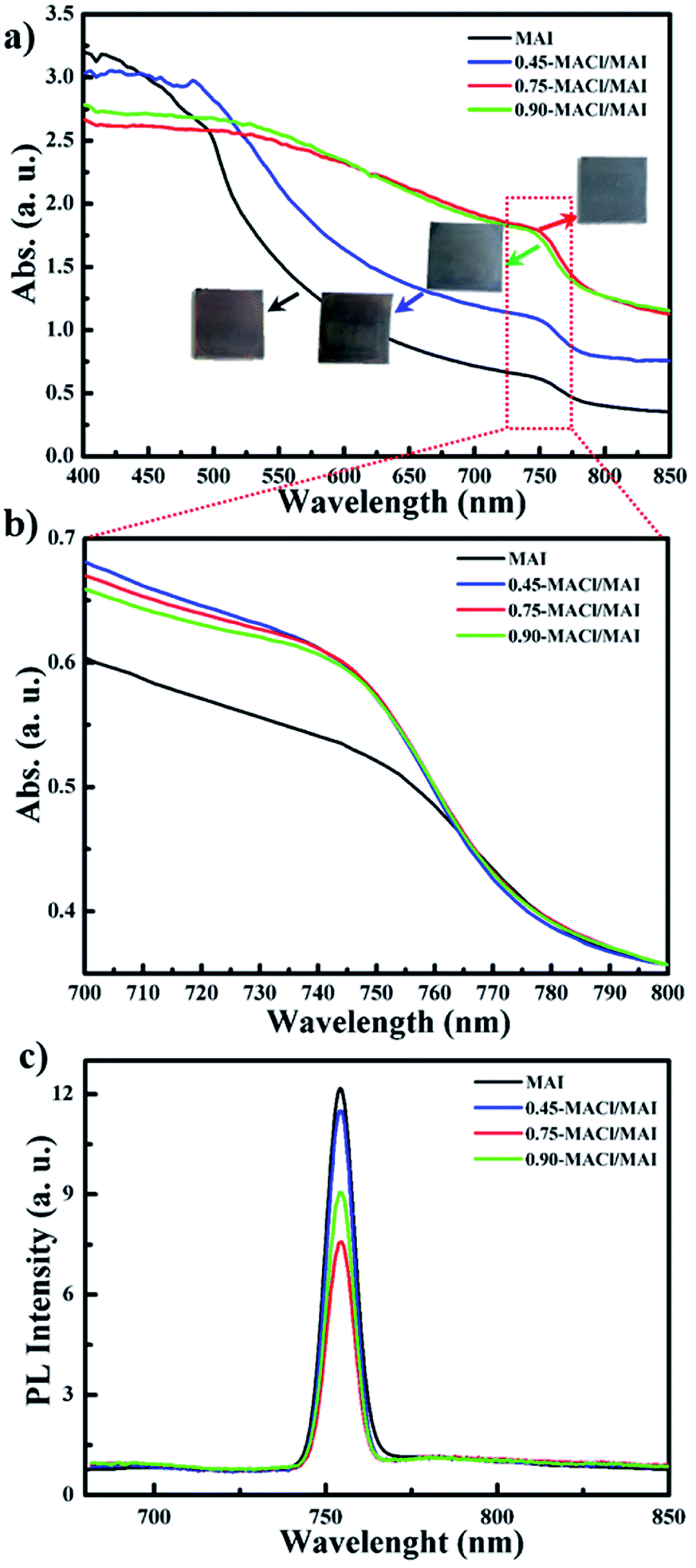 | ||
| Fig. 2 (a and b) UV-Vis absorption and (c) photoluminescence (PL) spectra for MAPbI3 and MAPbI3–Clx perovskite material films deposited on ZnO/c-TiO2/FTO, in which simple all-dip-coating approaches were used under the five SSIER cycles. | ||
Meanwhile, the PL intensities of their perovskite films were significantly affected by the MACl concentration of the MACl/MAI mixed solution. Interestingly, it was observed that the perovskite materials prepared in 0.75-MACl/MAI presented lower PL intensities compared to those prepared with 0.45-MACl/MAI and 0.90-MACl/MAI. These results indicate that the perovskite materials deposited by a simple all-dip-coating process in aqueous Pb(NO3)2 solution and MACl/MAI mixed solution might have the characteristics of MAPbI3−xClx perovskite structure in which the Cl composition is closely related to the MACl concentration. Therefore, we investigated the surface morphologies, crystallinity, and atomic compositions of these perovskite material films. Fig. 3 shows FESEM images of the surface morphologies of MAPbI3 prepared in (a) MAI and MAPbI3−xClx perovskite materials prepared in (b) 0.45-MACl/MAI, (c) 0.75-MACl/MAI, and (d) 0.90-MACl/MAI, respectively, under the same conditions. They could be compared with those of the (e) Pb(NO3)2 layer adsorbed on (f) ZnO/c-TiO2/FTO substrate.
 | ||
| Fig. 3 FESEM images of the surface morphologies of MAPbI3 prepared in (a) MAI and MAPbI3−xClx perovskite materials prepared in (b) 0.45-MACl/MAI, (c) 0.75-MACl/MAI, and (d) 0.90-MACl/MAI, respectively, under the same conditions, and (e) Pb(NO3)2 layer adsorbed on (f) ZnO/c-TiO2/FTO substrate. | ||
The Pb(NO3)2 deposited by dipping into an aqueous Pb(NO3)2 solution presented well surface coverage with a particulate morphology on the ZnO/c-TiO2/FTO substrate (Fig. 3e). As shown in Fig. 3a, the MAPbI3 perovskite film fabricated via SDC of this Pb(NO3)2 layer in MAI solution followed by five SSIER cycles exhibited a structural morphology with submicron-sized cubic-like crystal lumps grown from Pb(NO3)2, but it shows distinct grain boundaries and rather sparse surface coverages on ZnO/c-TiO2/FTO substrates. The grain boundaries can interrupt efficient charge transport, and inadequate surface coverage can lead to interfacial recombination between the metal oxides and HTMs, resulting in the poor performance of PrSC devices. Meanwhile, the MAPbI3−xClx perovskite materials fabricated with 0.45-MACl/MAI, 0.75-MACl/MAI, and 0.90-MACl/MAI exhibited a blunter structural morphology with a well-adhering grain boundary and much better complete surface coverage than MAPbI3 prepared under the same conditions as shown in Fig. 3, thereby providing better performance of PrSC devices.
To clarify the origin of these variation in the surface morphology, XPS and XRD analyses were carried out to investigate the superficial chemical composition and crystallinity. Fig. 4a shows the XPS spectra of MAPbI3 prepared in MAI (black line) and MAPbI3−xClx perovskite materials prepared in 0.45-MACl/MAI (blue line), 0.75-MACl/MAI (red line), and 0.90-MACl/MAI (green line), respectively. All the perovskite materials show common peaks at 143 (and 138) and 616 eV, which correspond to the peak Pb 4f5/2 (4f7/2) and I 3d.4,16,21 Interestingly, in the case of MAPbI3−xClx perovskite materials, an additional signal was detected at 198–202 eV for Cl 2p, as clearly seen even at very low intensities from the XPS, as shown in Fig. 4c. Furthermore, the elemental quantitative data of Pb, I, and Cl were obtained from XPS, which is summarized in Table S1.† The Cl-contents in MAPbI3−xClx perovskite materials were determined to b 0.63, 1.18, and 3.14% (%ratio of Cl/I) in 0.45-MACl/MAI, 0.75-MACl/MAI, and 0.90-MACl/MAI, respectively. Although a similar concentration of MACl to that of MAI was adapted in a mixed solution, the low content of Cl in MAPbI3−xClx perovskite materials might be caused by the formation kinetics of MAPbI3 perovskite structure being much higher than that of MAPbI3−xClx perovskite structure. This might lead to Cl incorporation into MAPbI3 at relatively low concentrations. Additionally, the MAPbI3−xClx perovskite structure fabricated by this SDC approach might be readily modulated using the incorporated Cl content by varying the concentration of MACl in solution mixed with MAI, even as the maximum concentration of Cl that can be introduced into MAPbI3 perovskite through conventional spin-casting method has been limited to below 4% (Cl/I), in which Cl doping might be possible that the unusual halogen ionic radii difference may interferes with the origination of a continual solid solution. Regardless the materials band gap, any small amount of Cl incorporation into the MAI solution may increase the charge transportation within the perovskite layer which ultimately helps to boost the device performances, accordingly.22–24
 | ||
| Fig. 4 (a) XPS spectra and (b) XRD patterns of MAPbI3 prepared with MAI (black line) and MAPbI3−xClx perovskite materials prepared with 0.45-MACl/MAI (blue line), 0.75-MACl/MAI (red line), and 0.90-MACl/MAI (green line), respectively and (c) Cl 2p spectra in MAPbI3−xClx perovskite materials (d) correlated their perovskite conversions. | ||
The XRD patterns of MAPbI3 prepared with MAI (black line) and MAPbI3−xClx perovskite materials prepared with 0.45-MACl/MAI (blue line), 0.75-MACl/MAI (red line), and 0.90-MACl/MAI (green line), respectively and correlated their perovskite conversions (Fig. 4b and d). All the XRD patterns of these perovskite materials indicated typical MAPbI3 crystalline structures with an intense peak of (100) at 2θ = 14.2° (ref. 25) and no peaks related to the MAPbCl3 perovskite crystal structure at 2θ = 15.4° (ref. 16) as shown in Fig. 4b. This indicates that the MAPbI3−xClx materials fabricated via SDC in aqueous Pb(NO3)2 solution and in MACl/MAI mixed solution might have perovskite structures inserted partially into the MAPbI3 perovskite lattice of Cl, like a dopant. Based on the XRD patterns, the conversion of MAPbI3 (CMAPbI3) could be qualitatively defined using the peak intensities of PbI2 and MAPbI3 at 2θ = 12.7° and 14.2°, respectively25
| CMAPbI3 = I12.7°/(I12.7° + I14.2°) | (1) |
As shown in Fig. 4d, the CMAPbI3 values could be dependent on the concentrations of MACl in the MACl/MAI mixed solution. The MAPbI3−xClx perovskite materials prepared in 0.75-MACl/MAI gave higher conversion values for MAPbI3 perovskite generated from PbI2 compared to those in MAI, 0.45-MACl/MAI and 0.90-MACl/MAI. This indicates that a high concentration of MACl in the 0.90-MACl/MAI mixed solution might interrupt the MAPbI3 perovskite formation by retarding the reaction between PbI2 and MAI. From these results, despite the existence of a very small amount of Cl in the perovskite film, we found that Cl incorporation can induce a significant improvement in the surface morphologies and crystallinities, as shown in Fig. 3 and 4, which can ultimately lead to improved device performance of the PrSCs.
Subsequently, we evaluated the photovoltaic performances of PrSCs with MAPbI3 and MAPbI3−xClx perovskite material films deposited on the thin ZnO/c-TiO2 bilayer ETL by a simple all-dip-coating approach in MAI and MACl/MAI mixed solutions, respectively, and an aqueous Pb(NO3)2 solution. The PrSC devices were constructed with an n–i–p configuration of FTO/c-TiO2/ZnO/MAPbI3 (or MAPbI3−xClx)/HTM/MoO3/Ag. The conductivity and efficiency of spiro-OMeTAD used as the HTM were improved after doping with additives such as t-BPy and Li-TFSI.5,9 We determined the optimum photovoltaic performance by comparing more than 200 individual PrSC devices. Fig. 5a shows the current–voltage (J–V) curves under an AM 1.5 irradiation (100 mW cm−1) for most efficient PrSCs based on MAPbI3−xClx perovskite layers fabricated via a simple all-dip-coating approach in 0.45-MACl/MAI (blue dotted line), 0.75-MACl/MAI (red dotted line), and 0.90-MACl/MAI (green dotted line) under the optimized conditions, alongside a comparison with MAPbI3 in MAI (black dotted line).
 | ||
| Fig. 5 (a) The current–voltage (J–V) curves for most efficient PrSCs based on MAPbI3 (black dotted line) in MAI and MAPbI3−xClx perovskite layers fabricated via a simple all-dip-coating approach in 0.45-MACl/MAI (blue dotted line), 0.75-MACl/MAI (red dotted line), and 0.90-MACl/MAI (green dotted line) under the optimized conditions and (b) the hysteresis of the J–V curves in both scan directions for the PrSC devices with the MAPbI3−xClx perovskite layer prepared in 0.75-MACl/MAI. | ||
The results obtained during the optimization of the device performances are also shown in Fig. S5–S7.† As shown in Fig. 5a, the PrSC devices with an MAPbI3−xClx perovskite layer prepared in MACl/MAI exhibited much better performance than that of MAPbI3 in MAI carried out under the same conditions.
The most efficient device performances are observed in the PrSC devices with the MAPbI3−xClx perovskite layer prepared in 0.75-MACl/MAI; the PCEs are quite notable with a maximum/average of 15.29%/15.18% with a short-circuit current density (Jsc) of 21.31 mA cm−2, open-circuit voltage (Voc) of 1.04 V, and fill factor (FF) of 0.69. The PrSC devices with the MAPbI3−xClx perovskite layer prepared in 0.45-MACl/MAI and 0.90-MACl/MAI also presented distinguished PCEs of 12.93%/12.78% (with Jsc = 20.09 mA cm−2, Voc = 0.99 V, and FF = 0.65) and 13.79%/13.67% (with Jsc = 21.11 mA cm−2, Voc = 0.99 V, and FF = 0.66), respectively, while the PrSC devices with the MAPbI3 perovskite layer prepared in MAI exhibited PCEs of 5.51/4.98% with Jsc = 11.64 mA cm−2, Voc = 0.86 V, and FF = 0.55. These results may have been caused by the better surface coverage and crystallinity of the MAPbI3−xClx perovskite films because Cl insertion into the MAPbI3 perovskite lattice often demonstrates the passivation of surface defects, interfaces, and grain boundaries, thereby reducing the risk of parasitic non-radiative recombination and improving the carrier diffusion and charge separation. In contrast, the typical n–i–p PrSCs fabricated with the TiO2 electrode often show hysteretic J–V behaviour depending on the scan direction (reverse or forward) due to varying charge extraction or transportation rates of holes and electrons separated from excitons.26 Fig. 5b shows the hysteresis of the J–V curves in both scan directions under AM 1.5 irradiation (100 mW cm−1) for the best-performing PrSC devices with the MAPbI3−xClx perovskite layer prepared in 0.75-MACl/MAI. These values are summarized in Table S2.† Most of the PrSCs exhibited negligible differences in Jsc values in both directions, but the Voc and FF values were slightly reduced in the forward direction. Nonetheless, the average PCE value obtained in both directions is approximately 4% lower than the PCE value in the reverse direction.
Fig. 6 shows (a) EQE spectra and (b) stability for the most efficient PrSC devices with the MAPbI3−xClx perovskite layer prepared in 0.75-MACl/MAI. The stability of devices was determined without any encapsulation at N2 atmosphere under AM 1.5 irradiation (100 mW cm−1) continuously. As shown in Fig. 6, these PrSC devices also present good EQEs in the light-absorption region, in which the integrated photocurrents are well correlated with the Jsc values, and good operational stability is obtained without a significant lowering of photovoltaic performance for 400 h under 1 sun light intensity.
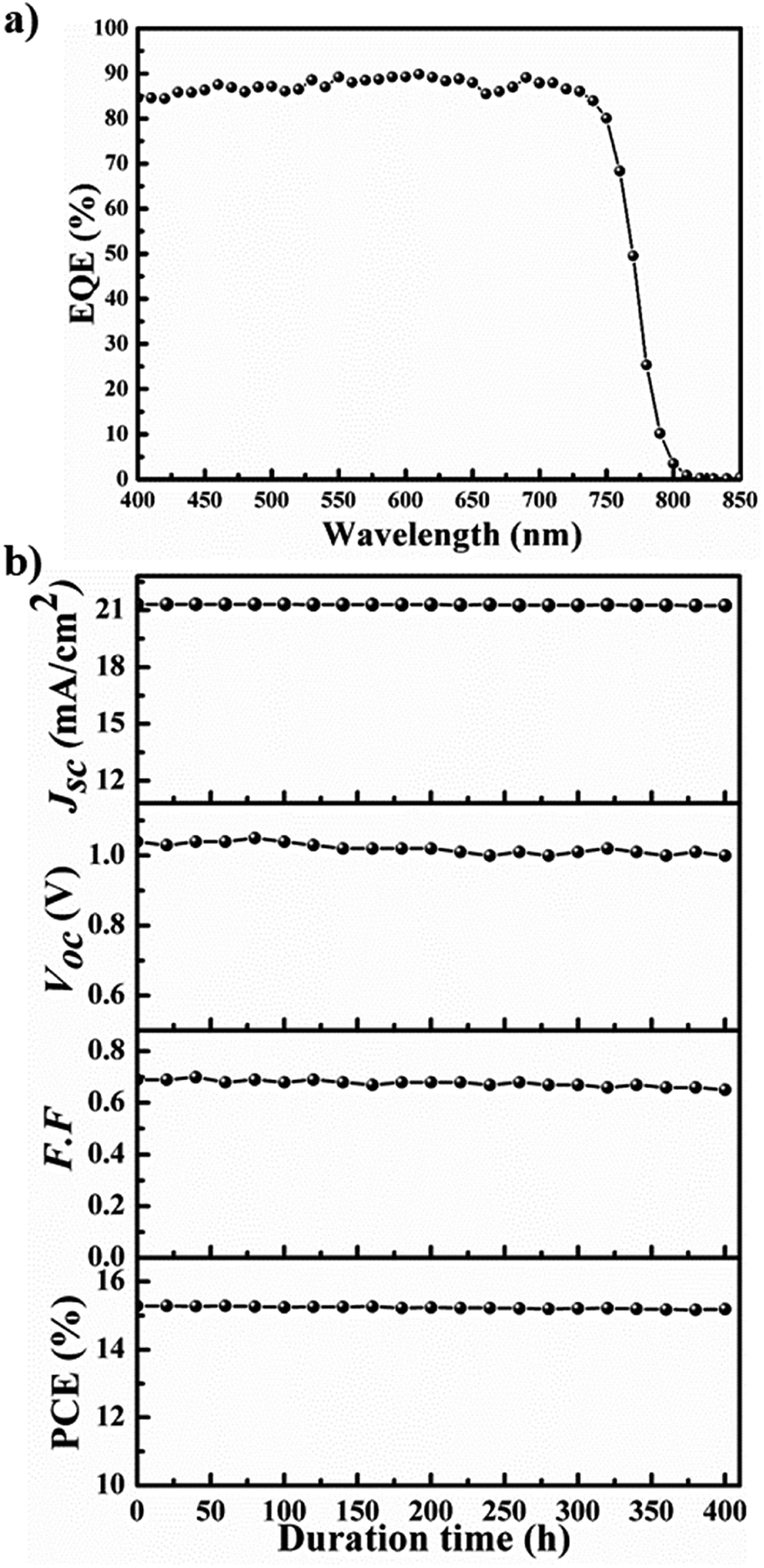 | ||
| Fig. 6 (a) EQE spectra and (b) stability for the most efficient PrSC devices with the MAPbI3−xClx perovskite layer prepared in 0.75-MACl/MAI. | ||
4. Conclusion
We have demonstrated the preparation of highly efficient MAPbI3−xClx perovskite materials using a simple, sequential all-dip-coating deposition in an aqueous non-halide lead precursor solution and MACl/MAI mixed solution toward a facile, cost-effective, and environmentally benign manufacturing processes for high-efficiency PrSCs. The MAPbI3−xClx perovskite layers deposited via this dip-coating process were constructed with a Cl/I ratio below ∼3%, indicating the partial insertion of Cl into the MAPbI3 perovskite lattice. The inserted amounts of Cl were readily modulated by varying the MACl concentration in the MAI and MACl mixed solution. A slight Cl incorporation led to significant improvements in the surface morphology and crystallinity of the MAPbI3−xClx perovskite layer compared to those of MAPbI3 fabricated under the same conditions. PrSC devices fabricated with these perovskite films exhibited superior device performances and stabilities, resulting in an outstanding PCE of ∼15.3%. Thus, we successfully realized highly efficient MAPbI3−xClx perovskite materials with an aqueous non-halide lead precursor, in contrast to the conventional spin-casting approach that requires toxic organic solvents and have substrate size restrictions. The results of this study lay the groundwork for environmentally benign and low-cost manufacture of high-efficiency PrSCs.Conflicts of interest
The authors declare no conflict of interest.Acknowledgements
This work was financially supported by Basic Science Research Program through the National Research Foundation of Korea (NRF-2018R1A2B6003669).References
- R. P. Xu, Q. Y. Li, Y. T. Jin, Q. Y. Liu, Y. Q. Bao, C. Carroll and X. J. Tang, In Situ Observation of Light Illumination-Induced Degradation in Organometal Mixed-Halide Perovskite Films, ACS Appl. Mater. Interfaces, 2018, 10(7), 6746 Search PubMed.
- M. Saliba, T. Matsui, J. Y. Seo, K. Domanski, J. P. Correa-Baena, M. K. Nazeeruddin, S. M. Zakeeruddin, W. Tress, A. Abate, A. Hagfeldt and M. Grätzel, Cesium-Containing Triple Cation Perovskite Solar Cells: Improved Stability, Reproducibility and High Efficiency, Energy Environ. Sci., 2016, 9(6), 1997 RSC.
- N. J. Jeon, H. Na, E. H. Jung, T. Y. Yang, Y. G. Lee, G. Kim, H. W. Shin, S. I. Seok, J. Lee and J. Seo, A Fluorene-Terminated Hole-Transporting Material for Highly Efficient and Stable Perovskite Solar Cells, Nat. Energy, 2018, 3(8), 689 Search PubMed.
- H. J. Heo, H. M. Lee, H. M. Jang and H. S. Im, Highly Efficient CH3NH3PbI3−xClx Mixed Halide Perovskite Solar Cells Prepared by Re-Dissolution and Crystal Grain Growth via Spray Coating, J. Mater. Chem. A, 2016, 4(45), 17642 RSC.
- F. J. Wang, L. Zhu, G. B. Zhao, L. Y. Zhao, J. Song, Q. X. Gu and H. Y. Qiang, Surface Engineering of Perovskite Films for Efficient Solar Cells, Sci. Rep., 2017, 7(1), 9 CrossRef PubMed.
- M. Jiang, J. Wu, F. Lan, Q. Tao, D. Gao and G. Li, Enhancing the Performance of Planar Organo-Lead Halide Perovskite Solar Cells by Using a Mixed Halide Source, J. Mater. Chem. A, 2015, 3(3), 967 RSC.
- N. J. Jeon, J. H. Noh, Y. C. Kim, W. S. Yang, S. Ryu and S. I. Seok, Solvent engineering for high-performance inorganic-organic hybrid perovskite solar cells, Nat. Mater., 2014, 13(9), 897 CrossRef CAS PubMed.
- H. Tan, A. Jain, O. Voznyy, X. Lan, G. P. F. De Arquer, Z. J. Fan, R. Quintero Bermudez, M. Yuan, B. Zhang, Y. Zhao, F. Fan, P. Li, N. L. Quan, Y. Zaho, H. Z. Lu and Z. Yang, Efficient and Stable Solution-Processed Planar Perovskite Solar Cells via Contact Passivation, Science, 2017, 355(6326), 722 CrossRef CAS PubMed.
- M. Adnan and J. K. Lee, All Sequential Dip-Coating Processed Perovskite Layers from an Aqueous Lead Precursor for High Efficiency Perovskite Solar Cells, Sci. Rep., 2018, 1, 2168 CrossRef PubMed.
- M. Adnan and J. K. Lee, Highly Efficient Planar Heterojunction Perovskite Solar Cells with Sequentially Dip-Coated Deposited Perovskite Layers from a Non-Halide Aqueous Lead Precursor, RSC Adv., 2020, 10(9), 5454 RSC.
- Q. Dong, Y. Yuan, Y. Shao, Y. Fang, Q. Wang and J. Huang, Abnormal Crystal Growth in CH3NH3PbI3-XClx Using a Multi-Cycle Solution Coating Process, Energy Environ. Sci., 2015, 8(8), 2464 RSC.
- S. Colella, E. Mosconi, P. Fedeli, A. LIstorti, A. Rizzo, F. Gazza, F. Orlandi, P. Ferro, T. Besangi, G. Calentani, F. DeAngelis, R. Mosca and G. Gilgi, MAPbI3-XClx Mixed Halide Perovskite for Hybrid Solar Cells: The Role of Chloride as Dopant on the Transport and Structural Properties, Mater. Res. Soc. Symp. Proc., 2014, 1667 Search PubMed.
- R. M. Ahmadin-Yazdi, F. Zabihi, M. Habibi and M. Eslamian, Effects of Process Parameters on the Characteristics of Mixed-Halide Perovskite Solar Cells Fabricated by One-Step and Two-Step Sequential Coating, Nanoscale Res. Lett., 2016, 11(1), 408 CrossRef PubMed.
- S. Maniarasu, K. M. Rajbhar, K. r. Dileep, E. Ramasamy and G. Veerappan, Hole-Conductor Free Ambient Processed Mixed Halide Perovskite Solar Cells, Mater. Lett., 2019, 245, 226 CrossRef CAS.
- T. Hwang, D. Cho, J. Kim, J. Kim, S. Lee, B. Lee, H. K. Kim, S. Hong, C. Kim and B. Park, Investigation of Chlorine-Mediated Microstructural Evolution of CH3NH3PbI3(Cl) Grains for High Optoelectronic Responses, Nano Energy, 2016, 25, 91 CrossRef CAS.
- B. Lee, T. Hwang, S. Lee, B. Shin and B. Park, Microstructural Evolution of Hybrid Perovskites Promoted by Chlorine and Its Impact on the Performance of Solar Cell, Sci. Rep., 2019, 9(1), 4803 CrossRef PubMed.
- T. Y. Hsieh, M. Pylnev, E. Palomares and T. C. Wei, Exceptional long electron lifetime in methylammonium lead iodide perovskite solar cell made from aqueous lead nitrate precursor, Adv. Funct. Mater., 2020, 30(10), 1909644 CrossRef CAS.
- T. Y. Hsieh, T. C. Wei, K. L. Wu, M. Ikegami and T. Miyasaka, Efficient perovskite solar cells fabricated using an aqueous lead nitrate precursor, Chem. Commun., 2015, 51, 13294 RSC.
- D. V. Shinde, L. Pyeon, M. Pei, G. W. Kim, H. Yang and T. Park, Enhanced efficiency and stability of an aqueous lead nitrate based organometallic perovskite solar cell, ACS Appl. Mater. Interfaces, 2017, 9(16), 14023 CrossRef CAS PubMed.
- Y. Sun, H. J. Seo, J. C. Takacs, J. Seifter and J. A. Heeger, Inverted Polymer Solar Cells Integrated with a Low-Temperature-Annealed Sol-Gel-Derived ZnO Film as an Electron Transport Layer, Adv. Mater., 2011, 23(14), 1679 CrossRef CAS PubMed.
- B. Philoppe, W. B. Park, R. Lindblad, J. Oscarsson, S. Ahmadi, J. M. E. Johansson and H. Rensmo, Chemical and Electronic Structure Characterization of Lead Halide Perovskites and Stability Behavior under Different Exposures-A Photoelectron Spectroscopy Investigation, Chem. Mater., 2015, 27(5), 1720 CrossRef.
- Y. Zhao and K. Zhu, CH3NH3Cl-Assisted One-Step Solution Growth of CH 3NH3PbI3: Structure, Charge-Carrier Dynamics, and Photovoltaic Properties of Perovskite Solar Cells, J. Phys. Chem. C, 2014, 118(18), 9412 CrossRef CAS.
- L. E. Unger, R. A. Bowring, J. C. Tassone, L. V. Pool, A. Gold-Parker, R. Cheacharoen, K. H. Stone, E. T. Hoke, M. F. Toney and M. D. McGehee, Chloride in Lead Chloride-Derived Organo-Metal Halides for Perovskite-Absorber Solar Cells, Chem. Mater., 2014, 26(24), 7158 CrossRef.
- S. Colella, E. Mosconi, P. Fedeli, A. Listorti, F. Gazza, F. Orlandi, P. Ferro, T. Besagni, A. Rizzo, G. Calestani, G. Gigli, F. D. Angelis and R. Mosca, MAPbI3−XClX mixed halide perovskite for hybrid solar cells: The role of chloride as dopant on the transport and structural properties, Chem. Mater., 2013, 25(22), 4316 CrossRef.
- O. Malinkiewicz, A. Yella, H. Y. Lee, M. G. Espallargas, M. Graetzel, K. M. Nazeeruddin and J. H. Bolink, Perovskite Solar Cells Employing Organic Charge-Transport Layers, Nat. Photonics, 2014, 8(2), 128 CrossRef CAS.
- L. E. Unger, T. E. Hoke, D. C. Bailie, H. Y. Nguyen, R. A. Bowring, T. Heumuller, G. M. Christoforo and D. M. McGehee, Hysteresis and Transient Behavior in Current-Voltage Measurements of Hybrid-Perovskite Absorber Solar Cells, Energy Environ. Sci., 2014, 7(11), 3690 RSC.
Footnote |
| † Electronic supplementary information (ESI) available. See DOI: 10.1039/d0ra06074g |
| This journal is © The Royal Society of Chemistry 2020 |